Taylor Schweizer
-
Day... something. Controller Board!
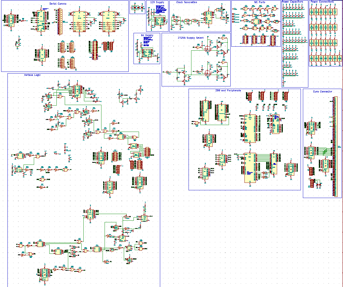
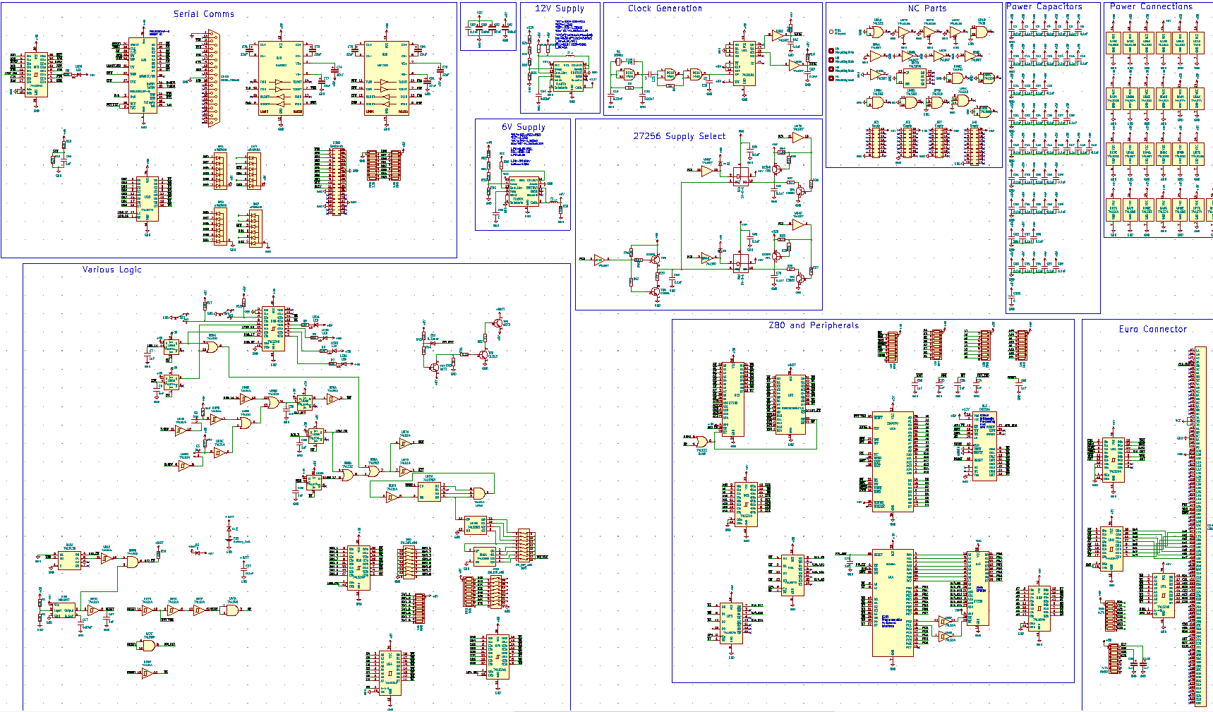
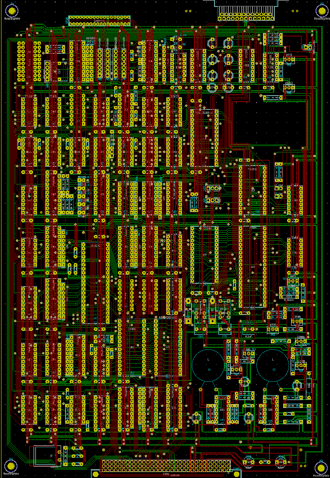
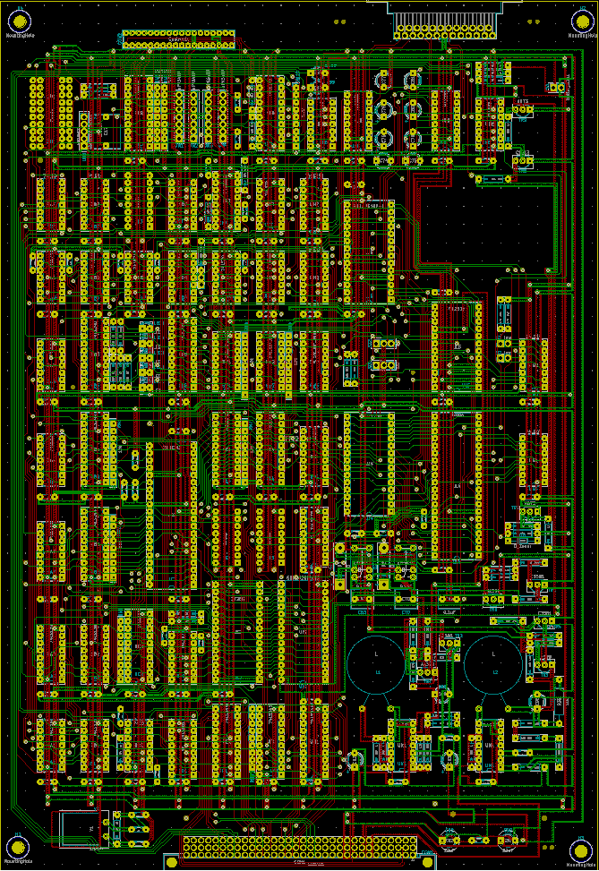
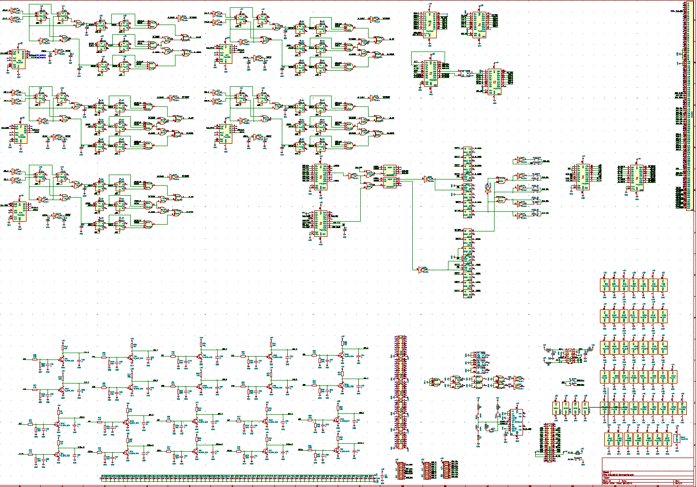
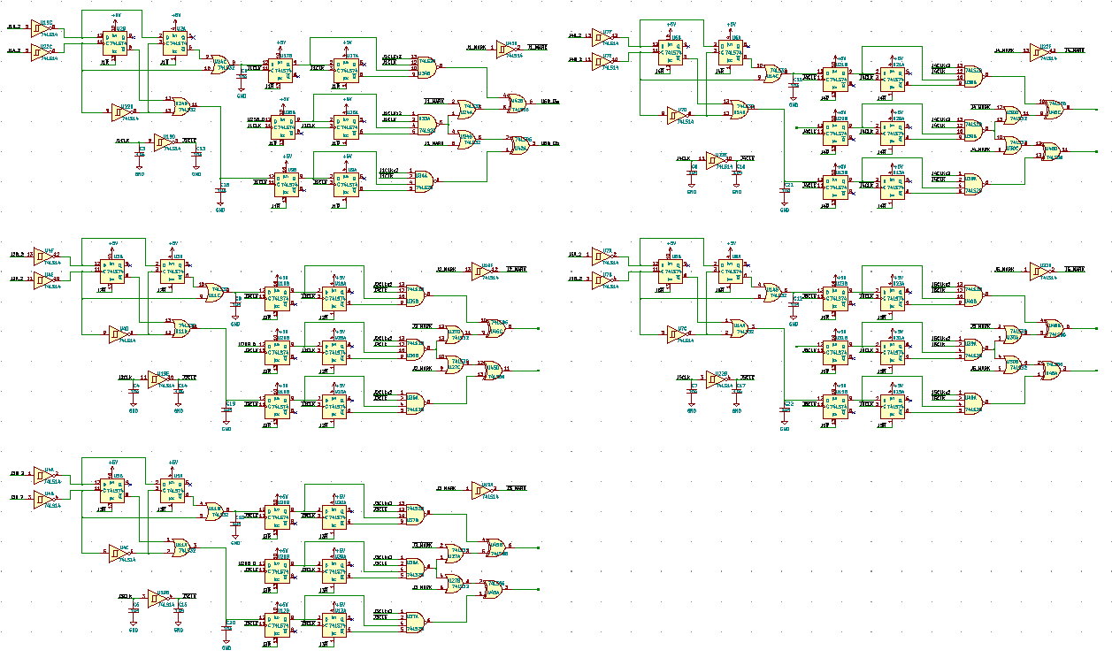
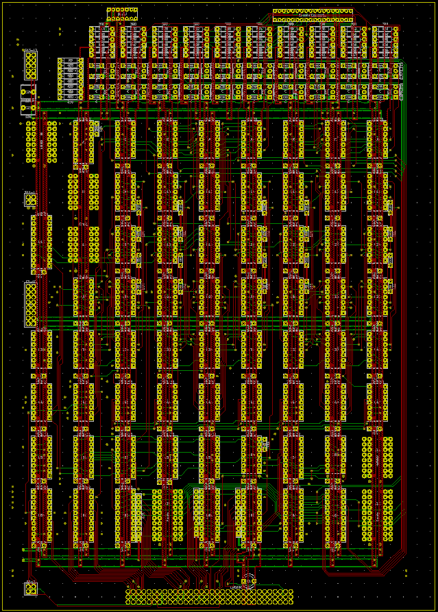
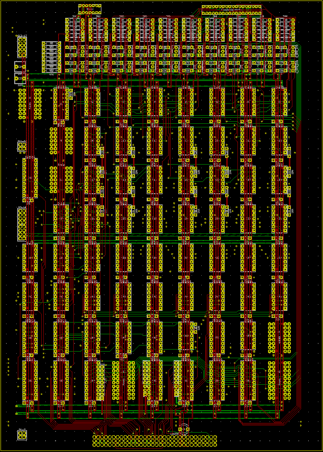
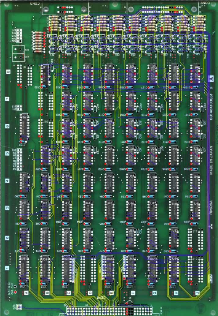
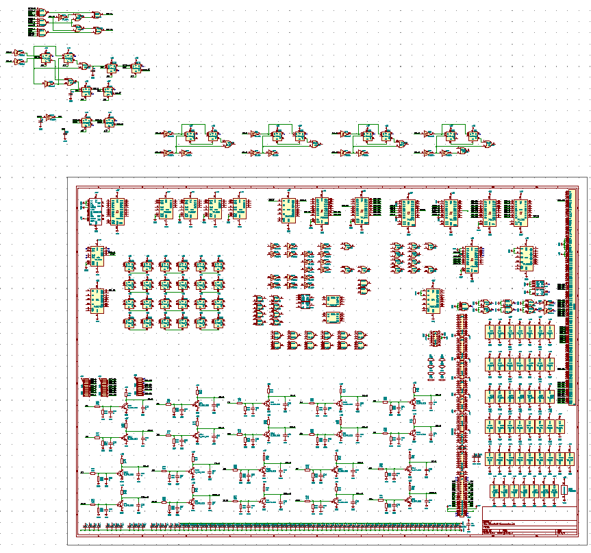
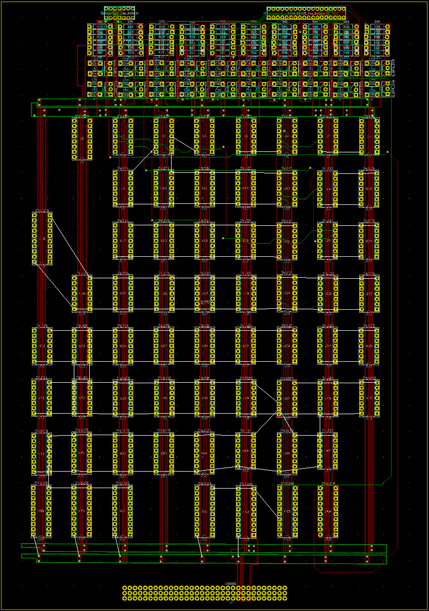
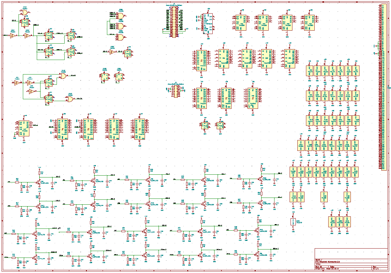
01/10/2021 at 04:25 • 0 commentsSo I finally got some time to continue working on this. I've been reversing the main controller board with the Z80 Processor. I'll do a better write up once I get all of the digital logic sorted out, but this is what I've got so far. I've got all of the connections made on the board, the only thing that's left is to layout the schematic better so it makes sense. Basically my methodology for reversing these boards tends to use a lot of nets and parts are just scattered all over since I don't know the design intent, and I have to go through each sub-circuit, determine the design intent and functionality, then lay the sub-circuit out in a more appealing way. You can see an example of this in one of the original schematics I had for the motor signal condition board, and the final layout (original, final).
![]()
![]()
![]()
![]()
-
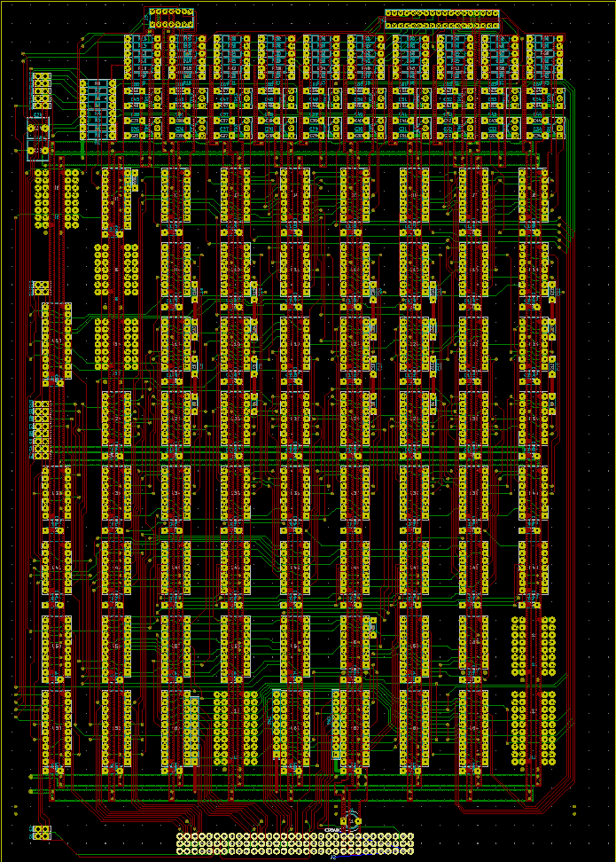
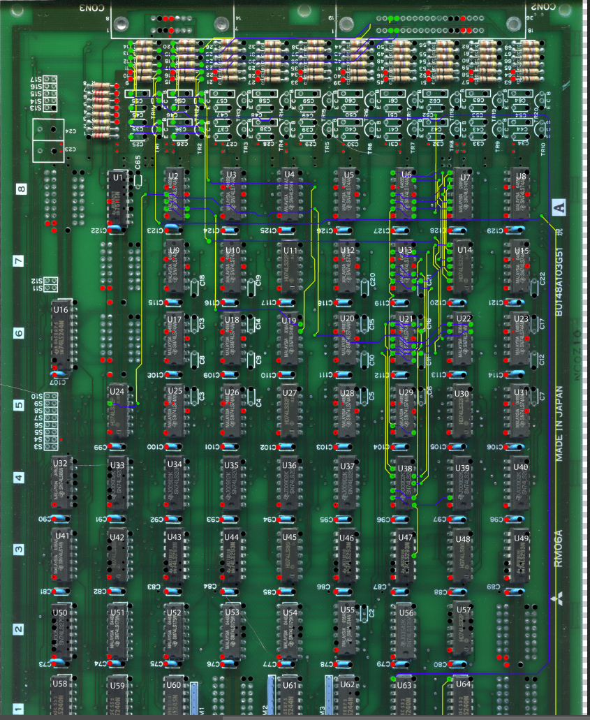
Reverse Engineering Motor Signal Board Day 9 - Done!
06/11/2020 at 17:39 • 1 commentOr as done as I'll ever be. I've got all the traces finished and the layout complete. Some things still don't make too much sense, but I won't be able to figure them out until I finish the main processor board and figure out what those connections are doing.
Next up I think I want to make a DIN 41612 extension cable so I can do some probing on the board while it is running, followed by making a smaller version of the board.
Just for fun, I thought I'd see how much this board would cost on Oshpark - $476! These boards are huge.
![]()
![]()
-
Reverse Engineering Motor Signal Board Day 8 - Finally figured out the clock!
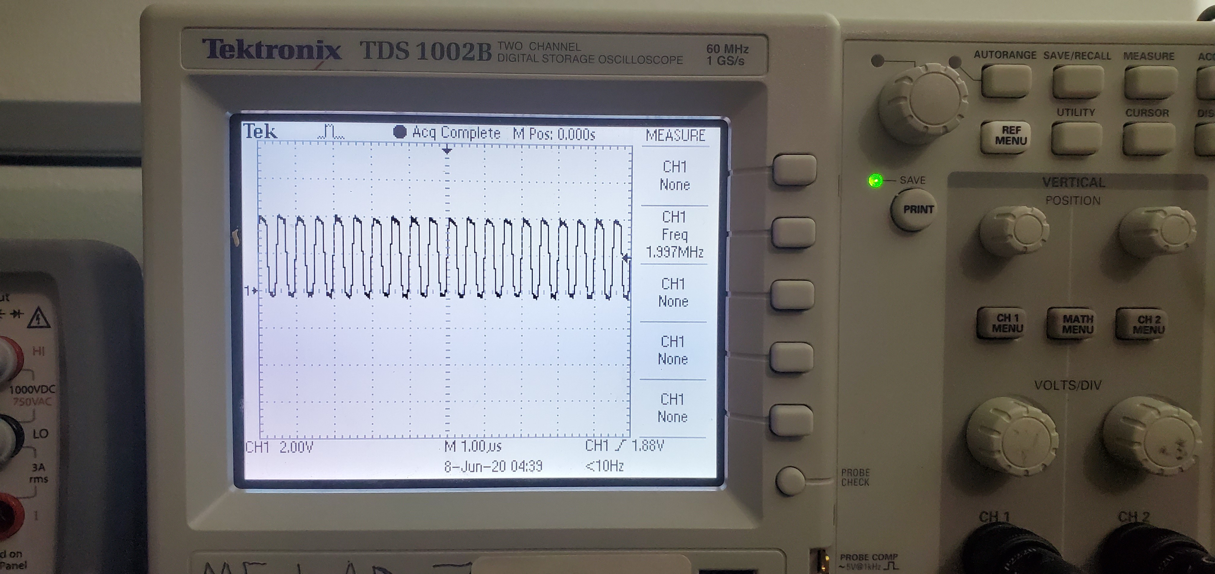
06/08/2020 at 02:20 • 0 commentsI finally figured out the clock that is running to all of the flip flops! There is a 2MHz clock signal coming from the main CPU board that goes into a 4 bit counter, and the flip flop clock is using the uppermost bit so it is effectively divided by 8. There is also a signal coming from the second bit, so it is the clock divided by 4, going into the 4 input NAND gate. What that means is the flip flops are clocked on a 250 kHz signal.
I also finished tracing all of the encoder logic channels. All that remains is the final bits of logic involving multiplexers and stuff.
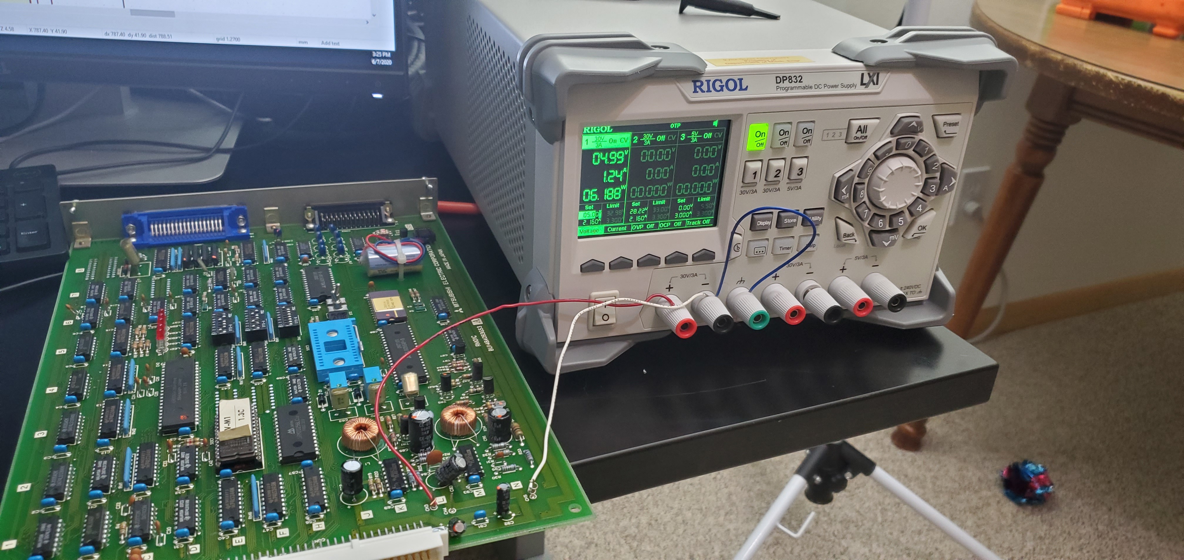
Powering the main CPU board:
![]()
![]()
And the schematic/PCB
![]()
![]()
-
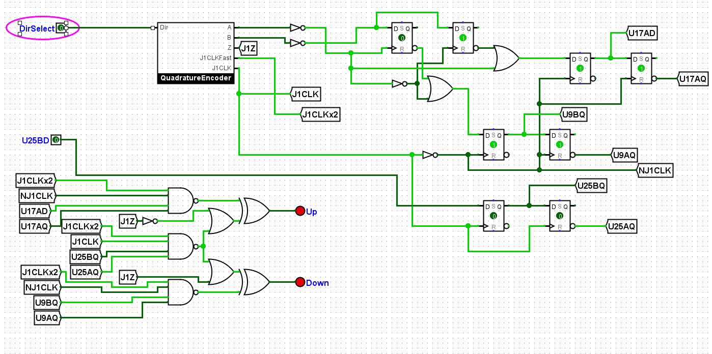
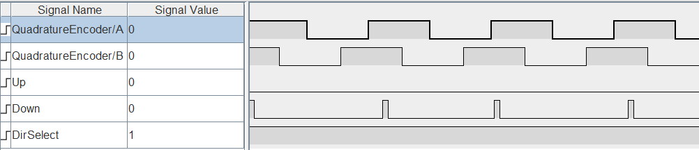
Reverse Engineering Motor Signal Board Day 7 - Simulated Circuit, still confused
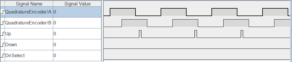
06/07/2020 at 00:15 • 0 commentsSo I went ahead and simulated what I had so far for the joint 1 encoder circuit using Logisim Evolution. It looks like a simple converter between the quadrature output of the encoder to an up/down signal, and it uses the index signal and the limit switch as a reset. Take a look (ignore the clocks and stuff, I haven't quite figured out how they are connected - also the DirSelect on the left side of the screen is what I use to change the direction of the encoder i.e. whether A or B is leading or lagging):
![]()
Here's the chronogram:
![]()
![]()
I'm still tracing back the stuff involving the Z index marker on the encoder, as well as the limit switch.
Here's the KiCAD PCB so far:
![]()
-
Reverse Engineering Motor Signal Board Day 6 - Weird ground shield, new ideas
06/05/2020 at 03:05 • 0 commentsThis is getting extremely complicated extremely fast. A few things I've noticed (is anyone even reading these logs?):
- It seems as though the encoder channels have an auto zero function, as well as possibly an error correction? Either error correction or some type of position-to-speed calculation.
- There is a clock signal coming from the main board, and all of the traces are surrounded with a weird ground shielding trace. I'll post a picture below.
- I had to pull out the board that all of these large boards plug into to trace where the clock signal is coming from. Looks like they are using a binary counter to divide clock signals.
Here's my idea - I really, really want to make an identical board but with modern components. For instance, instead of using the 20 pin DIP packages for the SN74LS240N, I want to use the 20 pin SOIC package. Replace all transistors with a sot-23 package, resistors with 0805 SMD, etc. Basically I want a board with the exact same number of items on the BOM, but with all SMD parts. Just to see how small I can make the board. No idea if I'll actually do this or not, really seems like I'm writing this just for myself.
There will be a few pictures today, the usual zoomed out view as well as some specifics on both the layout and the schematic.
![]()
![]()
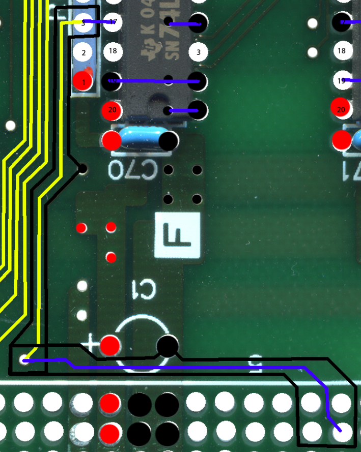
Here is the weird ground trace. Quick color convention - blue traces are on the bottom, yellow traces are on top, the black traces are ground traces. They surround the clock trace.
![]()
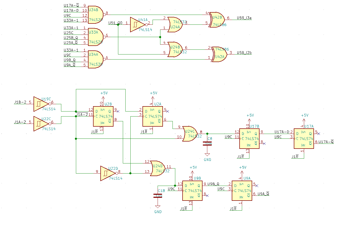
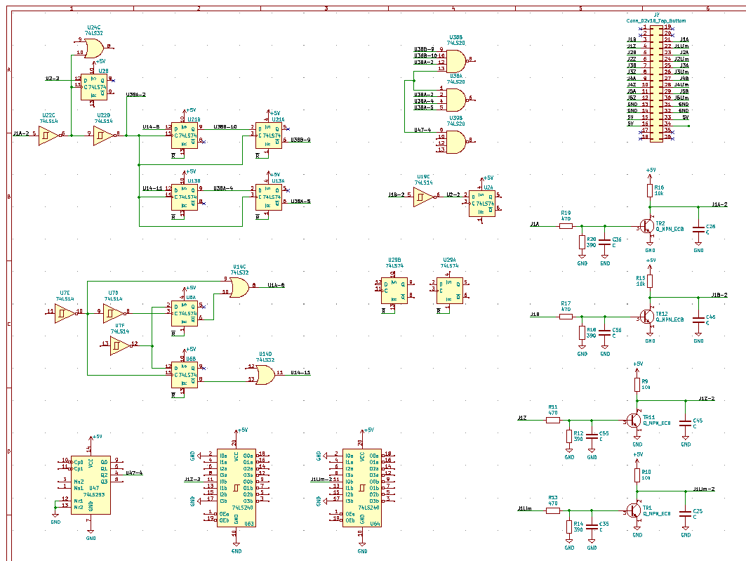
Here is most of the schematic for the encoder for joint 1. This is just one joint. There are 4 more. But just like the input conditioning, it seems to be duplicated.
![]()
-
Reverse Engineering Motor Signal Board Day 5 - Restart, ugh
06/03/2020 at 21:22 • 0 commentsSo I realized something - the entire board is laid out on a 0.100" grid. Every single pin of every part (besides two connectors that have a 0.085" pitch) is on that grid. And it lines up. Knowing this, I went back to photoshop and used this to make sure the board was square and exported a second hole layout, and re-layed out the entire board in KiCad. I also found that all of the vias were on a 0.050" grid, and the tracks on a 0.025" grid. This makes laying out much, much easier.
The reason I redid this was because there is a bit of a difficulty with the way I do reverse engineering - basically if the scan of the PCB doesn't result in a perfectly square image, there is usually a slant to the traces and pin layouts. To counteract that, I usually use a very small grid when running traces so I can run traces and stuff to accommodate the misalignment. But since everything is on the grid I mentioned before, I could make sure everything was aligned properly.
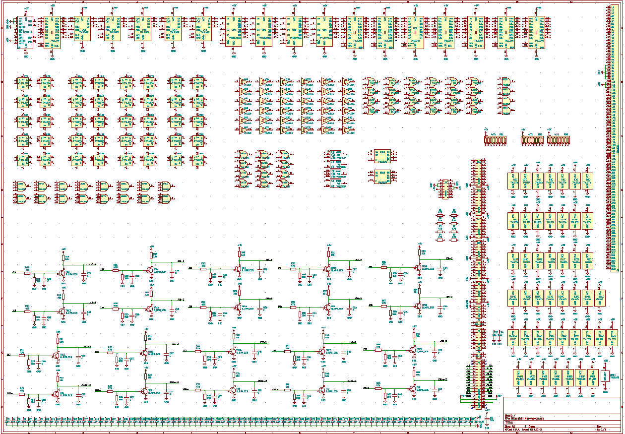
I also went ahead and added all of the power capacitors and various connectors and stuff. I'm already using an A2 size page for the layout, and I just about have it filled with the empty components. This is getting wildly out of control.
![]()
![]()
-
Reverse Engineering Motor Signal Board Day 4 - Full Board
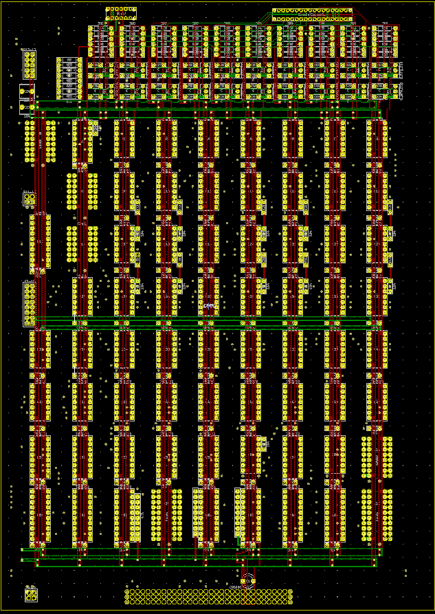
06/02/2020 at 00:38 • 0 commentsI decided to just reverse the entire board. Less error prone that way. I've got all the IC footprints on the board, most of the resistors and capacitors, and most of the filled zones.
![]()
![]()
This is testing my patience.
-
Reverse Engineering Motor Signal Board Day 3 - More PCB Tracing, getting weird
05/31/2020 at 20:52 • 0 commentsMore plugging and chugging with reversing the PCB, I think I'm going to have to just do a full reverse engineer. So many of the digital traces are tied into each other that without doing them all it doesn't seem to be making much sense.
![]()
![]()
-
Firmware Dump
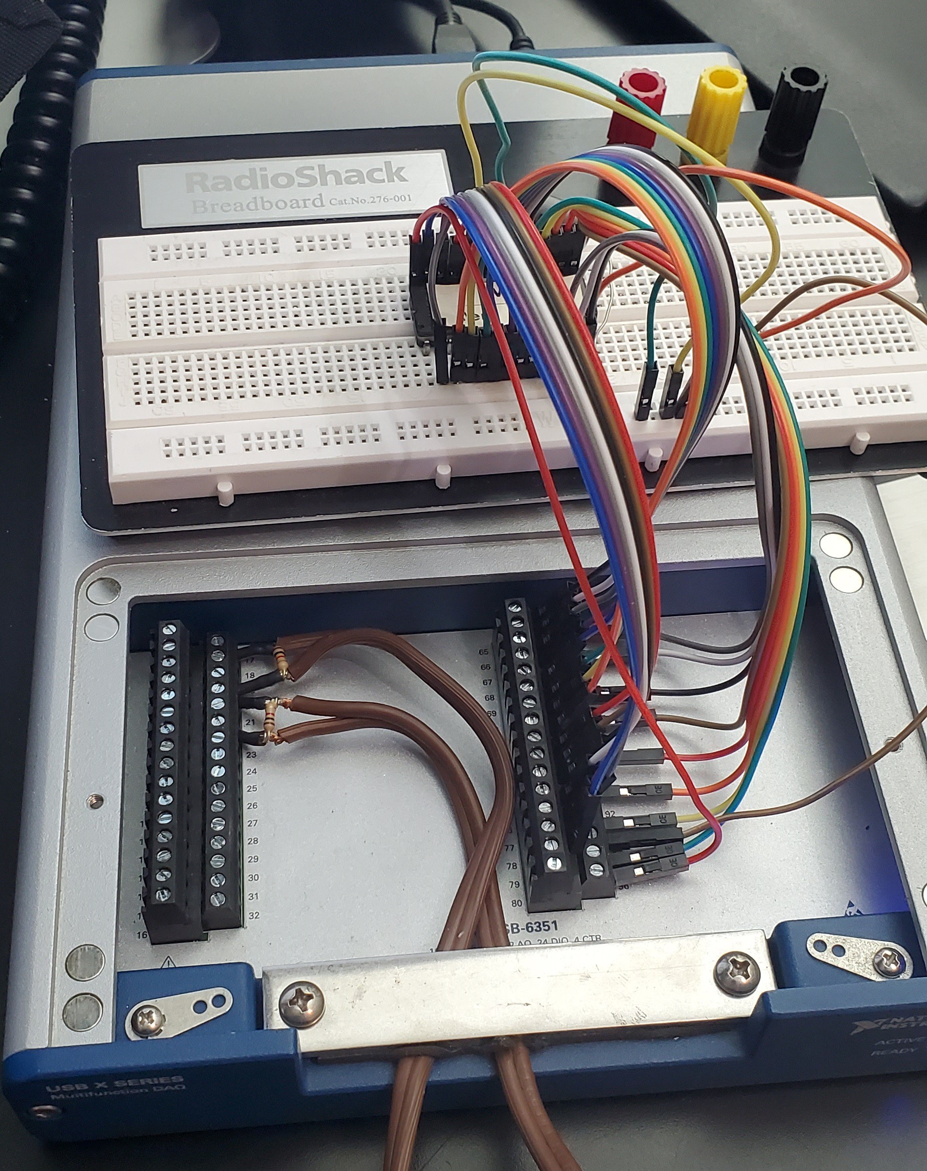
05/26/2020 at 22:24 • 1 commentThe firmware for the arm is on an old D27256 EPROM, and the processor is a LG0080A running the Z80A instruction set. Getting a dump of the firmware is easy enough with an Arduino or something, unfortunately I only have some Teensies that aren't 5V compatible so I had to use some industrial equipment.
Introducing the National Instruments USB-6351.
![]()
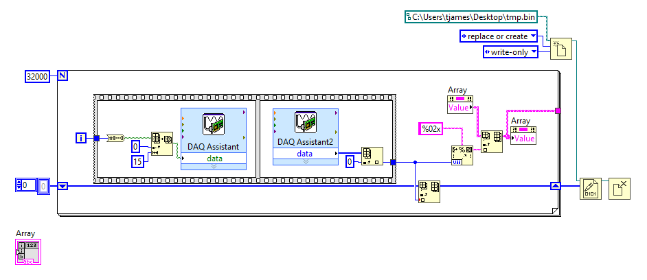
Using a simple Labview program I pulled the data off the chip and into a binary file.
![]()
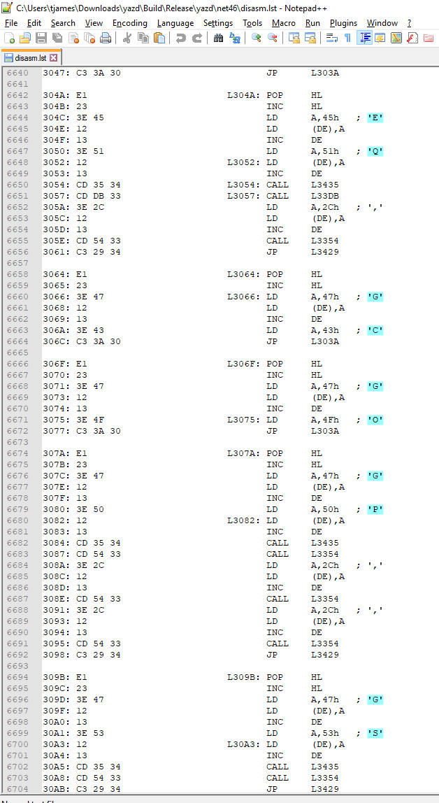
I then found this Z80 Disassembler and took a peak at the file. I found some ASCII characters being loaded into the register, and they correspond to some of the programming commands. This made me confident that I at least got the connections and stuff right.
From the disassembler:
![]()
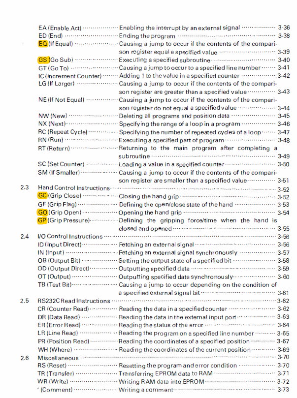
And from the robot manual:
![]()
-
Reverse Engineering Motor Signal Board Day 2
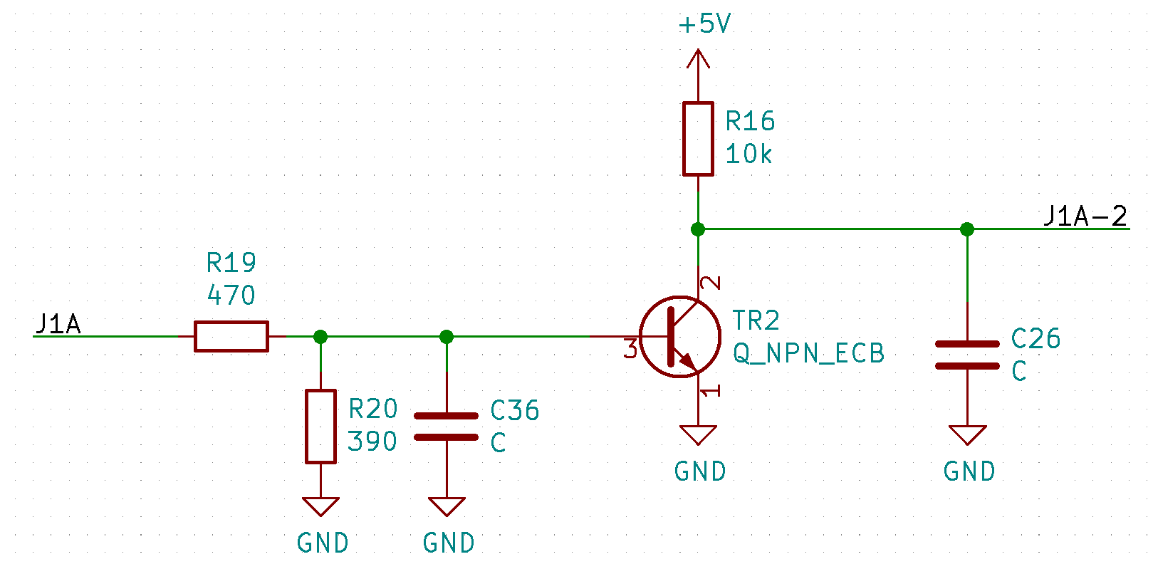
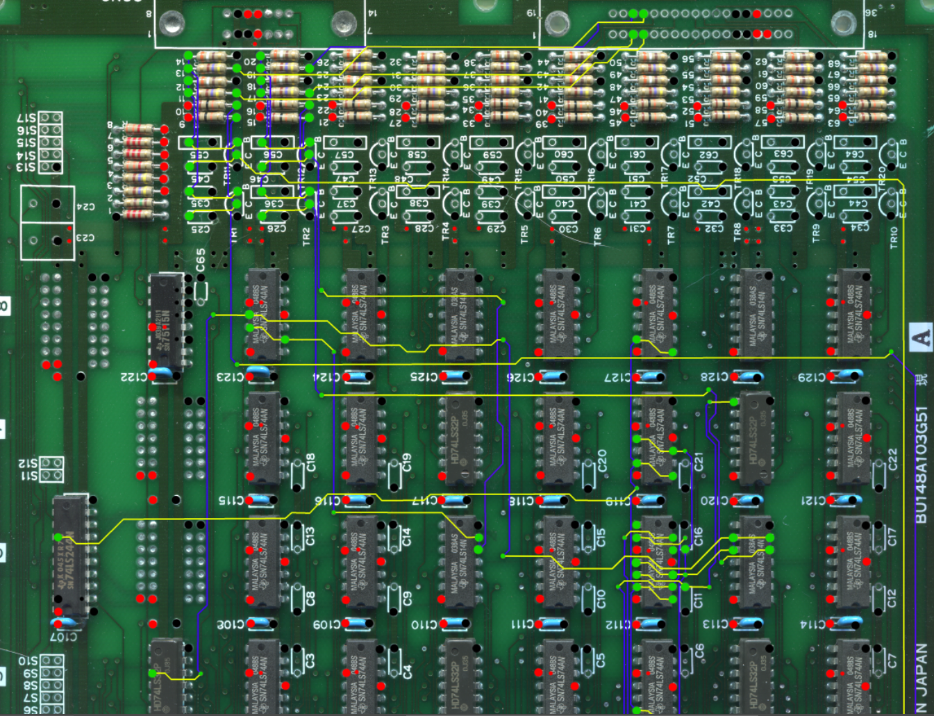
05/16/2020 at 21:17 • 0 commentsI'm going through and following the encoder pins for Channel 1. So far I've found that the encoder channels go into a basic transistor switch circuit:
![]()
Then it goes into the 74 series logic. This is taking a long time to trace, but here's my progress so far (I have a few more components with various nets off to the side).
![]()
Photoshop progress
![]()
Reviving and Reverse Engineering an Old Robot Arm
A full reverse engineering and rebuild of a Mitsubishi Movemaster robotic arm