PMercier
-
Happy ending
05/13/2022 at 20:38 • 1 commentSince the last post a prototype was created with WiFi, Ethernet and an extension slot. As many prototype when you are green behind the ears, it had problems. I learned a lot with it during the hardware debugging. It took nearly one week to solve it (it was a chair/keyboard interface problem ;) ).
But life and work can be really unpredictable. I had a LOAD OF WORK due to people leaving the company to have a better job/salary. I was the last of the teams and as i am lead/manager i was tasked to build an entire teams. Covid pandemic wasn't a big time to find good developers or project/product managers. You can easily see where it going. I had to be a Cloud Developer, a Data Engineer, an Application Architect, an Admin Sys, a Product Owner and a Project Manager, but i suxx in the last two and was a junior in the first two.
I had to make a choice. My work was an hell as i had to do every thing to complete the project i initiated one year ago. But man, it was a hellish fun time as it revolved around many tech i never worked with and wanted to play with (dev syndrom). You can guess i choose my work over my electronic hobbies, the first one paying what my family eat.I now have the time to continue this project as i achieved to solve my problems by finding competent peoples to replace me in what am really bad at and to help me at completing/maintaining the project (including some IA).
BUT, now that i have time for my hobbies, I saw this project becoming obsolete :)
Someone used my work to complete/start a new version of his own, correcting some of my errors. It's what i love love on the net, share something and see it grow behind what you sawn. I'am not saying that i initiated this move toward his project, am just glad that what i did was usefull to even one person and that i was able to contribute somehow.
I took a look at what he did a saw he even gone behind what i intended to do on my first prototype. I wanted to add an Ethernet using an ESP, but he did it by using the native TDS3K Ethernet capabilities plus WiFi. More than that he included a way to solve the common problem of old TDS3K scopes : dead NVRAM.
Even if what he did won't answer all of my needs/wishes, it solve a lot of them. As such I won't probably work anymore on this project and adopt his.
That's why I'll had here the links to his work :
* https://www.eevblog.com/forum/testgear/reverse-engineering-tektronix-tds3gv-module-for-tds3000-series-oscilloscopes/msg3427926/#msg3427926* https://www.eevblog.com/forum/testgear/tds3000c-series-bw-sampling-hack/msg3427884/#msg3427884
It wouldn't be fair to mention and thank only Sicco (the board creator) so i'll say it another way :
Thank you the great eevblog community, and all of the people that contributed in making my TDS3K scopes more usable !!!!
-
The actual informations
06/19/2020 at 21:16 • 1 commentDetecting and identifying a card
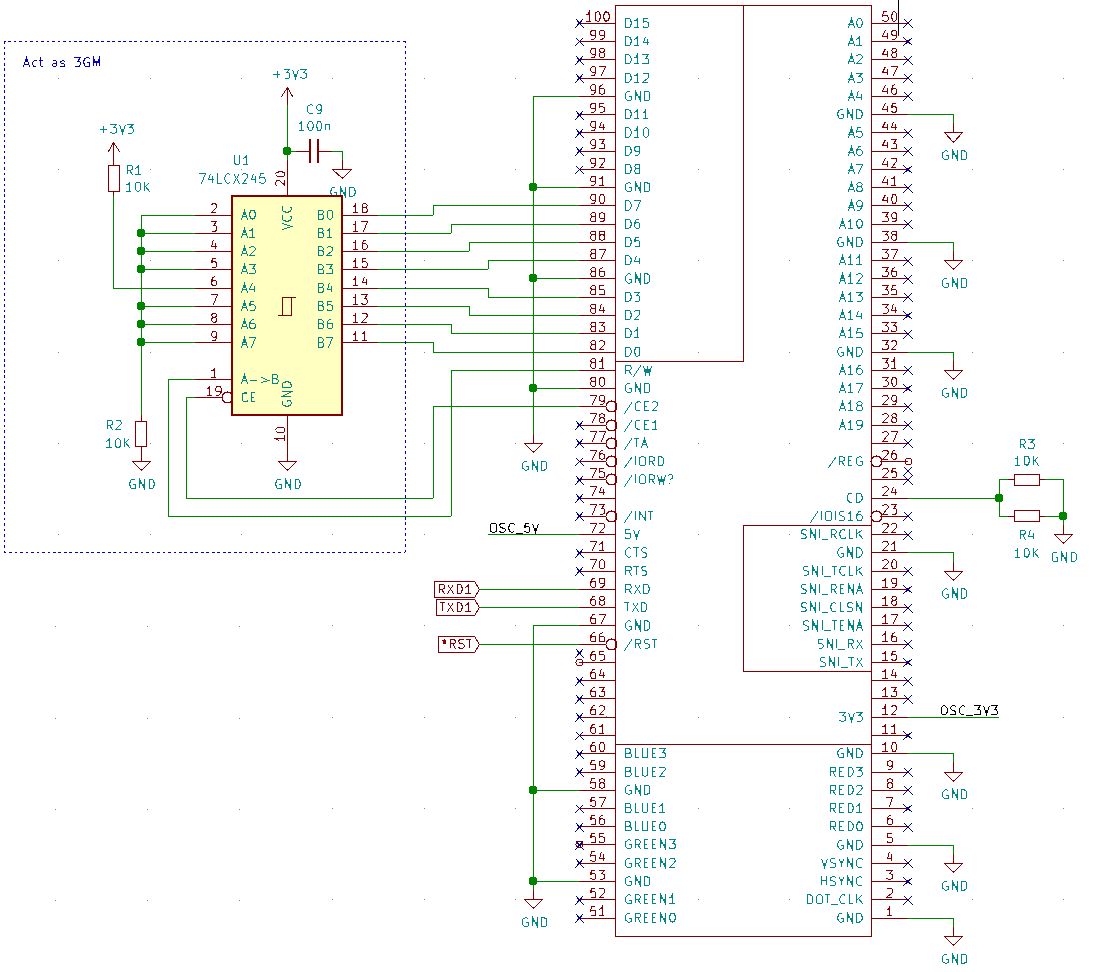
As stated in an earlier log, the card insertion is detected by grounding the pin *CD. But this is not enough to make the scope believe he have a know card inside him. You need to indicate him what type of card was inserted.
This is done by writing a byte on the data bus when the *CE2 and R/W signals are low.
The extensions card have a simple way to do it, they use a single LCX245 as a single byte ROM.
From what I could see on all the photos of the different modules, it was easy to guess that one card type was one bit set to 1 and 0 for the others.
     | 7654 3210 | Scope
-----+-----------+-------------------------------------------------
0x00 | 0000 0000 | Scope ask a new firmware
0x01 | 0000 0001 | Scope ask a new firmware
0x02 | 0000 0010 | TDS3GV is detected
0x04 | 0000 0100 | The scope won't boot past the logo
0x08 | 0000 1000 | TDS3GM is detected
0x10 | 0001 0000 | 3VM is detected
0x20 | 0010 0000 | 3VM is detected
0x30 | 0100 0000 | 3VM is detected
0x40 | 1000 0000 | 3VM is detected
For the 0x00, and 0x01 bytes they seem to be reserved for special cards who need firmware update to add some option inside the scope.
And the 0x04 byte, we can assume that's the TDS3EV with the Ethernet port. As the scope can't read the flash present on the card, he don't know what to do so he's waiting. I though it could be that he's trying to contact the Ethernet chip, but it's unlikely as the MC68160 is just a dumb transceiver using an SNI interface.
79  *CE2
81  R/W
The SNI/SIA interface
The main CPU, the MPC860 inside the TDS3K serie come with an integrated Ethernet controller.
By following the exposed tracks on the 3EV card photos the pins positions were found and the missing ones were deduced using the proximity of the tracks with each other. These SNI lines are present on the extension port of the "A" model.
But on the C model, the SNI lines are sent to an LXT905 (Eth transceiver) near the power supply and are not presents on the extension port. As the B model as the same type of native Ethernet port you can expect these lines to be missing too.
I still have to test a possibility on the A model to see if the TCP/IP stack is present, but I'll need an SNI chip for that. I already checked the lines on the A model, but nothing append. So perhaps the scope won't activate the stack until he get a receive clock from the SNI lines.
15  TD     Tranmit Data
16  RD     Receive Data
17  TENA   Transmit ENAbled input
18  CLSN   CoLiSioN
19  RENA   Receiver ENAbled output
20  TCLK   Transmit CLocK input
22  RCLK   Receive CLocK output
The screen output
With or without an extension card, the screen signals are always presents on the port as they are connected to the LCD connector with some discrete and passive components.
The 640x480 screen is refreshed at 60Hz.
Be aware : I'am confident that red pins are red, green ones are green and blue are blues. But the position of the color bits can be wrong. I used the scope himself and played with the screen colors to find them.
And yes, only 4 bits per colors are presents on the extension port, like the LCD connector.
2   DotClock  25MHz square signal
3   HSync     31.5KHz, 88% duty cycle, 31.72µs high and 3.82µs low
4   VSync     60Hz, 99.6% duty cycle
5   GND
6   Red[0]
7   Red[1]
8   Red[2]
9   Red[3]
10  GND
51  Green[0]
52  Green[1]
53  GND
54  Green[2]
55  Green[3]
56  Blue[0]
57  Blue[1]
58  GND
59  Blue[2]
60  Blue[3]
Address and data lines
After probing the CPU, the memory chips and more "photoshopping" here are the data lines :
82   D0           28  A19
83   D1           29  A18
84   D2           30  A17
85   D3           31  A16
86   GND          32  GND
87   D4           33  A15
88   D5           34  A14
89   D6           35  A13
90   D7           36  A12
91   GND          37  A11
92   D8           38  GND
93   D9           39  A10
94   D10          40  A9
95   D11          41  A8
96   GND          42  A7
97   D12          43  A6
98   D13          44  A5
99   D14          45  GND
100  D15          46  A4
                  47  A3
                  48  A2
                  49  A1
                  50  A0
The serial port lines
The serial port lines was provided by james_s from the EEVBlog forum.
68  TXD
69  RXD
70  RTS
71  CTS
When discussing on the forum and doing some test case, it seem the serial port is always active for the C models, but only active for the A model if you have a valid card inserted or some older versions of the firmware (3.39 and lower).
Other signals
I'm not sure for some of them as I couldn't confirm by probing or reversed schematic, so be prudent.
23  *IOIS16  Not sure, but seem to be
26  *REG     Attribute memory selection
66  *RST     Yes you can reset the scope by grounding this pin
73  *INT     Won't be really useful, but ... it's here
75  *IOWR    IO WRite, but need more test/probing to confirm
76  *IORD    IO ReaD
77  *TA      Transfert Ack ... buggy notes ?
78  *CE1     Used in the selection of the GPIB controler
79  *CE2     Used to read the bytes to identity the card type
81  R/W      Take a guess :)
Power and grounds
GND  1, 5, 10, 21, 32, 38, 45, 53, 58, 67, 80, 86, 91 and 96
3V3  12
5V   72
Missings
These 11 pins need more work to be identified : 11, 13, 14, 25, 27, 61, 62, 63, 64, 65, 74
25, 26 and 74 should be *WAIT, *ALE and *OE
27 is perhaps A20
But for pins 11, 13, 14, 61-65 I don't have a clue for the moment.
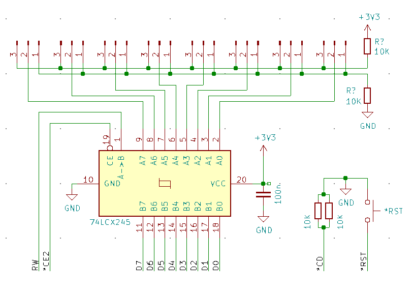
You want just the serial port ?
No problem, here a schematic that sum up all of above. You just need to plug a cheap serial TTL/USB and you are good to go.
![]()
Next steps
As stated in the "history" logs and in the project summary, I did all that research to satisfy some needs of modern connectivity.
Am currently working on the design of a prototype for a card with USB, WiFi and Ethernet connectivity.
For the USB I'll be using a real FT232RL. The cheap alternatives are good but I want to have an unique serial number to allow my computer to do some automation when I plug the scope (udev rule to have a /dev/tds3014 symlink ;) ).
For the WiFi it'll be an ESP32 module with a pigtail antenna to get the signal outside the scope. I don't want the WiFi to alter the poor FFT frequency analyzer or create any kind of artefacts. Better be sure than sorry.
For the Ethernet, a LAN8720A added to the ESP32. The project wESP32: Wired ESP32 with Ethernet and PoE confirmed it's usable and it's creator made a wonderful job with it. With no shame, I'll learn from what he did.
Even if now we have full access to the serial port it's still SLOW to retrieve a screen capture, even at 38400Bps !!! So I'am adding a 328p to act as a printer emulator as there is not enough remaining GPIO on the ESP32. I don't know for the moment if it will act as a master or a slave, but probably the first if I can.
I'll have to do some programing. It'll be a real challenge as I never really programmed something harder than plugins some libs to use some RGB leds, talking with I2C or SPI slaves. And I'll have to learn again a bit of C/C++, and probably ASM for the 328p to get the correct timings.
The schematics are done. The Ethernet part is "nearly done". I need to check again for proper grounding, decoupling, bulking and impedance for the differential tracks. But before completing it I need to learn a bit more about crystal oscillators and how to prevent interference from them. I found a lot of resources, but some are conflicting.
I'll keep this log updated time to time.
A little end note for this log.
stas_last created a program for an ESP32 to retrieve the serial prints from the scope on a browser. I don't know if he have a GIT for it, but, you can find the archive here : https://www.eevblog.com/forum/testgear/reverse-engineering-tektronix-tds3gv-module-for-tds3000-series-oscilloscopes/msg3014688/#msg3014688
-
Success !
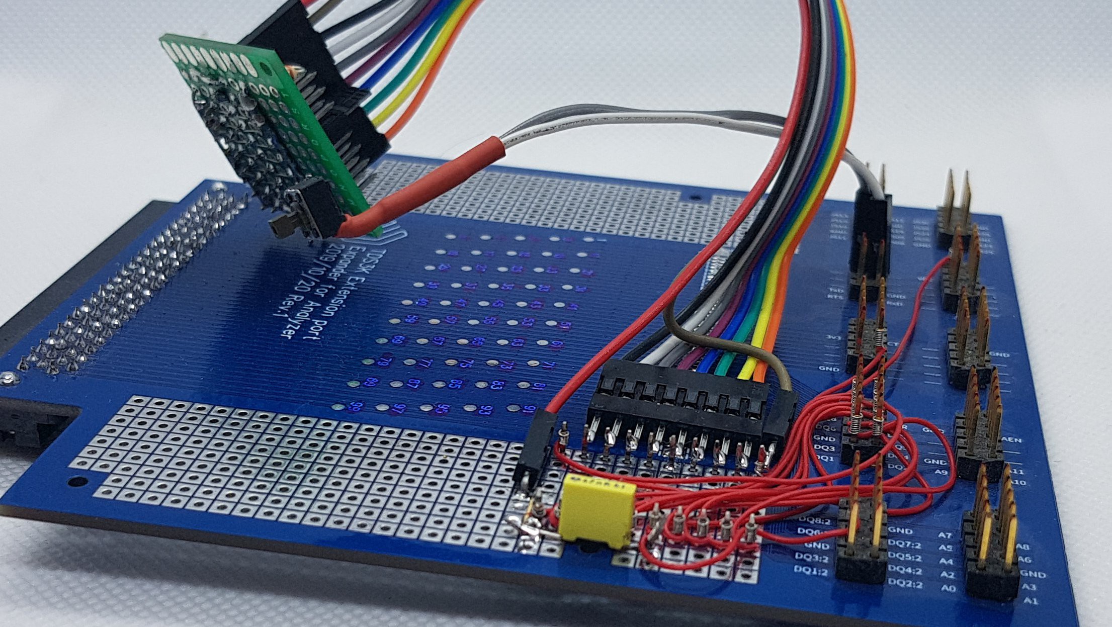
06/19/2020 at 20:56 • 0 commentsAfter some wire wrapping and soldering I had exactly what I needed to test the finding with this simple schematic :
Pretty simple, but it'll do the job.
![]()
![]()
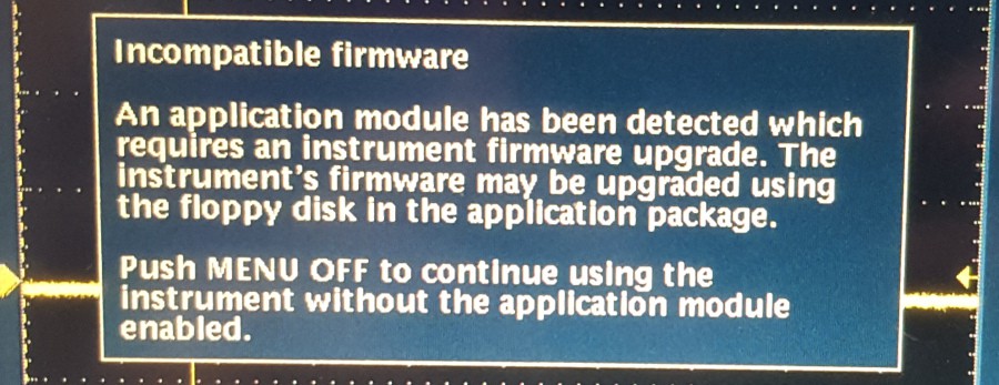
Until now, what I got with from the scope when pulling down the *CD pin was a message saying I had to provide a firmware update.
![]()
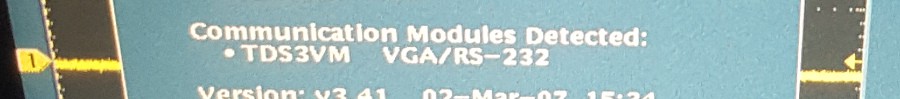
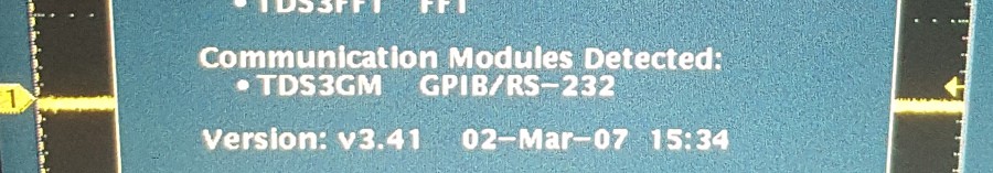
But now, what i get from this test card after testing with the jumpers is a "virtual" TDS3GV, a 3GM or even a 3VM !
![]()
![]()
Sweet as hell :)
Let's try an *IDN? command using the serial port.
![]()
Okay, it's working, even without a TDS3ENG key. Even getting a screen capture from the scope with a GPIB command is okay.
Seem like i can grab a beer and start writing a summary of what where found. -
It pay of !
06/18/2020 at 22:22 • 0 commentsTo keep it short : life is life. Demanding baby. Lot of time spent on solving problems at my job. Too much tired to work on my projects. But at lest i solved nearly all of the stacked problems at my job and my little boy gave me some space.
So 6 weeks ago I FINALLY had free time and ENERGY to get back to my projects ! YES !
Being far from it for some time wasn't bad. When I looked at my notes (and after a lot of hours of looking at others videos / projects) it was clear. I missed/ignored one important information I read when starting this project.
The CPU !!!! The CPU have two PCMCIA bus to manage extensions. How could I've missed that ! I felt stupid, angry, overjoyed and on fire all at the same time...
After studding how the PCMCIA bus work, I understood more about the board and it's schematic. I had guesses some lines correctly, some other seemed strange, so more guess until it felt coherent. So more pins where identified.
There's a card detect signal. During previous my tests (didn't write them down in the buildlog) i found that pulling it down to GND with a 5K had an effect on the scope. It detected that a card was inserted but it was unable to detect it correctly. Now I know it's just on step to the card detection.
All of the data pins and data lines I identified previously left me with doubts. After reading the CPU documentation, I knew why. All the address pins are swapped. The CPU is BigEndian and the PCMCIA is LittleEndian. And more than that. the address lines for the PCMCIA is shifted by 6 bits. The CPU as 32 addrs lines, but only 26 for PCMCIA. CPU A32 is PCMCIA A0, and CPU A6 is PCMCIA A25.
Now I knew. I knew how the card was identified. One LCX245 act as a 8 bit ROM mask connected on the D0-D7 bus and selected using /CE2 and R/W signals from the PCMCIA bus.
But no LCX245 in my stock. Had to buy some.
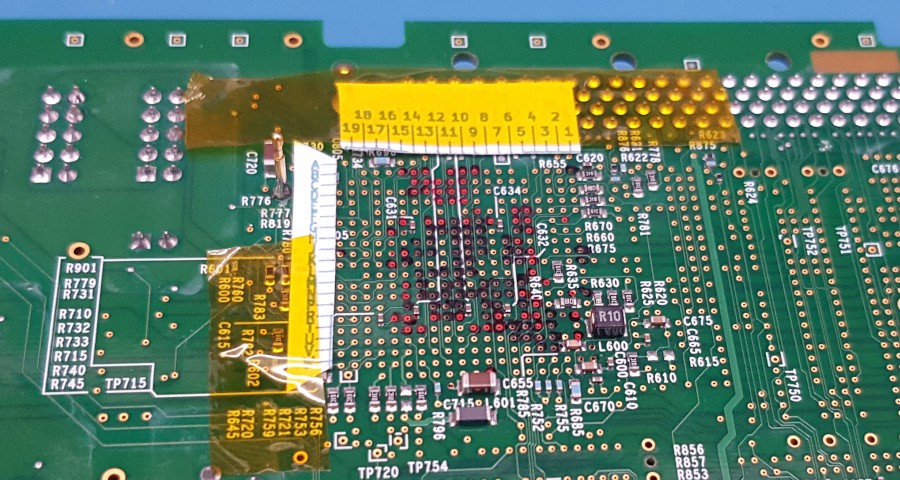
Waiting for them I got my 3032C, opened it, put the mother board out, more paper, more pen, made a tool to probe a large area on the mother board, and it was a stop. The vias under the BGA package are a mess. Not aligned with the pins, missing holes, .... cold shower. I already knew it, but I forgot.
![]()
After a good night of thinking instead of sleeping, I decided to do the inverse. Why not probing the vias with the pins i already know from the expansion port ?
After pocking around like that a pattern started to emerge on the vias. Some lines was just pushed left or right, other top or down and even in diagonals.
The CPU as a lot of GND pads, all in the center. A black sharpy, and all pins connected to GNDs was marked. A red sharpy, and all VDD pins marked.
Time to poke around more and get the exact position of each pad on a paper. Every pins identified is marked with the sharpy. It helped a lot and more pins were identified or corrected on the expansion slot. And like always, more paper ...
![]()
And then.... three weeks ago the TTLs arrived.
-
Keep looking, keep drawing !
06/18/2020 at 20:24 • 0 commentsI had a lot of problems and familial events. I abandoned this project. Too much to manage, too much problems to solve. I had to cut a drop whatever was not absolutely essential.
.... time passed and i was able to get my head out of the water. Getting back at my bench I saw the two scopes who were waiting looking at me with their lonely buttons. I abandoned a project i had with them. Still had plenty problems to solve, but why not looking at it just to be sure i made the good choice.
I won't go in details as it can be pretty boring, but i was more the type that do everything by himself. All the recent events in my life got me to reflect a lot on myself. So i tried something I had never done until now : Getting some help !
So i looked for people that had extensions cards and who were kind enough to share a scan or a photo of their cards.
Two days later, success ! Someone accepted to help me. He had access at his job to the extensions cards i needed.
He sent me a lot of photos of the cards he had. Front, back, top and down. I can't thank him enough for that. He got me fired up again about this project.
As i had to take a temporary leave from my job, all of the problems linked to it disappeared (nearly 75% of them). I had some brain time to spare for my own projects.
First step was to look for software who reversed or helped to reverse a PCB. Or at least some techniques. I learnt that some company are specialized in this field, that some windows program helped in this, some searcher published papers about reversing a PCB with computer vision. I don't have money, I don't have/want Windows, i didn't want to start learning another domain for the moment.
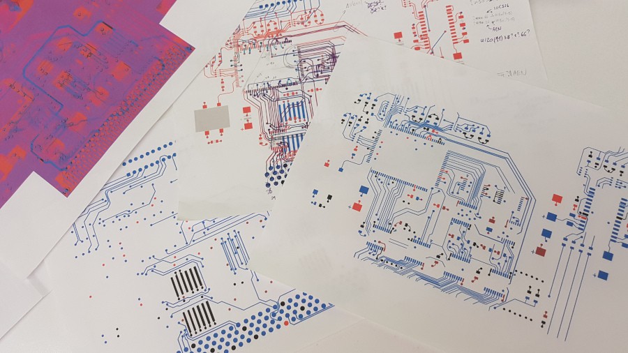
So it was a fallback to what i already knew and had : Gimp and a good old Wacom tablet.
![]()
What i learned for my first PCB reversing 4 layers board with trials, errors and looking for what other people do :
- Get the best and more detailed photo you have for each side of the board.
- The best photos are with homogeneous lighting
- Play with the colors/contrasts/highlights/gamma/filters to get the best view of the copper tracks
- Learn how to use the cage deformation tool
- Create a layer with a specific color for
- the top traces (light red)
- the bottom traces (light blue)
- the components (light grey)
- For every vias, look for the thermal relief, it a good hint to know to what layer it's connected
- Use a hard pen, not a brush to draw over the tracks. For the width, 5 to 9 pixels was enough for me.
- Try to leave some space between the tracks you've drawn, ti's easier to read after
- If you spot the a VCC rail, a GND rail or any power rail, mark it with a specific color
- Even if you don't need a full reversal, it's useful to correctly all the tracks
- Real paper and real color pens are still the best tools :)
Okay, i had most of the TDS3GM board tracks. And I though, good job, i'll find how it work by tomorrow for sure.
Silly me. It's where the real hard work start !
I knew how to use EasyEDA, but it left me with a sensation of playing with a baby toy. So it was time to look for something more robust. A long time ago I played with EaglePCB, but the licensing and limitations where pretty frustrating. I wanted to really get into electronic hobbies, so knowing i can get stopped because i used something like that ... naaaahhh. So after some googling, youtubing, reading, benching and accounting i choose KiCAD to draw the board schematic.
I'll keep this part short as the "history" of this project is near it's end. Not because i don't want to share any useful technics or information, but because i don't remember all i did. That a shame because it's in theses part that i spent a lot of time understanding what was going one on this simple design and learned a lot too in the process !!!!
Here what i can share for sure is :
- reverse engineering a 4 layer PCB just with photo is a lot of recursive analysis
- Even with missing or interrupted tracks you can guess where they are going to using datasheets and trying to understand how the board was designed
- Sometime if you can't find where a track is going, take a guess and way to see if it match with the other guesses/tracks
- Having your cleaned tracks printed on paper allow you to easily take notes, so don't reject paper, love them :)
- It felt easier to follow a track with a pen on a paper
-
More pins, more serial and a wall
06/17/2020 at 22:24 • 0 commentsBefore going to the serial port subject, I took some time to analyze the display pins.
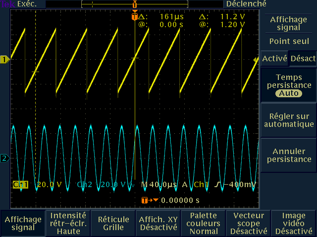
The clocks were easy and matched what I found about some simple color LCD datasheets
- DotClock : pin 2 (25MHz, 50% duty cycle)
- HSync : pin 3 (31.5KHz, 88% duty cycle, 31.72µs high and 3.82µs low)
- VSync : pin 4 (60Hz, 99.6% duty cycle)
The colors bus needed more work to distinguish the good colors and what pin were what color bit as it was impossible to see them on the photos of the board.
I had to play with the color schemes and the signal intensity to see emerging patterns to find the bits of each colors :
- Red[0-3] : pins 6 to 9
- Green[0-3] : pins 51, 52, 54 and 55
- Blue[0-3] : pins 56, 57, 59 and 60
That done !
Now back to the serial port.
Yes, it's bugged me.
I came to the conclusion that i needed to force the scope to detect a "virtual legit card" with a serial port and a GPIB.
After some more time contemplating the board photos, it made sense that the TTLs had a role to play with that but no way to confirm it without a schematics of the board. It was at that time I sawn a wall. The photos where not clear enough to extract correctly the traces.
But came another EEVBlog member who gave me an important information : enabling the TDS3ENG application module activate the serial port !
Some more I2C programming, and i had the serial port activated !!!!
But ... it didn't respond to any GPIB commands !!!!
Bah at least I can now use the serial port to print the screen to my PC with a little quick and dirty python script.
from serial import Serial
from time import sleep
from time import time

s = Serial(port="/dev/ttyUSB4", baudrate=38400)
wait = -1
with open("dump.png", "wb") as f:
    while True:
        data = s.read_all()
        print("%s : Received %u ... " % (time(), len(data)))
        if len(data):
            f.write(data)
            wait = 3
        elif wait >= 1:
            wait -= 1

        if wait == 0:
            exit()

        sleep(1)
many seconds later ... it's slow even at 38.4KBps
![]()
Even if i still need to find a way to simulate the presence of a card, i can now slowly print a screen capture to the serial port if needed.
-
First PCB
06/17/2020 at 21:46 • 0 commentsI had the connectors, but what to do with connectors. Last time I checked, they are used to connect things together...
For the next steps I needed to extract the bus connector outside the scope to play with it.
So let's do a testing board as my very first PCB. Seemed easy to learn the routing process as there was a lot of tutorials and resources.
EasyEDA was a good candidate to start with. I had one problem to solve that got on my nerves : the connector was unknown in the library. I had to import it myself from mouser or other. It was a pain as am a Linux guy and whatever i found used Windows to do so. Wine wasn't a big help. I had to create a Window 10 VM just to import one connector inside EasyEDA. But in the end i had the connector in the EasyEDA shared libs.
Many iteration of the board later, many hours of learning by trial and errors, many hours of looking resources about making a good digital board, i had a board to convert the 100 pins connector to 10 x HE10 headers plus prototyping space and exposed signal traces to solder on if required.
![]() 3 week later, some soldering, and it was now the time to get on the scope screen what was going on inside himself.
3 week later, some soldering, and it was now the time to get on the scope screen what was going on inside himself.
But first, I had to test the serial port again :)![]() It feel safer to work and poke inside the scope.
It feel safer to work and poke inside the scope.
Oh and it worked like a charm. Happy with my first PCB and ... gave me the need to make more PCB like that ... my wife will hate me sooner or later ...
Serial work but still no change for the *IDN?.
PS: Later on I found that i made errors with the annotations on the card, but too late, it was sent i production. A least the headers pins are numbered correctly. -
Reversing the expansion pinout
06/17/2020 at 21:25 • 0 commentsTime to get out the continuity tester and crack open the scope a second time !
As I knew where the power rails where in the scope, so the best and quick way to narrow the pins :
- GND : 1, 5, 10, 21, 32, 38, 45, 53, 58, 67, 80, 86, 91 and 96
- 3V3 : 12
- 5V : 72
Next steps was to find the datasheet for the RAM/FLASH chips on the main board and use them to find address/data lines :
- Data lines : 82 to 100 (minus GND lines)
- Address lines : 37 to 50 (minus GND lines)
- R/W : 70
Yep, seemed legit, they were facing each others on the same side of the connector.
Then, how does the scope send the screen signal to the board. A bit of pocking around got me to the J500 connector of the LCD. Nearly all LCD have at least a select line, a dot clock, a line clock, a screen clock and color lines. More pocking around and i had what seemed the clock lines and the color lines.
Some time after, another user mapped the serial port pins from his own card and kindly shared them. They was around where i expected to find them, but ... oh no ... pins 70 were RTS signal for him. I had to check again all of my mapping.
He was right ! My notes where done on a single paper, with annotations everywhere. So news lessons learned from error :
- when writing down pin out, make a table that match the positions of the physical pins
- add enough white space to take your notes
- use colors to discriminate your assumptions, what need to be verified and what was right and wrong
- after every sessions, update a second table with only the correct pin map
Some day later the male connectors for the expansion slot arrived. Time to test the serial port with a cheap TTL/USB converter.
![]()
Some week earlier I buyed a non working TDS3032C for 100€ i wanted to use to get the full pin out and some spare components. But after testing it i found that i just have a scope with a non working main power supply, but that can run on a battery pack. I though it would be best to use it to make my tests.
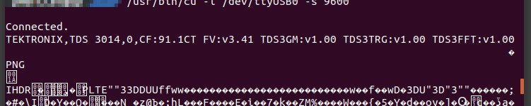
Connecting the new serial cable in the scope, launching a terminal emulator, typing and sending
*IDN?
and was answered by a long awaited
TEKTRONIX,TDS 3032C,0,CF:91.1CT FV:v4.05 TDS3FFT:v1.00 TDS3TRG:v1.00
That was good, but next was my TDS3014... and it didn't work ... Why ? My firmware ? My extensions ?
Can downgrade my TDS3014 to an older version. I have working floppy drives, but no working floppy disk anymore.
I have on oscillo that work with the serial cable it's enough to know the only thing that limit the serial port is the software.
-
Finding references
06/17/2020 at 19:52 • 0 commentsFirst, as a good practicer and enforcer of the RTFM principle, I looked into the service manual of the scope. What i found was interesting, how to test the main board and power supply : where is GND, 3v3, 5V and 12V rails.
Except for that, nothing really useful for my project.
Second, using the published photos of the TDS3GV found on the EEVBlog forum, the ref for the chips were easy to get. An unknown connector, some TTL, a VGA driver, a classic MAX232 and a GPIB controller. Easy to see how it work:
- 7 x 74LCX245 Tri-states bidirectional transceivers
- One 74LC00 quad NAND and one 74LC08 quad AND, probably managing the address selection for the chips
- One ADV7120 probably for driving the VGA port plus it's impedance matching components and bypass capacitors
- One classic MAX238 for the TTL/RS232 serial port plus some caps for the integrated step-up
- A big chip labelled TNT14882 who seemed like a GPIB controller/driver with filtering caps and inductances for the GPIB lines
- A 40MHz quartz
- Some caps, resistances, ... don't know why
- An unknown 100 pins connector
The block diagram of the cards was easy. Next, finding all of the chips datasheets.
TTL chips : no challenge. But i didn't know the LCX familly. To summarize : it's the family of 3v3 chip, with low noise, high speed and 5v I/O tolerance. I'll keep them in mind for sure.
ADV7120 : a sub 15$ 5V driver to transform 3x8 bits colors to a proper VGA signal. Good guess and the data sheet confirm the impedance resistors. But .... it seem the scope use only 4bits per colors ... will have to check that.
MAX238 : Same here, no challenge. But can't find the expansion port pins just by looking at the photo.
TNT14882 : This one was ... tricky to get. The only information i could come across was a commercial brochure that confirmed it was a GPIB controller. The National Instruments had the full datasheet but ... like always, when you need old information, you can't get it because it's too old and someone removed the file on the web server ... I was doomed. Some time later I found this datasheet in a dark corner of the web on an anonymous FTP. Don't know who put it here, but you have my thanks !
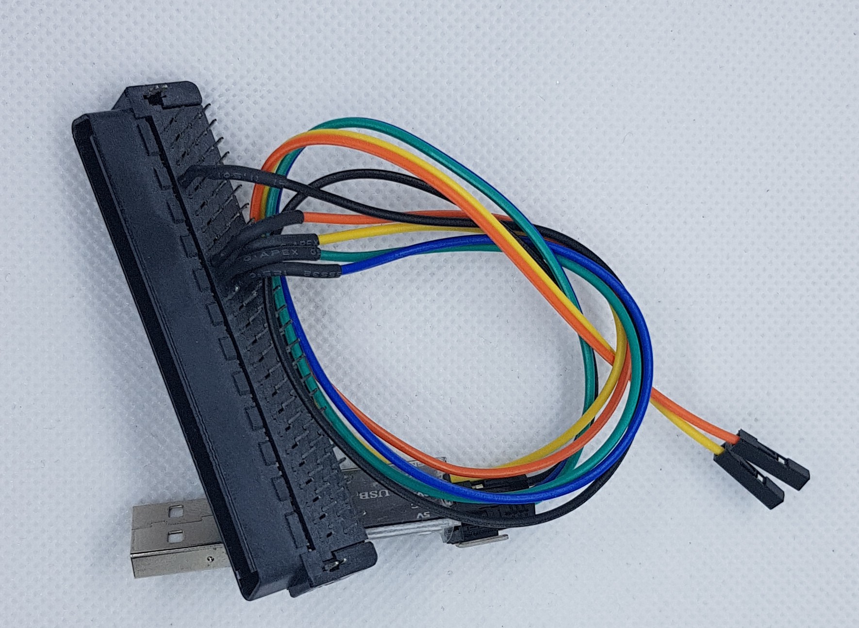
For the unknown expansion connector, i had what i need just in front of me : the matching female connector. Time to get the caliper and some drawing paper. After all measurements and a lot of mouser browsing i nailed it : AMP 1-1734099-0
![]()
A note about the measurements : If i can't put my hand on cheap connectors (Mouser, Digikey are a no go for me : VAT and import taxes add 40$ on every commands) i will be able to make my tests using a 1.6mm PCB with 1.27mm spaced tracks. It match the female connector perfectly ! But i would prefer using the male connector for reliability and longevity especially for some Rev&Dev.
Luck was here, as some days later, someone sold there old stock on ebay : including shipping, 25$ for 11 connectors. Lucky me !
Extension card for TDS3000 scopes
TDS/3K32 Network and serial interface card for old TDS3000 scopes.
 3 week later, some soldering, and it was now the time to get on the scope screen what was going on inside himself.
 It feel safer to work and poke inside the scope.