 kamalkedin123
Term Programmable Peripheral Interface (PPI) is used for the integrated circuits that interface / connect the external world to the central processing unit (CPU). Generally, a variety of programming modes are provided with the IC.
8255A is a general purpose programmable peripheral interface I/ O device for Intel microprocessor. It has twenty-four I/ O pins which can be individually programmed in two groups of twelve and can be used in three different modes.
Features of 8255A-5
- 24 programmable I/O pins
- Completely TTL compatible
- Fully compatible with intel microprocessor families
- Improved timing characteristics
- Direct bit set/ reset capability
- Reduce system package count
- Improve DC driving capability
Replacement Part
MSM82C55A-2
Pictorial View
Pictorial view of the UTsource 8255A-5 is shown below and price can be found; it is a forty pin DIP package

Pin Description
Pin description of the IC 8255A-5 is shown below

Pin Number | Pin Name | Description |
34 - 27 | D0-D7 | Data bus |
6 | /CS | Chipset |
35 | RESET | Reset |
5 | /RD | Read control |
36 | /WR | Write control |
8 – 9 | A0-A1 | Port address |
4 -1, 40 - 37 | PA0-PA7 | I/ O port A |
18 - 25 | PB0-PB7 | I/ O port B |
10 - 17 | PC0-PC7 | I/ O port C |
7 | Gnd | Ground |
26 | VCC | Power supply |
8255A-5 Electrical Characteristics/ Specifications
Parameter | Description | Value |
TSTG | Storage temperature | -65 to 150 C |
VPIN | Voltage on any pin | -0.5 to 7 V |
PD | Power dissipation | 1 W |
VIL | Input low voltage | -0.5 to 0.8 V |
VIH | Input high voltage | 2.0 to VCC |
VOL(DB) | Output low voltage on data bus | 0.45 V |
VOL(PER) | Output low voltage on peripheral bus | 0.45 V |
VOH(DB) | Output high voltage on data bus | 2.4 V |
VOH(PER) | Output high voltage on peripheral bus | 2.4 V |
ICC | Power supply current | 120 mA |
IOFL | Output float leakage | ± 10 µA |
IL | Input load current | ± 10 µA |
Working Principle
8255A is a PPI designed to interface microprocessors manufactured by Intel. Its main function is interface general purpose I/ O components with the system bus. The functional configuration of the 8255A is programmed by the system software so that normally no external logic is necessary to interface the peripheral device or structure. A table explaining the basic operation of the 8255A is given below
A0 | A1 | /WR | /RD | /CS | Input Operation |
0 | 0 | 1 | 0 | 0 | Port A to Data Bus |
1 | 0 | 1 | 0 | 0 | Port B to Data Bus |
0 | 1 | 1 | 0 | 0 | Port C to Data Bus |
Output Operation (Write) | |||||
0 | 0 | 0 | 1 | 0 | Data Bus to Port A |
1 | 0 | 0 | 1 | 0 | Data Bus to Port B |
0 | 1 | 0 | 1 | 0 | Data to Port C |
1 | 1 | 0 | 1 | 0 | Data Bus to Control |
X | X | X | X | 1 | Data Bus to 3 State |
1 | 1 | 1 | 0 | 0 | Illegal Condition |
X | X | 1 | 1 | 0 | Data Bus to 3 State |
Applications
General purpose programmable I/O device for Intel Microprocessor
Keyboard and Display Interface
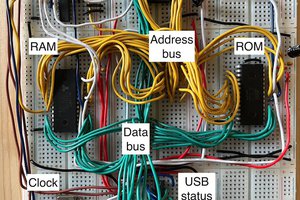
A keyboard and display interface using P8255A is shown in the figure below

Printer Interface
Pinter interface using 8255A PPI is shown below


 Stephen Willcock
 Keri Szafir
 DAB-Embedded
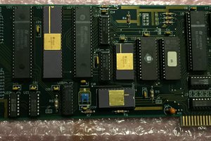
 Keith
Keith
Oh man, this chip was so long ago. I've got a pile myself. Why not feature a more modern chip people are more likely to use like the MCP23017, an I2C to GPIO chip?
And why is this a "completed" project? You haven't done anything except quote the datasheet, which talks about parallel keyboard and printer interfaces.