Bharbour
-
More Thoughts on SPI vs I2C Drivers
12/24/2020 at 16:18 • 0 commentsIn the previous log, I talked about the system problems with the ISSI driver chips that use an I2C interface with limited (4 devices per bus segment) address choices. Also mentioned are the daisy chain aspects of the SPI interface using the expensive MAX7221 parts. Possible solutions for the limited address choices in the I2C chips are:
A) Use multiple I2C buses.
B) Use address translators to break up the I2C bus in to multiple segments.
C) Use I2C bus multiplexers to break up the I2C bus in to multiple segments.
Option A works if you only need a few characters displayed, or the MCU that you are using has multiple I2C buses. The SAMD21 parts in the 100 pin packages give you access to up to 6 I2C buses which would drive up to 24 characters of the single driver version of the IS31FL3730 chips. Managing 6 I2C buses and splitting up the outgoing character data would be a hassle in the software part of the project, but could be done.
Option B, using address translators to break up the I2C bus in to multiple segments. Linear Technology/Analog devices makes some address translator parts that allow you to XOR bits in the address field of an I2C packet on an isolated sub-bus. The parts that I have used are the LTC4316 (single and LTC4317 (dual) multiplexers. This arrangement works pretty well, I used the LTC4316 parts on the IS32FL3738 based driver boards. The advantage with the translater chips is that you get maximum flexibility on the addressing by using them. If you select your addresses carefully, the fact that the bus is segmented downstream is invisible to the bus host.
There are a couple of problems with them though: cost, build complexity and limiting your configuration options. The LTC4316 parts cost $3.61 US each, and will allow you to add 4 additional IS31FL3730 based boards. The original IS32FL3738 boards that I built had two of the driver chips and one of the LTC4316 chips per board. This is an expensive board when you need several of them. Later, I built a dedicated bus splitter/translater board that used two of the LTC4317 chips per board to get up to 4 separate bus segments with their own address translation. The LTC4317 chips cost $4.34 US each, and can support up to 8 of the IS31FL3730 based boards per translater chip.
Both the 4316 and 4317 parts use external resistor dividers to set the bit combinations to XOR with the address fields. There is one divider to set the lower 4 bits of the address and another divider to set the upper 3 bits of the divider. The resistors used in the dividers need to be 1% resistors to have a deterministic mapping with manufacturing tolerances. Each extra sub-bus adds 4 additional resistors to the board design, configuration and assembly time. For manual assembly, keeping all of the resistor values straight and getting them in the correct location adds to the build time of an otherwise low component count board. I wound up writing a C program to generate a table of the resulting address maps with the resistor combinations.
The data sheets offer specific values for the resistors to select the XOR bits. The values shown are fairly high resistance. I thought about designing the splitter / translater boards to use jumpers to select the resistor values, but was concerned about spreading these high resistance dividers around on a board with jumpers to get configurability. For the first generation of driver boards that each had their own LTC4316 on them, the PCB real estate required to add a jumper system in a noisy digital environment was prohibitive. The resistor configuration system is not a binary system, so controlling 4 bits of address configuration would require up to 16 jumpers.
Option C, using I2C bus multiplexers to break up the I2Cbus. Initial searches for I2C bus multiplexer chips showed only expensive parts, and using bus multiplexers requires some software support. I dug around some more, and found some low cost 8 channel I2C bus multiplexer chips, the PCA9547 from NXP. The PCA9547 parts cost $1.78 US. One of the PCA9547 chips will support up to 32 characters using the IS31FL3730 driver chips. The required software support to use the multiplexer is minimal. I wrote a function that will issue a command to change the multiplexer setting if the sub-bus number changes in the communication process. An additional array was added at the lowest level of the software that contains the sub-bus number for each character. There is already an array containing the I2C address of each module, so the extra array and function call is a minimal effort.
At this point, Option C is going to result in the lowest parts cost and simplest cabling for projects with more than a few characters.
The splitter / multiplexer board that I designed also got an I2C ambient light sensor stuck on the back side of the board. In use, the new splitter / multiplexer board will sit next to the row of LED character modules, with the ambient light sensor facing outward. The ambient light sensor was used in my GPS clock project to automatically set the LED brightness based on room light levels, and I am very happy with that feature.
One of the positive aspects of my exploring the other SPI interfaced driver chips is the idea that I had of daisy chaining the display driver boards with pass through connectors. The clock project that I built did not have the pass through connector setup and the cable that bused 9 characters of an I2C bus was pretty painful to make. Redesigning the IS31FL3730 boards to use the pass through connector arrangement will simplify the cabling a lot. Limiting the I2C sub-buses to 4 characters each will also limit the power supply current through the pass through connectors.
-
Yet Another Driver Board to Play With
11/20/2020 at 22:43 • 0 commentsSpeaking with someone here on Hackaday, they mentioned that they were planning on using a Maxim MAX7219 chip for driving these displays. Out of curiosity, I decided to build a few boards to explore this chip. Perusing the data sheet, the MAX7221 looks like an updated version of the 7219.
Using these parts to drive a matrix LED is a little bit of an "off label" use. The data sheet talks about using these parts to drive up to 8 of the seven segment numeric displays, and not much about driving a matrix display. There is even a BCD to seven segment translator built in to the chips. On further reading, the translator can be bypassed, and the chip is designed to drive common cathode displays. The LTP2558 matrix displays that I have are common cathode displays.
These chips use SPI for communications instead of the I2C that the other two driver chips use.
With the I2C based chips, the target address specifies which chip on the bus that you are talking with. The ISSI chips that I used only support 4 different addresses, meaning that if you want more than 4 characters in the display, you have to break up the I2C bus. Address translators or bus mux chips are the two most obvious ways to do this. Either is expensive. Another method would be to use a controller with multiple I2C buses. This seems wasteful of resources, and adds cost, as you need to buy a higher pin count processor.
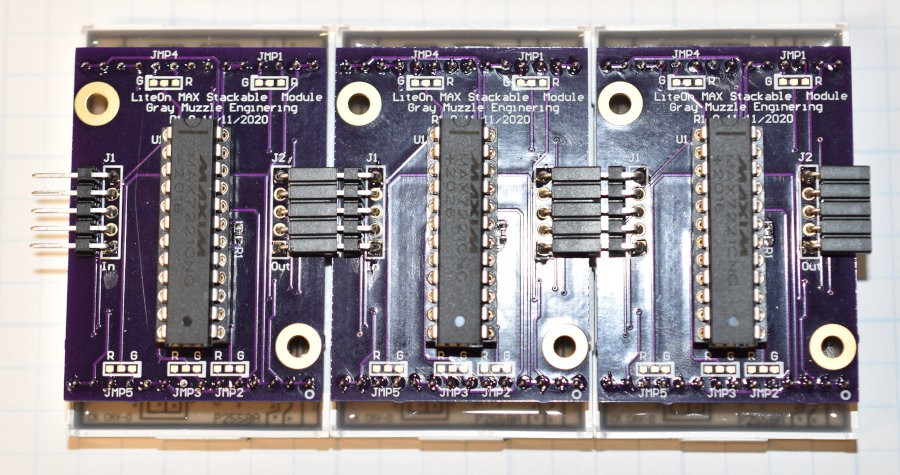
The SPI interface uses daisy chaining to build a bus up, and the physical order that you put the data on the bus determines which driver chip winds up with a particular word of data. As a result, there are no addressing limitations created by the SPI interface. There are some limits to how many devices can be put on a chain. There may be timing limitations since all the parts use the same chip select and clock signals to pass and store data. There are bus loading limitations, as it is necesary to drive the clock input and chip select input of every driver chip on the chain. Because of the higher data rates supported by SPI interfaces, expect to have to terminate the SPI bus to preserve signal integrity.
The biggest advantage that the MAX7219 or 7221 chips bring to the hobby world is that they are available in the old school DIP package, a 24 pin skinny DIP with 0.1" (2.54mm) lead pitch and 0.3" (7.62mm) spacing. These packages are very easy to solder without microscopes or other special tools and skills. They are also small enough to pack two of them on a board that sits on the back of the LTP2558 displays.
The biggest problem with these chips is that they are expensive. The 7219 chip lists at $8.91US and the 7221 chip lists at $9.26US in single quantities. The pricing does not fall very fast on the volume curve. Searching the net, some sites are offering the MAX7219 as cheaply as $1, but if it sounds too good to be true, it probably is.
Writing a driver for these chips is somewhat different than the I2C interfaced chips. With the I2C chips, you could write all of the On/Off control registers of one driver chip in a single I2C transaction. With the SPI interface, you can write one of the control registers of each chip on the chain in a single transaction, necessitating breaking up setting the LEDs into a transaction per display column. After some testing, you HAVE to write each chip in the chain every transaction or strange things happen and downstream characters get corrupted.
Both the I2C and the SPI device drivers use a character generator table to map the incoming ASCII character to the desired pattern of LEDs. The character generator table used for the MAX parts is identical to one of the ones used in the ISSI31FL3730 driver that I already have written. The MAX parts run 5 columns X 8 rows of LEDs in the matrix. The character generator table supports 96 different characters, one for each of the printable ASCII characters. A 2 dimensional array with 96 x 5 bytes holds the character generator table data. When the ASCII data array comes into the device driver function, it is translated into an array of pointers for the character generator table. Each incoming character becomes a pointer into the correct location in the character generator table for that character. A nested loop assembles a column register address and the correct column data for each character into a transmit buffer. At the end of the inner loop, the transmit buffer is sent out to all of the driver chips in the chain. The outer loop iterates until all 5 of the columns for the characters have been sent. This is considerably more complex than the I2C driver.
One "feature" of the SPI chain is that the first byte out of the bus controller winds up in the last driver chip in the chain. This means that the physical SPI chain should run from right to left through the driver chips so that the first character data winds up in the leftmost driver chip. Obviously, it is possible to reverse the order in software, but the driver is already complex enough.
On the previous driver boards that I designed, there is a single connector for the power input and the I2C bus. This required making a messy cable with a tap for each character. For the new boards, I pass the data through the boards with an input connector and an output connector. The boards will stack side by side for the length of the chain with no cable between the displays. This method reduces the flexability on picking the character to character spacing though.
Each LTP2558 display has a separate red and a green 5x8 matrix. I designed two boards using a single MAX7332 chip with jumper selection for the color. Personally, I like the green better, so I made a default connection to the green matrix. If it were necesary to run the red matrix, the jumpers can be cut and the red selection made with a soldered in jumper. I don't think it will be possible to run both the red and green matrices at the same time, from the same driver chip. The forward voltage of the red and green LEDs is different enough that the green LEDs would probably not be visible at the operating voltage of the red LEDs. This has not been tested though.

Front View of first Daisy Chained design. 
Three of the Modules Daisy Chained After having the first version of boards to determine the inter-board stacking distance, I did another version that stacks the boards in contact with each other. This will require a new driver methodology to drive. The character generator arrays used on the other displays take advantage of the ability to space the characters with the display module mounting. The driver system is completely character oriented. One characters data goes to one LED module. The non-spaced modules are a continuous array of LEDs. To take advantage of the non-spaced LED display system, the driver is probably going to look more like a video frame buffer.

Three of the Non-Spaced Modules Daisy Chained Together The internal organization of data in the MAX7221 chips is by LED column, so the "continuous" scan path becomes the vertical column. Video Systems generally have the scan path horizontal. If you look carefully at the edges of the display modules, you can see mechanical keying notches to help align the modules when they are in contact with each other.
![]()
Both of the board designs shown above only support a single color, defaulting to green.
A final iteration of this driver board will probably have extra connector sites so that the same PCB can be built as either a non-spaced board or with mechanical spacing between the LED modules.
In order to support the three possible colors, I laid out another driver board with two MAX7221 parts, one for red and one for green. The option to drive either or both red and green, 2 of the MAX7221 chips are needed. This gets expensive quickly. I did not use the plug pass through method on these boards because the power supply current can get pretty large with the possibility of running both matrices at the same time. In testing, I have seen 400mA per display in some situations and the pass through connectors are only rated at 3A per pin. Also, the power ground and the SPI ground share a common pin.

Driver Board using two MAX7221 chips to control Red and Green matrices The SPI cable interconnect arrangement is showing some signal integrity problems and requires a terminator at the end of the cable to get reliable communications. Neither of the PCB daisy chain designs required termination to operate reliably, though that may change as the number of modules on the chain increases.
-
Ported the driver code over to the Single Driver display modules
09/26/2020 at 21:56 • 0 commentsMost of the work on the #GPS Driven Clock project is done. It is presented as a separate project.
As mentioned in earlier log files, the dual driver display modules were too expensive, so I developed driver board using a different driver chip (ISSI IS31FL3730) that is about 40% of the cost of the dual driver modules. When I started on the clock project, I had just gotten the first of the single driver modules built up and minimally tested.
This morning, I built up the other two PCBs for a total of 3 of these displays operating. In order to drive the new displays with more than just test code, I ported the software drivers over to deal with the IS31FL3730 chip. The architecture of the new chip is quite a bit simpler than the previous one, so the initialization sequence changed and there is only one chip per module to drive. Because of the way that the display had to connect to the driver chip, the data format for the green LEDs is rotated 90 degrees from the format for the red LED data. I brute forced this with a second character generator table rather than rotatating the data in real time. The character generator tables are 768 bytes per table, which is not too ugly.
The current control register on the new chip is a wierd, discontinuous thing, so I need to write the code to map a linear input value to the required register data format. 10/5/2020 The current control function is written and the display drivers are willing to source up to the 70mA listed on the data sheet. They run kind of warm when doing so though.
The new chips only support 4 different I2C addresses, and I did not put an address translator chip on each board, as the translator chips cost more than 2X the cost of the display driver chips. I have a bus splitter/address translator board laid out already that will let me run 4 separate bus segments with their addresses mapped to unique spaces, so one of those boards will support up to 16 display modules. Also, the power for the displays and the power for the address translator chips are supplied through different connectors on the splitter translator board. This will allow me to run the I2C bus on the microcontroller side at 3.3V and the individual I2C buses to the displays at 5V which should give more headroom on the LED supply from driver chips.
10/8/2020 The boards for the I2C Splitter/Address Translator are back. I built the first one up and verified that it is operating as expected. I need to order some more connectors to finish it. Also, it won't be required until I build up more of the single driver displays.
-
The Boards Are Back
08/27/2020 at 12:39 • 0 commentsThe last 3 of the rev 1.1 boards are back from OSH Park and assembled. The chassis that I designed for 9 displays is now populated and looks good.

Fully Populated Display Panel I started working on the application code for using these beasts while I was waiting for the boards to come back. It will be a GPS driven clock. I also built a breakout board for an ambient light sensor chip to use for automatically dimming the clock.
In the previous log file, I mentioned doing a PCB for a different driver chip that would be a less expensive board. After totalling the costs on the bill of materials, the new boards come out at about 40% of the cost of the rev 1.1 boards.
The new PCB design is a 2 layer board because there is a lot less routing with a single chip than 3 chips, and the heat sinking did not appear to be the problem I was expecting on the original design. Using only 2 layers reduced the cost of the PCB by 50% . A single jumper wire was needed to route one signal on 2 layers, so that one blue wire is a feature, not a mistake :)
Prototype boards for the new design came back from OSH Park and assembled easily enough. I took care of several convenience issues with the new design like having jumper selectable address and terminator enable. To keep size down on the jumpers, I used the 1.27mm header and shunt blocks.

Component side of new driver board design 
Assembled display module. Because of the way the matrices of LEDs are implemented in the LiteOn displays, I had to rotate the matrix of the green LEDs by 90 degrees. The red matrix is wired as a common cathode matrix. If the green matrix had been wired as a common anode matrix, it would have matched the intended configuration of the IS32FL3730 chips, but no joy. The displays have two 5x8 common cathode matrices, one red and one green. I wound up connecting the red matrix in the conventional way and connecting the green matrix with the column driver outputs connected to the LED row inputs and the row driver outputs connected to the LED column inputs. This effectively rotates the green matrix 90 degrees. In use, the time penalty of rotating the character generator matrix 90 degrees while updating the display is probably more of a problem than the space incurred with a second character generator data set, so a second character generator data set with the data already rotated will solve that problem.
Rotating the matrix also has some implications about current control when multiple LEDs are lit in a single column, but that needs more testing to see if it will be a problem. I have a home written tool that allows sending I2C write transactions controlled by a simple text file with a lot of flexability. It uses the Total Phase Systems Aardvark to go from USB to I2C, SPI or GPIO. The tool called VarkBlaster is useful for exploring configuration and control of parts like this. I wrote a few scripts that drive the display with varying numbers of LEDs lit per row and per column, and there was no difference visible to me in the LED itensity.
Using the character generator array that I developed for the rev 1.1 IS32FL3738 based boards, I wrote a tool that translates that into the register bit formats for the two matrices in the IS31FL3730 chips and displayed a couple of characters from each array to sanity check it. So far so good. The character generator arrays form a lookup table mapping ASCII code to register values to display the character. In general, the brightness seems a little low but I have not started experimenting with the LED current control register yet.
-
Rev 1.1 PC Boards are Back
08/06/2020 at 17:58 • 0 commentsThe rev 1.1 PC Boards are back from OSH Park. I built up all three of them. They are much quicker to assemble since all of the components are on the top side of the board except the sockets for the LED Matrix.

Assembled Rev 1.1 Board I made sure to keep the bolt pattern and it's relationship to the LED Matrix the same as the rev 1.0 boards so they will both live on a mounting plate and be interchangable with the rev 1.0 boards. I also added resistors to support translating the low nibble of the I2C address that were lacking on the rev 1.0 boards.
I now have 6 of these boards built and operating, and I want 3 more. Those will be ordered this weekend.

Display Panel With 6 Modules Installed The cost on these modules is higher than I am happy with. Separate driver chips (IS32FL3738) are used, one for red and one for green. There are only 4 options for I2C address selection on these driver chips, so I added an I2C address translator to each board to allow running more than 2 boards on an I2C bus. The PCB is a 4 layer board. I chose to use a 4 layer board to get low impedance ground and power distribution to both display drivers and the address translator. Also, the driver chips have a heat spreader pad under them and I wanted to be able to use a ground plane for heat sinking the drivers.
Poking around in the projects on Hackaday, I found a project that is very similar to this one: #PIXIE - Chainable, Dual 5*7 Micro-LED Displays! The display driver chip (IS31FL3730) used on that project is capable of driving both the red and green matrices in the display, so I laid out a board to use that chip. These chips also support 4 choices for the I2C address, but only one chip is needed per board, allowing up to 4 displays on an I2C bus segment. I removed the I2C address translator and added jumpers to select the address and enable/disable the I2C terminators. My concerns about heatsinking the driver chip did not seem warranted with the rev 1.0 boards, the drivers only run a few degrees above ambient temperature. With a single driver chip to supply power and ground to, a 2 layer board makes more sense. With the changes listed above, the parts count is less than half of what the current boards are using, and it will go on a 2 layer board. To get the same functionality as the previous boards, either bus multiplexing or address translators are going to have to go into a system somewhere. A prototype board for the new driver is ready to send out to OSH Park.
The new driver chip handles the two matrices in kind of a strange way. One matrix connects to the driver pins labelled row[8:1} and column[8:1] matching the LED pin designations. This is a common cathode matrix. The second matrix looks to be a common anode matrix, but since both matrices in the LED block are common cathode, I rotated the second matrix, connecting driver rows to LED columns and driver columns to LED rows. It is not clear from the documentation whether the hardware corrects for this in the registers for the second matrix or not. I am just going to have to build one and mess with it. If the hardware does not correct for this, it will be necesary to do the pixel rotation in software.
It is not clear what the maximum LED current is for the new driver. The electrical specs in the data sheet say that the maximum is 40mA, but in the register set description, there is an option for 75mA. Running 40mA per LED may be enough, but that is another thing to test when the boards get back.
The IS31FL3730 uses my least favorite package for assembly at home, the QFN leadless package. None the less, it is worth trying. It is not like there is a deadline or anything.