Charlie Smith
-
Programing
10/14/2020 at 22:49 • 3 commentsSince the last log I have got the program card to be fully working, so the only incomplete parts to the computer are the input module and the clock. The input module still isn't a priority, and I will talk more about the clock below. I am now able to easily program the computer using my EEPROM programmer and a program card. So I can now start looking at areas to improve, as well as writing more complex programs.
The Stack
This is pretty much my first time using an assembly language properly, so while I could attempt to write some super complex program, it would be better to understand a bit more about how to write programs. Well there is a clear feature I should look into: the stack. The general idea is that we can store values in memory without having to allocate a variable in advanced. By using a stack data structure, we can either push a value onto the stack, or pop a value of the top (you can also peek to look at the top value without removing it). This is often compared to a tall pile of plates. You can either add one to the top or remove one from the top, you can't remove one from the middle (without being very careful). The implementation of this is fairly simple, all that is needed is a large region of memory that isn't used for anything else, and an address pointer (stack pointer) to the top of the stack. To push a value onto the stack we can increment the stack pointer and then place the value in memory at this new address. To pop a value from the stack we can read the value at the current stack pointer, and then decrement the pointer. As this tends to be used a lot, the stack pointer is often implemented at a hardware level, although this isn't required.
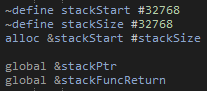
While, we have no dedicated hardware module for a stack pointer, it isn't too difficult to come up with an emulated stack pointer. This can be done by having a global variable in memory for the stack pointer itself. This pointer can go anywhere in memory, but will need to be set to some where the stack should be in memory when the program starts.
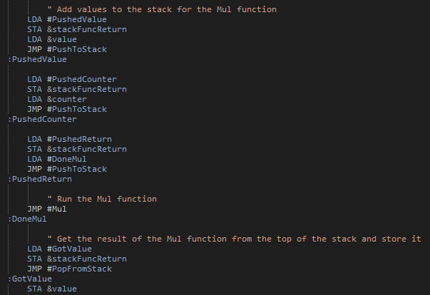
We next need to consider how the Push, Pop and Peek functions should be called. Clearly this can't be done in the same way that normal functions are done, as they will use the stack. So for this the general idea is that the function either puts or uses a value in register A, and then jumps the code back to where we where just running. I don't really think there is much use right now of having a dynamic method of getting the current instruction address as a piece of data, so instead we will just set another global variable to where we should jump back too using a label. This example then shows the rough way that a function is used. For each argument (and return location) the value is loaded into register A, the location to return from the stack function is set and then we jump to that stack function. We can then go to that function, which will need to pop the values from the stack, before putting the result back onto the stack. Finally we can pop that value and save it to memory.
With that in place we can start building more complex programs, making use of functions. For this first example I've defines a multiply function, taking two values from the stack, and putting the result back onto the stack. I think this should actually put the return location onto the stack before the arguments, so as to make calling multiple function calls easier. Anyway, with this function we can now do some more interesting tasks. For example, we can compute factorial numbers up to the maximum we can store (1, 2, 6, 24, 120, 720, 5040, 40320). It will be interesting to implement 32 or 64 bit numbers in the future to allow for larger values, although then we will also need a better method for displaying a number. It did take me a few attempts to get this program (Factorial.asm) working, but was extremely satisfying when it did:
I should note that to get the program working, I was making use of a simulated version of my computer which I should probably make a log on soon.
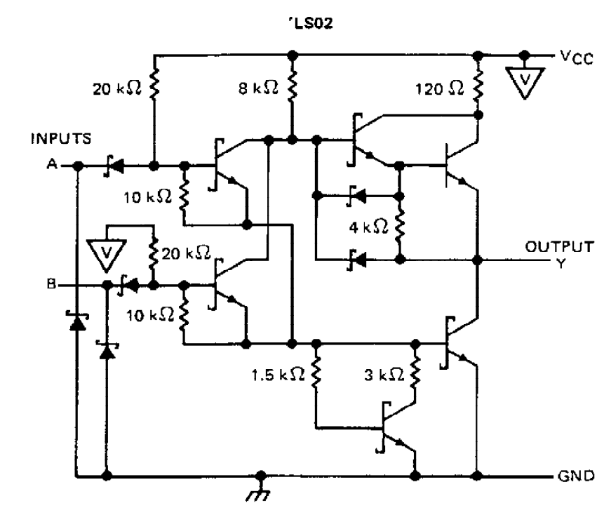
With this program running, I next considered a few improvements. The first one is that each of the stack functions can actually be performed in single instructions (although they do need most of the 16 micro instructions). This does work in my simulation, but unfortunately it isn't that simple for the physical thing. The issue is a bit complicated, but comes down to needing to decrement the stack pointer by one when popping a value from the stack. As there is no dedicated decrement by one function, we need to subtract one using the ALU. This has the issue of needing to load a value of one into register B, but without being able to pass a value as an OPERAND. A slightly bodged solution is to clear register X, and then increment it by one. This is unfortunately where the problem arises. The only way to clear a single register (as clearly resetting the whole computer isn't going to help) is to have the register load a value, while no value is being set on the bus. However, when trying this, the register will actually get set to have all bits high, rather than low. The data lines are all pulled low by a 1KΩ resistor, so this seems a little odd. However, I believe it is caused by internal pull up resistors in the 74LSxx ICs. I couldn't find anything for the actual register chips being used, but they should be similar to other ICs, for example looking at the 74LS02:
The inputs seem to have 20KΩ pullup resistors. So just considering this single gate (and ignoring the diode as I'm not quite sure what affect it has) this will create a potential divider, and so at 5V will put the undriven voltage at 0.2V. Which is lower than the maximum voltage for a logical low value (of about 0.8V). So while this doesn't seem to be a problem, if we consider that there are quite a few gates connected to these bus lines, its not so simple. There are actually about 10 modules that can read values from the bus, so actually the effective pull up resistance (again ignoring and diodes doing whatever they are doing) is about 2KΩ. So again with a 1KΩ pull down resistor, we will get about 1.7V on the bus when not driven (I seem to measure 1.44V). This is definitely above the maximum for a logic low, and so giving us the high bits. The most obvious solution is to use a smaller pull down resistor, say about 100Ω. This would again give us a voltage of 0.2V. However, this also increases the current from about 0.2mA to 2mA per data line (for a total increase of about 34mA). This probably isn't a huge loss, but the computer already uses a bit more current than I would like, so it isn't ideal.
New Modules
As much as I want the computer to be as simple as possible, there are several new modules that I would like to add. These should hopefully significantly increase the number of aspects of a real computer that I can implement, which is really the goal of this.
Clock
Currently the computer uses the clock designed for the original computer by Ben Eater. Which is on a breadboard, so clearly needs replacing. The clock I had designed doesn't really work, so I need to design something new. While I am at it, I should also redefine what the clock needs to be able to do.
- Manual mode
- Automatic mode
- Automatic mode frequency select
- Can be halted by the control logic
I already have a working manual mode (although I may need to adjust the debouncing) and the halting functionality. So its really just the automatic mode that needs fixing. There are two issues with the existing version. The signal generation needs to be improved, and there is no way to know what frequency is being used. It would also be nice to allow for a higher frequency, just to test how fast the computer can run. There is a fairly simple way that I can change this automatic clock. Rather than using a chip to generate the signal, it doesn't seem too much of a change to instead use an oscillator. This can be quite a high frequency, and then use binary counters to divide the frequency by some power of two. This not only gives a much cleaner clock signal, but also gives a much more accurate one with a known scaling factor, such that the final clock frequency is known. With a 4.1943MHz oscillator and 6 4-bit counters, I can pick a clock frequency all the way down to 0.25Hz. I could also use a lower frequency oscillator and fewer counter chips.
With this new automatic clock, there is one additional function I could now add: a timer. The oscillator will be running all the time, regardless of how the computer is running, what is more it is running at a known frequency. Also, to give the frequency scaling, I need to have counters anyway, so all I need to do is allow for the value stored in the counter chips to be put on the bus. The only issue with this is that a 16 bit value will overflow in 15ms with a 4.1943MHz oscillator. If I had a 32-bit value, it would overflow after 17 minutes. This still isn't a very long time, but much more reasonable and useful. This does however require 8 counter chips. I could reduce the frequency, but I am also quite interested in seeing the the computer can run with a MHz clock, so I would rather not do that. However, I can always start with a 4.19643MHz oscillator, and go to a slower one if I can't run it at that frequency anyway (or need a timer to last longer than 17 minutes). As oscillators have a standardised footprint, I should be able to switch between them fairly easily.
Stack Pointer Register
Rather than rely on a software stack implementation, I could make a dedicated register that can store the stack pointer. This would make stack instructions significantly faster. While I have said that speed isn't really a concern for me, when I have got the compiler functioning, the stack is going to be used a lot more. When this happens, it will likely become a major bottleneck in how fast anything can run, so it would be nice if it only took 3-5 clock cycles per instruction, rather than 15. Luckily, this new register is very simple to design. It is basically a counter register (the program counter and register X), but with a 74LS193 up/down counter.
SPI
This is the main module that was beyond the scope of the original plan. I had thought about some sort of graphical output from the computer, and while this is certainly possible, it requires some memory that needs to be continuously accessed to display the graphics to a screen, while also needing to allow for data to be read from the bus into that memory. I may still try this out in the future, but for now it either requires using chips beyond the limit of what I am willing to use in the computer, or a significant amount of custom logic to achieve this result.
So with a full graphics module out, what can I do instead. Well since starting this project I have done a lot more with microprocessors. These often make use of serial interfaces to communicate to other devices. One such is the interface is SPI. This can be made using shift registers, and so is definitely a feasible addition. What is more is that there are graphical displays that can use SPI, so I am still able to generate a graphical output. Alternatively, there are SPI general purpose input output (GPIO) chips that would allow for lots of other things to be connected up.
C Like Compiler
Since the previous update, I have mostly been working on the C like compiler. This is quite a big undertaking, so it is hardly surprising it is taking so long (I'm also in my masters year at university, so the time on projects is rather limited). There are several parts needed to make a compiler:
- Read source code
- Convert to tokens
- Valid and parse tokens into statements
- Generate assembly code
- Optimise assembly code (optional)
- Save output
However, each of these stages are actually quite complicated, and depending on how they are done, can become quite messy.
Read source code: Generally the simplest part, just requiring the contents of a text file to be read.
Convert to tokens: This is relatively simple, just requiring the input source code to be split up. This can be done by looking for whitespace, or other special characters (e.g. = + - ( ) ...). However, there is some added complication. Firstly, I wanted to allow for standard files (a bit like header files) that a program can include. This means that tokens from another file will need to be inserted in correctly, while also not including a file multiple times. Finally, I wanted to have compile time directives (e.g. #define X or #if X==0 ...). This adds a significant amount of complexity, not least due to needing to evaluate expressions at compile tine. Luckily, I made a system that can be used to do that in the past. This uses the shunting-yard algorithm as a means to convert an expression into reverse polish notation, which can then be evaluated using a stack.
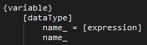
Valid and parse tokens into statements: This is possibly the most difficult part (although I haven't got to code generation yet), requiring some way to take an input stream of tokens, and work out what they mean. An obvious approach to this is to look at each token at a time and use a load of conditional logic to check what type of statement it is in. However, this required a fair amount of what I can only really describe as bodge. The issue is that every possible statement type needs to be hard coded into the system, which is viable for a small number of statements, but makes adding functionally increasingly more complex. An alternative approach is to use an abstract definition of what is a valid statement. This can be done using a tree structure. I also don't want to hard code this, so I needed to make another language to define this in a file. This needs to allow for generating an abstract tree like structure.
- {value} - Defines a statement type with the name given by the value
- [value] - Defines a pointer to another statement type with a name given by the value
- name_value - Defines a name type token with a given value
- numer_value - Defines a number type token with a given value
- string_value - Defines a string type token with a given value
Nodes are split up using a space with any other term being an operator token. When there are multiple child nodes they should be placed on new lines with the same indentation to indicate that the tree branches. For example if we want to add a statement to declare a variable we can use the following:
This defines a variable statement that needs the first token to be a valid data type (defined by some other statement). This can then either be followed by a name token with any value, or a name token with any value followed by the = operator, followed by some valid expression statement.
All we need to do now is match this abstract syntax definition with the tokens previously generated and we can not only confirm that the tokens are valid, but we can also build a list of statements along with the tokens associated with them. This still requires a certain amount of hard coding for each statement, but much less than previously, while also separating each statement type.
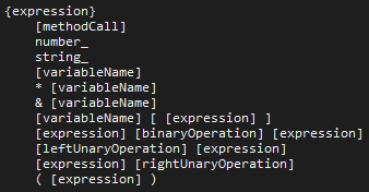
This is the current part I am working on. I have this working for simple statement, but have had some difficulty with nested expressions. For example I can define something like a = x + 3, but a = ((x + 3) * 4) + y has problems. This comes from how nested expressions get defined:
To match the abstract syntax definition with actual tokens is somewhat complex. The method I am using is similar to a pathfinding algorithm. However, the algorithm can easily waste time looking down incorrect infinitely long paths. Consider an expression followed by a binary operator followed by an expression, no tokens are required, so the algorithm can continue looking down an endless chain of these expressions. This could be valid to some level (e.g. a + 1 + 2 + 3 + 4 + 5 + 6 + 7 + 8 + 9...), in general it wastes a lot of time looking down the wrong path. What actually more problematic (and why I haven't got to the next stage of the compiler) is that a branching token needs to be able to check tokens after it, for example ( [expression] ). After the expression finds a valid match, the algorithm needs to also check that there is the operator ). This gets a bit difficult, and currently needs some fixing for complex expressions.
Generate assembly code: Here we need to convert the statements into assembly code. For some things, like variable definitions this should be quite simple. Even statements should be simpler here, using a similar system to how compile time directive expressions where handled. However, things like conditions and structs are likely to get somewhat complex.
Optimise assembly code: This step isn't strictly needed. The code generation stage should produce a valid program. However, to simplify how code is generated, there will be many inefficiencies. For example a value may not need to be stored to memory if it is going to be loaded back in to register A and then never used again, thus some instructions could be removed allowing for the final program to run faster. As the goal of computer isn't to run programs quickly, this stage is likely not going to implemented in full. There are many ways to optimise a program, and while some of them are fairly simple, many are not. It is also very easy to break a program by incorrectly optimising it.
Save output: Finally the assembly code can be saved back to a file, ready to hand to the assembler to make machine code.
Hopefully I can get at least a partially functioning compiler running soon. I specifically want to play around with structs, to see if I can implement larger data types such as a 32 bit or 64 bit integer. The current computer isn't able to display such a thing, but hopefully with the new modules I can make something interesting.
That's it for now. I still need to to a log about the simulation for the computer. However, I would like to make something that you can play around with, so will wait till I find time to work on that.
-
It Actually Works (Mostly)
09/22/2020 at 02:02 • 0 commentsThis project has been was sort of put on hold again shortly after the last log. While at the time I had made significant progress to getting it working (it could run most unconditional instructions), it promptly stopped working again. I also had only been working on it while I was unable to work on another project as I was waiting on something to arrive, so when I could continue with that this was put back on hold. However, as I decided to take a short break with that other project I decided to have another look at this one.
Additionally thank you for the comments, and sorry for not replying till now. Firstly for the clock I will probably use a Schmitt trigger to buffer the signal, but currently I don't have any so will stick to the 555 timer which does the job for now. Secondly, I'm not sure if there is a race condition, control bits should be set out of phase with the clock being active. But even after the fixes I will talk about shortly, I very much still need to use capacitors on the control lines to slow the signals down. Possibly the GLS29EE010 EEPROMS can't drive chips that far away in addition to an LED, and need a buffered output (dimming the LED may also help, and probably should be done anyway). For all data LEDs in modules, they are actually buffered using 74LS245 octal bus transceivers, so while it probably doesn't affect the ability for data to be moved around, it does result in quite a large current draw (especially when lots of modules have data). Finally, yes simple probably isn't the best term to use. But in comparison with even fairly simple microcontrollers or existing CPUs, it is relatively simple. At the very least I can built it and not worry too much about some aspects of the design.
So lets start looking at some of the problems the computer had. The first issue was that the output control bits for the current instruction register (CIR) where done incorrectly. This is mostly due to some unnecessary complication I added to allow for some extra functionality which is probably not going to be used. The CIR is a two word register where the 6 least significant bits give the OPCODE of the current instruction, while the remaining 26 bits give the OPERAND. This is needed because with only a single word, only a 10 bit OPERAND would be available and so only 1K words over RAM. Because I wanted the full 64K words available I need to allow instructions to make use of two words when the OPERAND is a memory address. This mean I need to be able to output a 16 bit value to the bus. However, if the OPERAND is a number less than 1024, then only a single word is needed and I only need to output a 10 bit value to the bus. Finally the overcomplication: With 26 bits of OPERAND available, I can allow for instructions to use two 13 bit arguments as an OPERAND. This lets me make full use of the two word CIR, but does mean that I need to allow for two 13 bit values to be outputted to the bus, one offset by an additional 13 bits. This gives 4 total output modes:
- FAST: The last 10 bits, from the first word
- FULL: The last 10 bits from the first word and the fist 6 bits from the second word
- MLT_0: The last 10 bits from the first word and the first 3 bits from the second word
- MLT_1: The last 13 bits from the second word
However, having multiple arguments isn't all that helpful (especially with a quite limiting 6 bit OPCODE, I should have made it 8 bits). The issue is that somewhere along the line the control logic for getting these different outputs got messed up. Firstly the FAST, FULL and MLT_0 control bits where being inverted, and secondly they where not being combined correctly anyway. Luckily, I could correct the problem quite easily by replacing an 74LS32 quad OR gate with a 74LS02 quad NOR gate, and redoing a few traces:
![]()
I also needed to un-invert the control bits. This is also quite easy, as each control word allows contains not only a GLS29EE010 EEPROM, but also a 74LS04 hex inverter. This doesn't allow for all control bits to be inverted, but as this is not needed for most bits this isn't a problem. To allow each control byte to be identical in hardware, each byte gives an inverted and non-inverted version of each bit, and so the connection can be easily swapped.
The next issue wasn't really that important, but it annoyed me enough for me to fix it. The issue was that because I made the first 32 words of RAM to be given in EEPROM, I needed to make sure that the RAM ICs and EEPROM ICs didn't try to output a value at the same time. However I always need one of them to output to make sure that the LEDs would show the value at the address given by the memory address register (MAR). What's more the RAM ICs being used (AS6C1008-55PCN) only have one data connection, meaning that the same pins are used for the data when reading and writing, making the control logic even more complicated. The result of all this added complexity is that I messed up a tiny bit and so the LEDs would only be lit if the RAM is currently reading or writing data, but not if neither operation was being performed. As I said this doesn't affect the functionality of the computer, but It does affect the lots of LEDs condition so needed fixing. Luckily it was an even easier fix than the last one, requiring only a few traces to be swapped around:
![]()
The previous problems where actually fixed around the time of the last log. However, even with these fixes, the full computer still didn't work. As a hopefully easier problem to solve, I decided to look at why one of my GLS29EE010 EEPROMS was always outputting high on all bits. This was actually on an unused control byte, but it still was something that needed fixing. The strange thing about this issue, was that my EEPROM programmer seemed to be able to write data to the EEPROM, and also read it back correctly. And yet the data would always seem to be high. Now, it is important to note that the programmer I'm using is designed by me, and so not immune to problems (in fact it has had quite a few since I built it). So to test where the problem is, I setup the EEPROM in a breadboard such that I could change the address and see what value was stored. This promptly showed that the programmer was correctly reporting that the data was all 0xFF (all bits high) where I had been looking. However, only in the first half of ROM. The second half had the data I had been expecting to be in the first half. This quite clearly points out the issue. The GLS29EE010 EEPROMS have 128KB of data, and so 17 address lines. However, in my programmer I use two 74HC595 8 bit shift registers to output the desired address from an Arduino Nano. To allow for programming all data, the final 17 address line is given directly. In this case the pin A5, typically an analogue pin on the Nano, but can also be used as a digital pin. However, in my code I accidentally used:#define ADDRESS_16 5
Rather than:
#define ADDRESS_16 A5So the address line was never being set, and so it seems was always being treated as high and so any data was being written to the wrong half of ROM.
This actually fixed quite a bit more than what I thought it would. At some point I also found a problem with the microcode of some instructions. While this had been fixed (or so I thought), and the EEPROMs reprogrammed. Due to the programmer having this issue, I had never applied the change.
The final fix is unfortunately not quite so described (and a problem I was rather dreading). With such a large project, it is quite likely that there are some poor solder joints somewhere. The problem with this, is that there are quite a lot of places this could be. Additionally, the joints will typically pass a continuity test most of the time. I really didn't want to check every solder joint everywhere, however I luckily had some hints that the problem was around the control logic. While I'm still not entirely happy that there aren't similar issues elsewhere, I did find a few places that definitely needed re-soldering (and removing some fluff), and low and behold:
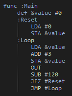
It actually works! The test program shown counts from 0 to 120 in multiples of 3, then resets. This is quite a good test as it makes used of addition, subtraction in the ALU; the A, B and OUT registers; as well as conditional and unconditional jumps. There are still a few parts that need to be tested, but we will get to that
So the computer works. This is quite good for my motivation so hopefully I will able to do some more with it shortly. There are still a few parts that aren't quite finished:
Clock
This is currently on a breadboard. Clearly not something allowed by my rules. It would sill be nice to use the original clock, but as mentioned at the start, I will need to look into using Schmitt triggers to buffer the signal. I may also look into having a high frequency mode using a crystal of some sort. However, I'm not really sure what the maximum frequency I can get with the computer. I think there is an absolute maximum of about 4MHz, due to the switching characteristics of the chips being used. But as I approach this frequency, I will also need to be careful about propagation delay to make sure signals don't arrive in the wrong order.
Program Memory
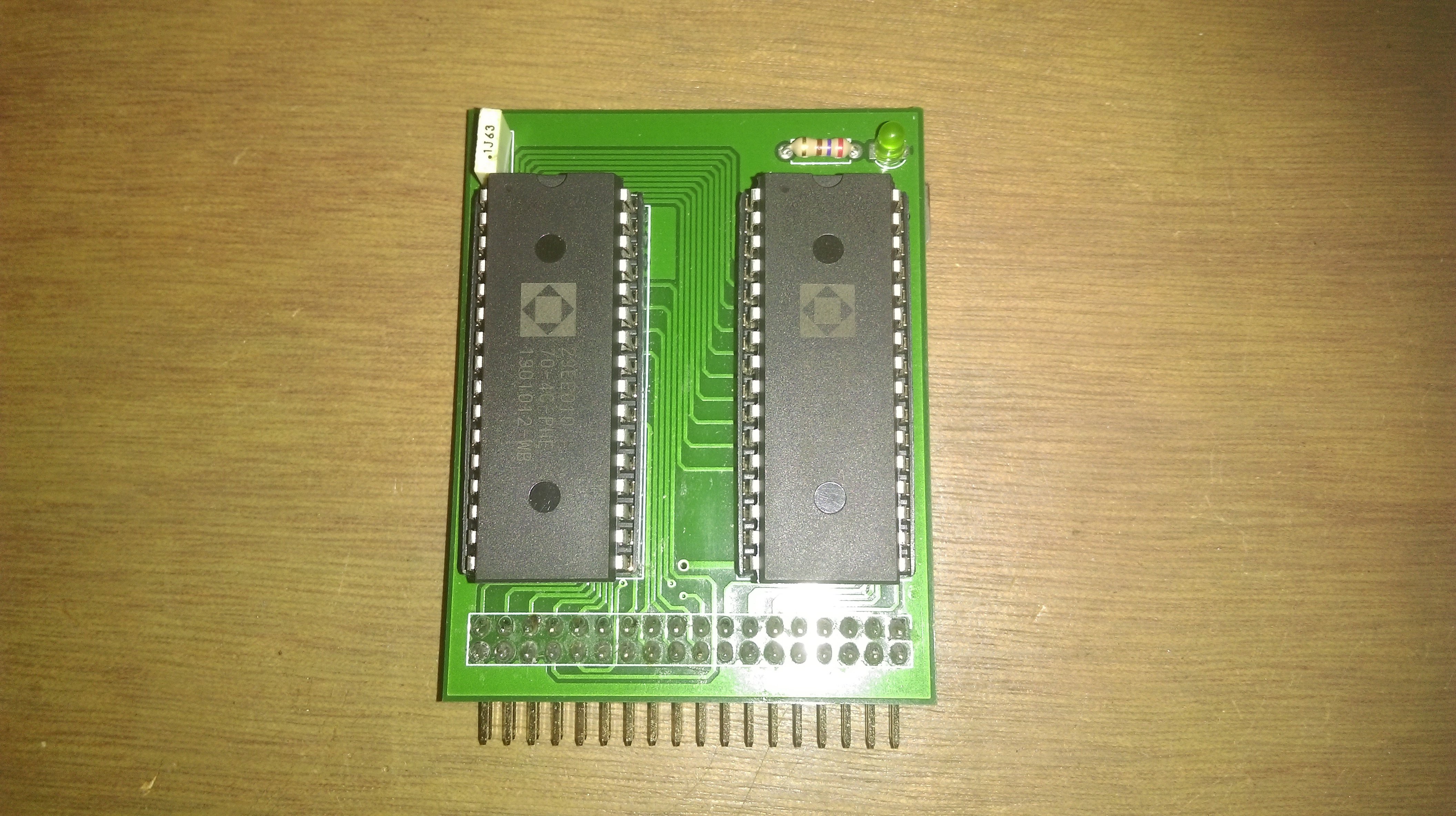
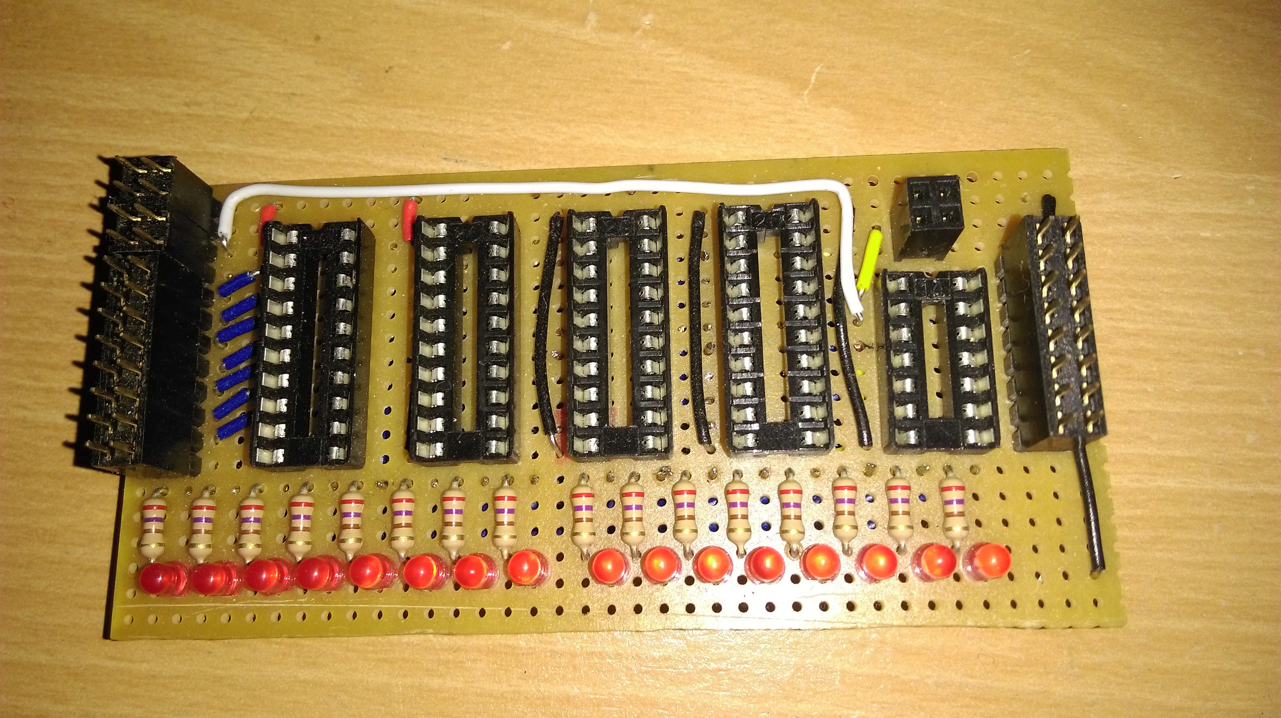
This is one of the main changes (other than using a 16 bit word obviously). While currently untested, I see no reason as to why these shouldn't work. Most of the hardware is duplicated from other parts, which seem to already work. However, my EEPROM programmer has had yet more problems. To store the program, I am using what I will refer to as a program card or program cartridge:
![]()
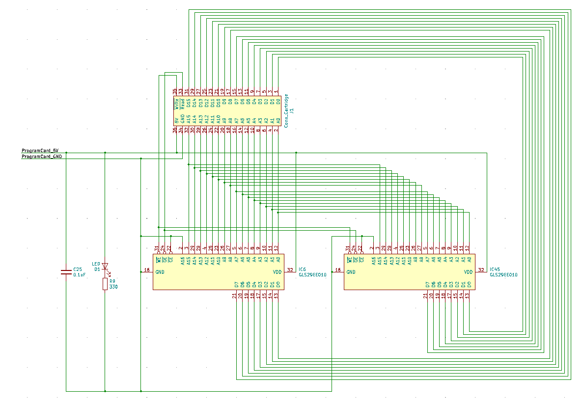
This consists of two GLS29EE010 EEPROMs, to make up a 16 bit word. Now in the design for this I have included the write and read enable controls in the connector. This means I can just plug this into my programmer board, and program both chips without removing them from their sockets (which risks damaging them). However, my programmer can only output a single byte at a time. Now if we look at the schematic of the program card:
If we consider what will happen during a write process it will quickly become apparent that when we write to one EEPROM, the other will also be in a write mode. But because we are only supplying the data to one of them, the other will have floating inputs. Due to how you program these chips, it probably wouldn't mess up the data, as it will never enter a programming state. But it is still best not write single bytes in this way. Rather than design a whole new programmer, I can split the write enable signals. As of writing this, I can only write one byte this way. But hopefully this will be solved shortly.
Input Register
This would be quite nice to get working. It probably doesn't need much work, but as it isn't all that important I haven't got round to it yet.
C Style Compiler
As this computer is off my own design, there isn't and normal compiler which supports it. I have actually already got an assembler which can be used to one to one convert instructions to the machine code needed to be put in memory. This also handles placing variables into RAM, along with allowing for blocks of code to eventually form functions. On that note, the computer does support functions, however there is no hardware module for a stack pointer. As such, implementing adding and removing items to and from the stack is quite slow (not that anything here is particularly fast anyway). However, implementing this sort of thing is quite a lot of hard work, really we want something to do that for us (and yes that means I'm using my computer with a GHz clock speed to program something that is currently less than 1KHz, but I would rather not spend all my time manually generating machine code).
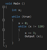
Let us consider the test program shown previously. This counts from 0 to 120 in increments of 3 and then resets, so lets look at the assembly code:
What we really want is to define something like this (and yes I know its note quite the same as the condition is in a different place):
Now this looks about the same amount of code. But this is also a very simple case. If we where to start doing anything even slightly more complex (imagine multiplying two numbers when all you can do is add and subtract), it will become far cleaner to use this C style code. However, this is going to be quite a lot of work, so don't expect anything too soon.
So there we go, the computer works for the most part. There are still a few things to sort out, but hopefully I won't run into my previous problem of not seeing any clear way to progress as I did before. I also would like to share one of my personal beliefs about this sort of thing. Every problem as a certain amount of time which you need to spend to solve it, the only reason you have yet to solve it is that you haven't spend the time working on it. Now maybe this isn't very good advice, but it helps me come back to something that has been left for a while, just in case I only needed a little more time to get it working. Although, it also seems that sometimes the best thing to do is leave a project for a short time. It can also be quite common that I suddenly have an idea about a solution to something even when not currently working on it.
Anyway, that will do for now. As usual, feel free to ask any questions. Hopefully I will get round to answering them slightly sooner this time.
-
Build Summery
08/15/2020 at 01:56 • 0 commentsAgain this will just be a summery of the build of the computer, to get mostly up to date with the project. Mostly of the actual work was done a little over a year ago, and unfortunately I didn't take as many pictures as I should have done at the time.
Build MethodThe first decision was exactly how to build all the modules. Clearly PCBs are a really good option (and the one I used) but there are still choices over how to have them made. However, originally I planned on using strip-board. This seemed a reasonable upgrade over breadboards, and so I started experimenting with building a register. That resulted in this:
![]()
While this looks rather promising and allows for fixes and modifications when needed, there is the slight problem of the other side:![]() This is clearly a mess (and I'm surprised that I did so much of it before giving up). It was very tedious to build, prone to error, and extremely difficult to debug and fix. The main issue being that with 16 data lines (needing a connection from the bus connection to the flip-flops, from the flip flops to the LEDs, from the flip-flops to the bus driver, and finally from the bus driver to the bus connection), and the remaining signal and power wired: over 70 individual wires are needed, and this is one of the simpler modules. As such I gave up building the entire system in this way. There are still some parts I still decided to used strip-board. Most notably the bus as it is so large, and mostly just a lot of parallel strips (i.e. exactly what a strip-board is). As an alternative fabrication method I had an experiment with making my own PCBs. For this I tested an EEPROM programmer for the AT28C16 ICs. For this I set up a headed container of Sodium Persulfate (as its apparently cleaner and more controllable than ferric chloride) with an air bubbler. To place a mask for the copper to keep, I experimented with laser printing onto paper, placing the paper toner side down onto copper clad board, heating the lot with an iron, and then removing the paper after soaking it in water for some time (there are definitely better tutorials out there that explain this). After a couple of attempts at transferring the mask I ended up with one I was happy with, etched and added the components:
This is clearly a mess (and I'm surprised that I did so much of it before giving up). It was very tedious to build, prone to error, and extremely difficult to debug and fix. The main issue being that with 16 data lines (needing a connection from the bus connection to the flip-flops, from the flip flops to the LEDs, from the flip-flops to the bus driver, and finally from the bus driver to the bus connection), and the remaining signal and power wired: over 70 individual wires are needed, and this is one of the simpler modules. As such I gave up building the entire system in this way. There are still some parts I still decided to used strip-board. Most notably the bus as it is so large, and mostly just a lot of parallel strips (i.e. exactly what a strip-board is). As an alternative fabrication method I had an experiment with making my own PCBs. For this I tested an EEPROM programmer for the AT28C16 ICs. For this I set up a headed container of Sodium Persulfate (as its apparently cleaner and more controllable than ferric chloride) with an air bubbler. To place a mask for the copper to keep, I experimented with laser printing onto paper, placing the paper toner side down onto copper clad board, heating the lot with an iron, and then removing the paper after soaking it in water for some time (there are definitely better tutorials out there that explain this). After a couple of attempts at transferring the mask I ended up with one I was happy with, etched and added the components:![]() This needed a few extra wires as it is a single sided board (double sided like this sounds difficult), but this needs far fewer than on the strip-board. The other side:
This needed a few extra wires as it is a single sided board (double sided like this sounds difficult), but this needs far fewer than on the strip-board. The other side:![]() Amazingly this worked with only a few traces needing to be fixed (some extra solder on traces at the top of the picture). There were a few issues with the process of making this. Firstly transferring the mask wasn't very reliable, perhaps I need to consider printing on thinner paper to stop the toner being pulled off when the paper is removed. Secondly, etching was rather inconsistent with the bubbler I used. The bubbler only really did anything directly above it, this can probably be fixed by using one that bubbles in a line, rather than from a point. Finally, and most importantly, the board stopped working shortly after it was made. This is likely due to damage to one of the traces from the lack of solder mask. Overall the process was somewhat successful, but probably a bit too unpredictable for what I want. What's more, I then discovered JLCPCB as an extremely cheap way to get two layer boards manufactured properly. I even got free 3ish day shipping with a test order I made (so I spent an entire £1.53 to get 5 test register PCBs). These tests looked very good, and let me use two layer PCBs so I ordered a full set of boards (unfortunately I had to pay shipping this time) along with all the ICs I expected I should need.
Amazingly this worked with only a few traces needing to be fixed (some extra solder on traces at the top of the picture). There were a few issues with the process of making this. Firstly transferring the mask wasn't very reliable, perhaps I need to consider printing on thinner paper to stop the toner being pulled off when the paper is removed. Secondly, etching was rather inconsistent with the bubbler I used. The bubbler only really did anything directly above it, this can probably be fixed by using one that bubbles in a line, rather than from a point. Finally, and most importantly, the board stopped working shortly after it was made. This is likely due to damage to one of the traces from the lack of solder mask. Overall the process was somewhat successful, but probably a bit too unpredictable for what I want. What's more, I then discovered JLCPCB as an extremely cheap way to get two layer boards manufactured properly. I even got free 3ish day shipping with a test order I made (so I spent an entire £1.53 to get 5 test register PCBs). These tests looked very good, and let me use two layer PCBs so I ordered a full set of boards (unfortunately I had to pay shipping this time) along with all the ICs I expected I should need. Modules
To build the computer I started with a roughly 560mm x 560mm x 6mm sheet of MDF. I then sketched out in pencil some construction lines before adding mounting points which the PCBs can clip onto. These have an M3 bolt going through the MDF into the post , so require some fairly well placed holes, based on each PCB. To make sure they where all lined up, I could hold each PCB over the correct place and make a pencil mark for where to drill holes. Overall I am very happy with this method of holding everything together, although maybe I should have used mounting posts where screw help the PCBs in rather than clips, so that they are easier to remove. Also I might paint the MDF at some point, but for now I will wait to everything is working. Soldering everything together was pretty simple (although the LEDs and their resistors took a while). I also tried to test all the modules separately as thoroughly as possible before putting it all together. This got me to this state:
![]() Finally, I needed to wire it all together. To make things look vaguely nice, my plan was to solder small pieces of strip-board onto header pins to make a more easily solderable connector, and then use solid core wire to connect them together:
Finally, I needed to wire it all together. To make things look vaguely nice, my plan was to solder small pieces of strip-board onto header pins to make a more easily solderable connector, and then use solid core wire to connect them together:![]() After quite a bit of tedious soldering I am very happy with the "finished" look. As a colour code, red is 5V, black is ground, white is clock, yellow is signal and blue is either data or an address (maybe I should have made addresses a different colour, but I'm not redoing these if I don't have to). For the yellow signal lines, I added some electrical tape to hold things together so they look nice (might might have been a bad idea due to interference, but it looked better than everything allover the place). There is also sort of a colour code the the LEDs: red is a data (which is sometimes an address) value in a module, blue is control (either the OPCODE or control word) and yellow is somewhat variable; being the micro-code counter in the control logic, the OPERAND in the IR, and the current value on the bus.
After quite a bit of tedious soldering I am very happy with the "finished" look. As a colour code, red is 5V, black is ground, white is clock, yellow is signal and blue is either data or an address (maybe I should have made addresses a different colour, but I'm not redoing these if I don't have to). For the yellow signal lines, I added some electrical tape to hold things together so they look nice (might might have been a bad idea due to interference, but it looked better than everything allover the place). There is also sort of a colour code the the LEDs: red is a data (which is sometimes an address) value in a module, blue is control (either the OPCODE or control word) and yellow is somewhat variable; being the micro-code counter in the control logic, the OPERAND in the IR, and the current value on the bus.
This was then the point where I thought it would be done, maybe some work fixing small issues, and then I could consider additional modules for it such as some sort of graphical output. However, things are never quite that simple. Upon powering it up (using a 5V 3A phone fast charger) it was very clear there was some more than small issues with the computer. This was mostly characterized by the values in modules updating randomly, and not synchronized with the clock. The control logic was also able to output values not valid based on how they had been programmed (outputting 0xFF which was only programmed to parts of memory which had address lines pulled to ground so couldn't be accessed).
Having run into these problems, I got rather fed-up with the whole project as I don't have a digital oscilloscope, and my logic analyzer isn't fast enough to see any issues. However, after spending some tome working on other projects (mostly model rockets) I eventually came across this video on Schmitt triggers on the EEVblog. The most relevant part of this, is that it introduced me to the issues when a signal takes too long to change from low to high or vice-versa. Looking at the datasheet for CD4047BC (which is used to generate the clock signal), the rise and fall time at 5V has a maximum if 15μs. I haven't been able to find a maxim rise or fall time for any 74LSxx ICs, some 74HCxx chips give the value at about 500ns at 5V. What is more, some 74LSxx datasheets give the rise and fall time in test conditions, with the values being all less than 10ns. While this isn't going to be anywhere near the maximum time, it does give us a rough target of what we should be using. So clearly having a clock with a rise time up to 3 orders of magnitude larger than the typical value is a problem. Having looked at this I decided to test using an Arduino Nano as a more controllable clock (which needed the clock to be buffered as it couldn't drive everything) and soon found that while the computer still didn't work, there was a significant improvement in the overall stability of everything. For the time being I have gone back to the clock used in Ben Eater's original computer. This still isn't perfect, but has definitely improved things so will have to do for the time being.
In a second attempt to revive the project I upgraded the power supply. The old one was a 5V 3A phone fast charger, and while this was able to maintain the voltage at just below 5V, from testing with lower current supplies (which definitely couldn't maintain anything like 5V), I decided that keeping a consistent supply at higher voltages might be a bit much for the power supply. As a replacement, I got a proper 5V 10A supply of the sort often used for higher power hobby electronics. This uses a screw terminal to connect a main power cable, and had absolutely no cover over this terminal. As such, I 3D printed a cover and resulted in a very nice, and capable, 5V bench power supply for anything that needs it. However, I'm not convinced it really did much to help the computer, and I don't really have anything to measure how smooth the power supply really is.
That more or less catches up with where I was before properly reviving the project. In the next log I will talk about some of the fixes I have made (which have made me realize it is possible to get this working), as well as answer any questions anyone has about anything a bit more specific than I have so far gone into. -
Initial Design Summary
08/10/2020 at 00:22 • 0 commentsBecause this project has been going for a while (started about 20 months ago as of writing this), I will make a summary of the progress made up to to when I created the project here.
The general idea of the computer is the same as the one designed by Ben Eater. However, I want to make a computer which firstly I have designed, and secondly is capable of running something interesting. As such, the general design will be the same. However, the computer will be 16-bit and have some redesigned modules.
Before this project I had done some electronics projects, but basically only for GSCE electronic at school. This was my first large scale unguided project, and also my first with properly build PCBs. So take that as a warning that there are going to be some stupid choices made in the design.
DESIGN
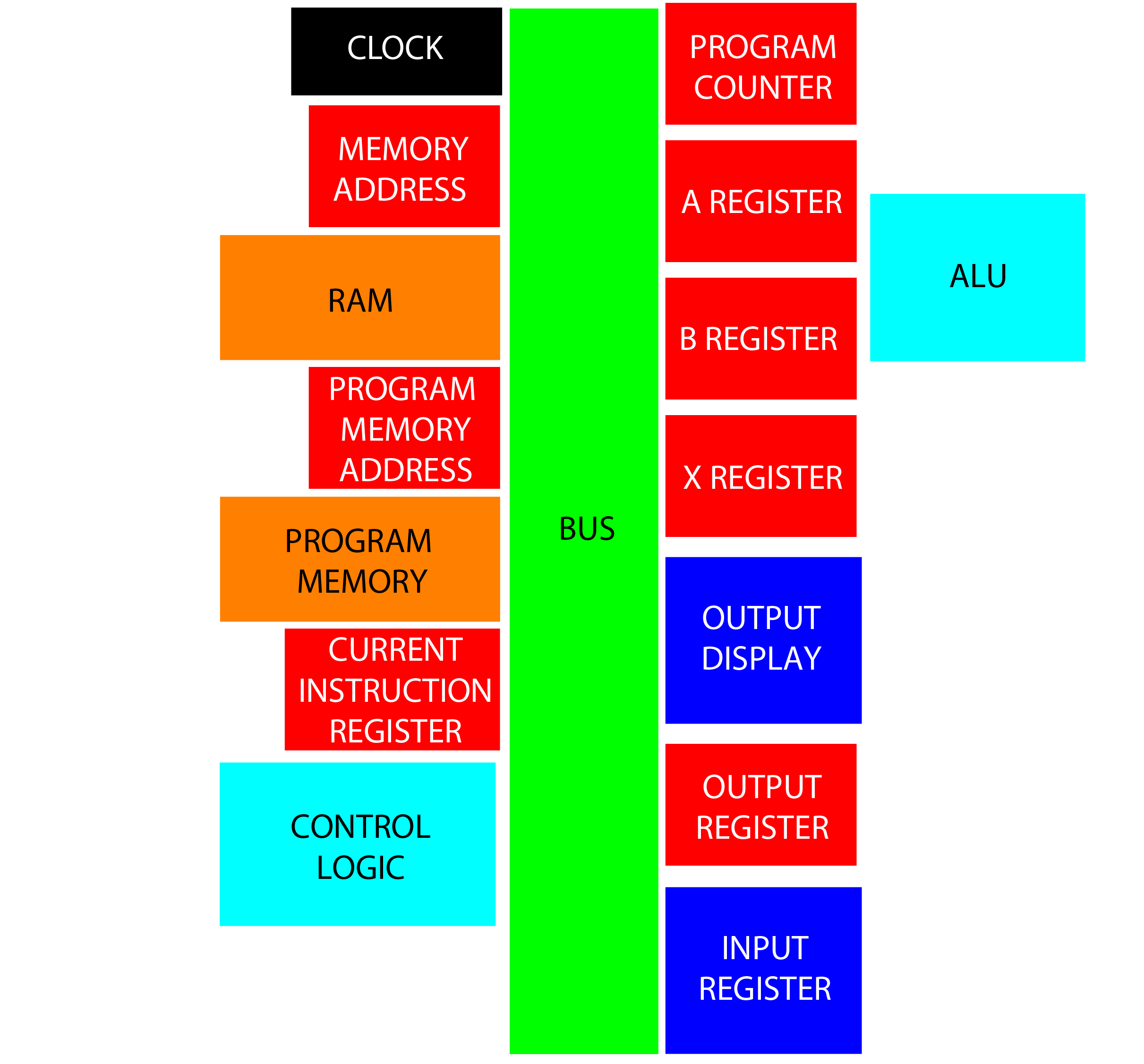
Firstly, I needed to pick the modules to include in the initial design of the computer (with the idea that mode would be added later). Clearly there are some that are required for the computer to function which I will call core modules while others add additional abilities to the computer which I will call function modules. Also all modules should have LEDs to display the value currently stored in the module.
CORE:
- Clock
- Synchronizes the computer so everything will work correctly
- Program counter (PC)
- Stores the memory address of the next instruction to read
- Memory Address Register (MAR)
- Stores the memory address which the RAM either read or write to
- Random Access Memory (RAM)
- Stores all the working data and instructions (instructions could be read from some other memory)
- Current Instruction Register (IR)
- Stores the data for the current instruction being run
- Made of an 6-bit OPCODE and OPERAND
- To allow access to all of RAM, this needs 6 bits for the OPCODE and 16-bits for the OPERAND. As such this can be a 2 word register.
- With 26 bits for the OPERAND we can have several modes of outputting the OPERAND to the bus
- FAST: 10-bit OPERAND so only the first word needs data make the operation faster to execute
- FULL: 16-bit OPERAND so all of memory is accessible, but both words need data
- MLT_0: First of two 13-bit OPERANDS allowing for two arguments to an instruction
- MIL_1: Second of two 13-bit OPERANDS allowing for two arguments to an instruction
- Control Logic
- Decodes the OPCODE and any flags to a control word used to control all parts of the computer
FUNCTION:
- Arithmetic Logic Unit (ALU)
- Performs all mathematical and logical operations using values in the A and B register
- Initially this is limited to addition and subtraction
- A Register
- Stores the value currently being worked on by the ALU
- B Register
- Stores a modifier value which the ALU uses to act on register A
- X Register
- Index register, used to store a pointer to a value in an array
- Needs to be able to increment by 1 without using the ALU
- Output Register
- Stores a value to be displayed in some way
- Should also have a decimal decoder of the value stored
- Input Register
- Used to store a user input
- Program Memory Address Register (PMAR)
- Stores an address in program memory for an instruction or constant to fetch
- Program Memory
- EEPROM storage of write only data to store instructions and constant for a program
- The actual storage should be easily removable such that the program being run can be changed easily
These will all be connected with a central bus, and can have the following rough layout:![]()
While I could go into the design of each of these modules, this would end up being rather long. So I will summarize the main parts. Firstly a number of the modules are functionally identical, so can use the same base module, possibly with some small changes. So the A and B registers use the same hardware, while the output register is also the same, but does not need the components to output to the bus to be populated. Similarly PC and X have the same hardware, as do MAR and PMAR. The IR can also use the same parts as MAR, but will need to modules to get a 32-bit word, and also need a module to allow for each output mode to the bus. Here are a rough design to the main modules.
Clock:
This uses a CD4047BC low power multivibrator. This uses only a single resitor and single capacitor to control the frequency. As such, it is simple to produce a 50% duty cycle square wave at a large range of frequencies (unlike on a 555 timer). As such, some dip switches can be used to change which resistor and which capacitor are being used, along with a variable resitor for finer tuning of the frequency. The rest of the module is roughly the same as the Ben Eater clock.
Simple Register:
Uses two 74LS273 octal flip-flops to store data, needing an extra 74LS08 AND gate to combine the read data and clock signal. Also uses two 74LS245 octal bus transceivers to output data to the bus. This allows for the module to output the data stored in the flip-flops to be displayed with LEDs, while also allowing for conditional output to the bus. This output method is common to all devices capable of driving a value onto the bus.
Index Register:
Uses the same output method as the simple register, but has four 74LS161 4-bit counters to store the data and allow for the current value to be incremented by one.
Address Input:
This is the data storage part of the simple register, but with no bus output. Instead there is a 16-bit connector for sending the data to some other module.
ALU:
This is rather complicated module, even for just addition and subtraction (which is why no other operations are available), using 14 total ICs. The main ones being four 74LS283 4-bit full adders to perform the operation as well as the same ICs as the simple register to output to the bus. The module also needs to produce signals for when the operation resulted in zero or when the carry bit of the final adder is set. This means that two 74LS02 NOR gates and two 74LS08 AND gates are needed to check if any bit is non zero. There also needs to be four 74LS86 XOR gates for conditional inverting of the B register for subtraction.
RAM:
Yet another complicated module. For the actual storage I am using a pair of AS6C1008 128k x 8-bit low power CMOS SRAM. This particular chip is compatible with the TTL logic of the 74LSxx series chips used everywhere else. However, they use the same pins for data input and output, and so while the same ICs are used as before for the output, they need additional controls for which data is allowed to pass in. I also decided to over complicate things by having a built in read only memory (ROM) to store so initial program to run. The idea with this was to have a some instructions to copy the program from the program memory to RAM, before running the program exclusively from RAM. While this will work, my more recent dealings with microprocessors has made me realize that it might just be easier to only allow instructions to be stored in program memory, and they are copied from there to the IR rather than needing to have all the instructions copied to RAM before the program can execute. However, the design has the ROM, which then needs control over when to output a value from ROM, rather than RAM. For this I am allowing either 16 or 32 words of ROM (4 or 5 bits). This means that if all higher bits are zero, then ROM is enabled rather than RAM. This makes use of a rather complicated layout of two 74LS02 NOR gates, two 74LS08 AND gates and a 74LS04 NOT gate. The clock signal is also decoupled from the rest of the computer using a serial pair of NOT gates followed by a edge trigger using a 1k resister and 10nF capacitor, which I found an explanation for here. The ROM chips don't need to be very large, and because I have already made use of them I am using the same AT28C16 2k x 8bit parallel EEPROMs used by Ben Eater for the original computer.
Program Memory:
This is mostly just the output from the simple register, with an address input. There is also a connector to an external storage cartridge. This and connections for 16-bit address, 16-bit data, power, read enabled and write enabled. The write enabled is available to make programming the cartridge easier, as the EEPROM chips do not need to be removed. For the choice of EEPROM, the AT28C16 used in the RAM do not have enough address bits for the full 16-bit address. While these aren't really needed, the address is available so I am using two GLS29EE010 128k x 8-bit page write EEPROMs. These have more than enough address bits, but unfortunately are a bit of a pain to program (I wont go into it know, but I might at a log about it at some point).
Output decimal decode:
This takes the value in the output register and uses two more GLS29EE010 EEPROMS with a 555 and 74LS76 dual JK flip-flop to scan over each of five 7-segment displays at a high enough rate that they all appear to be on. There is also a sixth 7-segment display that can display a negative sign if the most significant bit is set. This allows for a twos compliment signed value to be displayed. Unfortunately the EEPROMs don't have enough address lines for both signed and unsigned decoding to be stored, so they need to be reprogrammed to changed output mode (rather than just moving the jumper).
Input:
This is just the output part of a simple register, with connection to some external module to actually handle the user input. This other module can be changed depending on the what sort of input is required. This module also need to be given an indication that the control logic is requesting an input (and so the computer is halted), as well as a return signal for when an input is available (so the computer can resume).
Control Logic:
There are two main sections to this module. Firstly there is a micro-instruction register and flag register, made from a 74LS161 4-bit counter and 74LS173 4-bit register respectively. There is also a 74LS02 NOR gate to manage resetting the micro-instruction register and full system reset. The second part to the module is a series of control bytes. These are able to be chained together to form an arbitrarily long control word. Each of these bytes uses a GLS29EE010 EEPROM with an address of the OPCODE from the IR, current micro-instruction and the 4-bits from the flags register. As some of the control bits are active low, there also needs to be a 74LS04 hex inverter allowing for 6 of 8 bits of each control byte to be inverted if needed. This does mean that some thought needs to be given to the ordering of control bits, but most control bits are active high, so there is no point in adding and extra inverter for the final two bits.
That still took quite a while to explain, and doesn't cover all of the computer but hopefully it gives a rough idea of the parts of each module. The next part was PCB design. I will skip over this completely as it was done quite a while ago and wasn't done particularly well.
The next log will go over the build process so far, to catch up to where the project is as of the project being added to hackaday.io. - Clock
Simple 16-bit Computer
Simplified 16-bit computer using mostly 74LSxx logic
 This is clearly a mess (and I'm surprised that I did so much of it before giving up). It was very tedious to build, prone to error, and extremely difficult to debug and fix. The main issue being that with 16 data lines (needing a connection from the bus connection to the flip-flops, from the flip flops to the LEDs, from the flip-flops to the bus driver, and finally from the bus driver to the bus connection), and the remaining signal and power wired: over 70 individual wires are needed, and this is one of the simpler modules. As such I gave up building the entire system in this way. There are still some parts I still decided to used strip-board. Most notably the bus as it is so large, and mostly just a lot of parallel strips (i.e. exactly what a strip-board is). As an alternative fabrication method I had an experiment with making my own PCBs. For this I tested an EEPROM programmer for the AT28C16 ICs. For this I set up a headed container of Sodium Persulfate (as its apparently cleaner and more controllable than ferric chloride) with an air bubbler. To place a mask for the copper to keep, I experimented with laser printing onto paper, placing the paper toner side down onto copper clad board, heating the lot with an iron, and then removing the paper after soaking it in water for some time (there are definitely better tutorials out there that explain this). After a couple of attempts at transferring the mask I ended up with one I was happy with, etched and added the components:
 This needed a few extra wires as it is a single sided board (double sided like this sounds difficult), but this needs far fewer than on the strip-board. The other side:
 Amazingly this worked with only a few traces needing to be fixed (some extra solder on traces at the top of the picture). There were a few issues with the process of making this. Firstly transferring the mask wasn't very reliable, perhaps I need to consider printing on thinner paper to stop the toner being pulled off when the paper is removed. Secondly, etching was rather inconsistent with the bubbler I used. The bubbler only really did anything directly above it, this can probably be fixed by using one that bubbles in a line, rather than from a point. Finally, and most importantly, the board stopped working shortly after it was made. This is likely due to damage to one of the traces from the lack of solder mask. Overall the process was somewhat successful, but probably a bit too unpredictable for what I want. What's more, I then discovered
 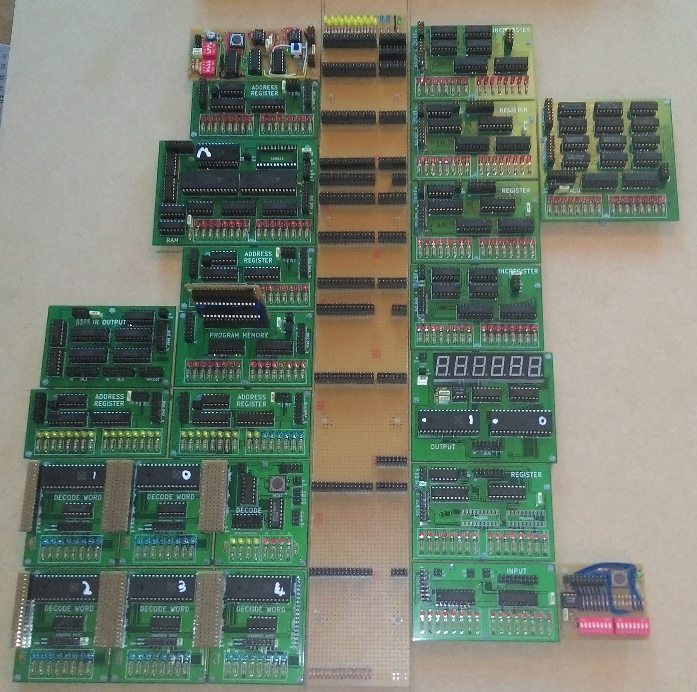 Finally, I needed to wire it all together. To make things look vaguely nice, my plan was to solder small pieces of strip-board onto header pins to make a more easily solderable connector, and then use solid core wire to connect them together:
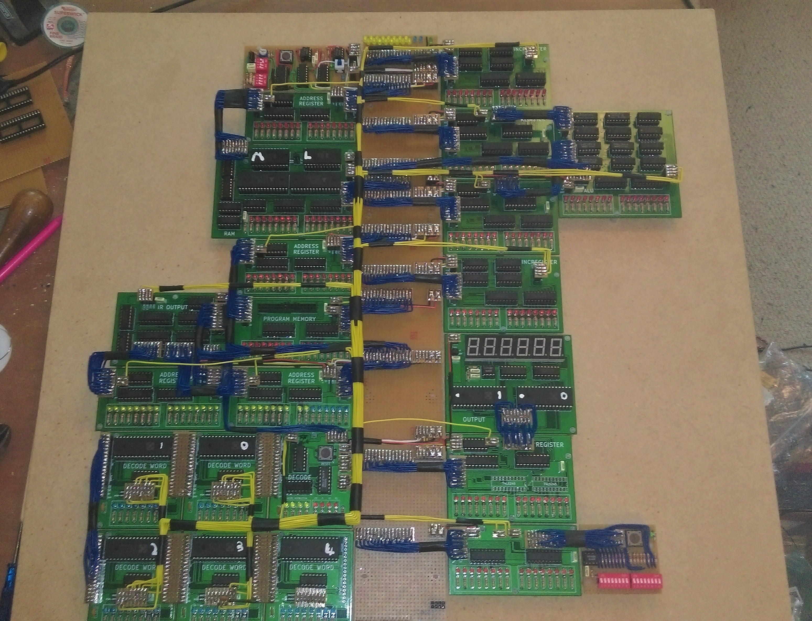 After quite a bit of tedious soldering I am very happy with the "finished" look. As a colour code, red is 5V, black is ground, white is clock, yellow is signal and blue is either data or an address (maybe I should have made addresses a different colour, but I'm not redoing these if I don't have to). For the yellow signal lines, I added some electrical tape to hold things together so they look nice (might might have been a bad idea due to interference, but it looked better than everything allover the place). There is also sort of a colour code the the LEDs: red is a data (which is sometimes an address) value in a module, blue is control (either the OPCODE or control word) and yellow is somewhat variable; being the micro-code counter in the control logic, the OPERAND in the IR, and the current value on the bus.