Close
0%
0%

100MHz TTL 6502

Experimental project to break the 100MHz “sound barrier” on a TTL CPU

Similar projects worth following
An often repeated refrain is that homebuilt CPUs are constrained to single-digit clock-rates by limitations inherent in discrete-component design. But we know that's not true. The C74-6502 (https://c74project.com/ ) achieved a 20MHz clock-rate while still being a full-fledged cycle-accurate 6502. It's worth asking, then, could a humble TTL 6502 reach that rarified air above 100MHz? It’s not clear such a thing is possible, but the challenge is on!

Team C74 is once again on hand and the objective is to build a next generation TTL 6502 with the highest clock-rate we can muster. The focus will be on reducing the cycle-time while keeping CPI fixed. The over-arching goal as always is to learn and to have fun. This project promises ample opportunity for both, so we'll buckle-up and get ready for a bumpy ride! 

The effort breaks down into a few key strategies:

1) Use faster hardware
2) Optimize critical circuits
3) Increase parallel processing
4) Manage signal integrity

Let's look briefly at each in turn.

Memory is a key area where faster hardware is essential. Both external memory and the microcode store will need to keep up with a faster clock-rate. Fortunately, access-time can be reduced almost at will using RAM. Hobby-friendly 10ns RAMs are readily available, and synch RAMs are even faster. The latter expect an addresses in advance of the cycle, and deliver in return access-times that are vanishingly small. It's safe to say memory is not likely to be a bottleneck in this design.

By the same token, there are also faster logic families available. The 3.3V LVC family, for example, has a good selection of parts at almost twice the speed of AC logic. The CBTLV family offers 3.3V variants of FET switches which can be very fast when deployed correctly. And then there is the AVC and AUC families. With near-nanosecond propagation delays, these families also feature variable impedance outputs which "provide great signal integrity without the need for external termination when driving traces of moderate length (less than 15 cm)". All-in-all, it's an embarrassment of riches when it comes to fast components.

But there are limitations also. For example, there is no equivalent to the 74AC283 Adder in these faster families, and FET switches are no faster with Select signals than their AC family cousins. Some careful design will be needed in critical circuits to capture the potential gains. ttlworks’ FET Switch Adder is a good example this, but there are others. The Decode, Flag Evaluation, and Branch Testing circuits are a few examples that are likely to land on the critical path.

Beyond specific optimizations, we'll need to look to increased concurrency. The C74-6502 divided its processing into two stages: the FETCH stage, and the everything-else-stage (aka EXECUTE). An obvious improvement is to split EXECUTE into shorter phases. As we discovered, pipelining can get very complicated very quickly, with multiple caches, hazard checks and branch prediction schemes. So we'll need to be careful lest the whole thing get out of hand. Thankfully, there are significant gains to be had with more TTL-friendly techniques. More on that later.

The final leg of the race is all about signal integrity. Trace geometry, stackup and clock management will all need careful attention. We are likely to need six layers boards, impedance controlled traces and a mixed-voltage supply. It's gonna be fun.

It was not until 1992 that DEC Alpha and HPPA RISC took the computer industry as whole beyond the 100MHz mark. Is it possible for a discrete-component 6502 to reach that same 100MHz milestone today? Well, we're gonna try to find out!

  • Pipeline (2)

    Drass11/12/2020 at 03:25 0 comments

    I wanted to touch on a final aspect of this pipeline design and the specific problems it helps to overcome. I struggled a bit with this explanation, so apologies in advance for any confusion. I’ll be happy to try to clarify so please just ask. Here it goes ...

    Unlike the atomic instructions we find in a traditional RISC pipeline, even basic operations in this design are spread over two microinstructions. For example, a typical RISC style add operation, like this:

    add r1, r2, r3

     takes two microinstructions to specify in this pipeline, corresponding to the 6502 FetchOperand and FetchOpcode bus cycles, like this:

    ALUin(A, DB, C); PC += 1                # FetchOperand
    A := ALUop(ADD); IR := DB; PC += 1      # FetchOpcode

     The first microinstruction loads the inputs of the ALU and the second performs the ALU operation itself. To be clear, the RISC form of the instruction would execute the same sequence of steps with respect to the ALU as it works down the pipeline. But it remains an atomic unit that describes only a single operation.


    By contrast, a single microinstruction in this design can specify the ALUop for one operation and the ALU inputs for the next. For example, during indexing, we might see the following microinstruction:

    ADL := ALUop(ADD); ALUin(ADH, 0, Cout)

     This microinstruction completes the sum for the low-byte of the address (ADL) and also sets up the ALU inputs to adjust the high-byte (ADH). Because of their dual-function, only one of these microinstructions is required to manage the activity across both the DECODE and EXECUTE stages.

    D72D8FF6-B463-4F19-8A4F-42F9AD9BCFA1.jpeg

    As a bonus, that one microinstruction can also specify whether any ALU outputs need to be recirculated (as is the case with Cout in the microinstruction above).

    Most importantly, though, the arrangement allows the pipeline to avoid control stalls. To see how, consider the effect of a FetchOpcode operation on the pipeline. A FetchOpcode causes microinstructions for a new opcode to begin to be fetched from a new location. In that sense, we can think of the opcode as an address and of FetchOpcode microinstructions as unconditional branches to opcode "subroutines". From the point of view of the microinstruction stream, a FetchOpcode is in fact an unconditional branch.


    0AF13418-5175-4786-9C77-AC7FA5652D4B.jpeg
    And just like all pipelined branches, FetchOpcode invalidates any instructions that have already been pre-fetched into the pipeline at the time it executes. This is effectively a "branch delay slot". With a traditional pipeline, there are two such invalid instructions, one in the FETCH stage and another in the DECODE stage. In this case we can use the opcode itself in place of the microinstruction in the FETCH stage. But the microinstruction in the DECODE stage has to be discarded. Left as is, the pipeline would stall.


    7F61A5E2-7825-4C8E-A82A-DAAF19009B02.jpeg
    This is where the "split" microinstructions come in handy. Since there is only one microinstruction active for both DECODE and EXECUTE, we can take the opcode and just keep going. No control stall is triggered and no extra cycles added to the processing as a result.

    Alright, with that final gremlin banished, here now is a high-level block diagram for this CPU.


    BDE32586-357C-494B-BDF1-F5C63F430764.png

  • Pipeline Overview

    Drass11/04/2020 at 23:03 0 comments

    Let's now take a closer look at the pipeline in this design. The objective is to reduce the cycle-time while keeping the cycle-count fixed. The critical path in the CPU falls squarely on the ALU, and associated pre- and post-processing. Rather than cramming all this into one cycle, the basic strategy is to push pre-processing to the prior cycle, and post-processing to the next. This allows the ALU to have the whole cycle to itself, giving us the headroom we need to boost the clock-rate.
    8EE48AA7-1063-4FE1-9FE5-2F36299202AF.jpeg
    Pre-processing here refers to the work required to set up the inputs to the ALU with appropriate values. That seemingly innocuous task takes a surprising amount of time -- we have to fetch microcode, decode control signals, select source values and output-enable the approriate registers. Post-processing, on the other hand, refers to updating the status flags and writing to the destination register. Rebalancing this workload around the ALU, we end up quite naturally with a four-stage pipeline, as follows:
    0A20172C-7EE4-4D9D-96DE-9DFC021A9BF8.jpeg
    We have FETCH, DECODE, EXECUTE and WRITEBACK -- the idea is to perform a roughly equal amount of work at each stage and then to pass the baton to the next. Along the way, we capture intermediate results in pipeline registers. Specifically, we have the Microinstruction Register (MIR) after the FETCH stage, we have ALUA, ALUB and ALUC registers at the ALU inputs and we have the R register at its output. The FTM (Flags To Modify) and RTM (Registers To Modify) registers direct the WRITEBACK stage regarding which flags and destination register to update. (More on the WRITEBACK stage below.)

    Memory operations using "flow-through" synch RAMs are a good fit for this arrangement. A key feature of these RAMs is that we can clock an address into the RAM's internal registers then read the data value from its outputs before the next clock edge occurs. The ADL and ADH registers allow the pipeline to work in this same way with asynchronous peripherals. For writes, there is also the WE register and a Data Output Register (DOR).
    D50672AF-FBC0-4152-8AC2-424CA09C1F35.jpeg
    As we've discussed before, the ALU features a "recirculate" path to allow the result to be fed back into its inputs. This is done during address calculation, for example, when the ALU result is immediately required in the next cycle. Memory reads are also recirculated, as either ALU operands or addresses to be used in the next cycle.
    E7B259A6-3F7B-478E-B5C7-D5FBF8A343C2.jpeg
    The WRITEBACK stage calculates the flags based on the ALU result, updates the P register according to the FTM, and writes the result to a destination register according to the RTM. 
    16FC68AD-EC89-4E0D-8C9C-6E79EC7FE30A.jpeg
    One important thing to highlight is that the WRITEBACK stage writes to registers using a mid-cycle rising clock-edge (PHI2 rising edge). Meanwhile, registers are always sampled at the end of the cycle (PHI1 rising edge). This discipline ensures that we always get an up to date value when a given register is being read and written to in the same cycle. For example, the P register may be updated in the same cycle that a branch test is being executed. Delaying the branch test until the second half of the cycle ensures that the branch test evaluates correctly.
    FE96582E-0EDA-4322-B47B-08E82FCF4BBC.jpeg
    Beyond allowing enough time to calculate the flags, a separate WRITEBACK stage allows the R register to neatly buffer the ALU from the rest of the CPU's internal registers (and the added bus capacitance they would impose). There are over ten destinations for the ALU output, all of which would add unnecessary delay to the ALU's critical path were they connected directly (10 loads x 3pF per load x 50Ω + 6" trace delay = 2.5ns). 

    Finally, we should note that the DECODE stage must receive a fresh instruction every cycle in order for the pipeline to function smoothly. To begin with, FETCH retrieves a new opcode from main memory (or simply generates a BRK on a CPU reset) and feeds it to DECODE stage via the Instruction Register (IR).
    7D710D00-CA4C-4635-A91A-B0BB487A09C9.jpeg
    Thereafter, FETCH will retrieve microinstructions associated with that opcode from the microcode store, one per cycle, and feed them to the DECODE...

    Read more »

  • Decimal Mode

    Drass10/26/2020 at 16:27 1 comment

    The basic method for Decimal Mode is to perform an ADD or SUB operation, and then convert the result to BCD. The process is to work on each nibble in turn, as follows:


    Adder LO --> Detect LO --> Generate LO --> Adjust LO --> BCD result LO
    Adder HI --> Detect HI --> Generate LO --> Adjust HI --> BCD Result HI

    Detect_LO tests to see if the lower nibble needs to be adjusted. This would be the case if the the binary result is greater than 9, or if the low-nibble carry (C4) is high. To adjust an ADD result, Generate_LO will generate a 6 (or 0 if no adjustment is needed) which is then applied to the binary result by Adjust_LO. Generate_LO will also generate a BCD low-nibble carry (BCDLC) in that case. The process is the same for the upper nibble, except that BCDLC must be added to the upper nibble result. The same logic holds for subtraction, except that Generate_LO and HI will produce a $A rather than a 6 to perform the adjustment.

    Now the binary adder alone consumes the entire cycle at 100MHz, so Decimal Mode at high speed will need to take two cycles to complete (like it does on the 65C02). A happy consequence of this is that we can use the ALU adder for both the original binary operation and the subsequent adjust operation. To do so we feed the result of the initial binary addition back into the ALUA input, and feed an appropriate Adjust Value into the ALUB input for each nibble.

    Because the binary result for the lower nibble emerges from the adder early in the initial cycle, we are able to generate the lower nibble Adjust Value in the same cycle, like this:

    Cycle 1: Adder LO --> Detect LO --> Genereate LO --> ALUB 
    Cycle 2: ALUB LO --> Adder LO (B input) --> BCD Result

    The high nibble, on the other hand, is not ready until the very end of the initial cycle. We must therefore generate the Adjust Value for the high nibble in the second cycle, like this:

    Cycle 1: Adder --> ALUA
    Cycle 2: ALUA HI --> Detect HI --> Generate HI --> Adder HI (B input) --> BCD Result

    This will work, as long as the high nibble Adjust Value can be generated quickly. Adding an alternate path to the B input of the adder will add capacitance, but only minimally so and only to the high order bits of the carry-chain where we can tolerate some delay.

    Thanks to Dr Jefyll and ttlworks, the BCD adjust circuit in the C74-6502 is very fast already, and we can adapt it for our purposes here. This circuit produces results that are compatible with the NMOS 6502 for both decimal and non-decimal inputs. It uses FET Switches for time critical logic. With a little rejigging, we can adapt it to work in this new design, as is shown in this rough schematic:
    BCD.png
    The high-nibble Adjust Value is generated by four FET Muxes in series (BCD.DETECT.HI, BCD.DETHI.AUX, BCD.SEL.HI and ALUB.SEL). This value is then fed into the high-nibble of the FET Adder. Earlier tests showed that CBTLV switches took about 1ns longer than AUC parts in the carry chain. The Adjust Value path is therefore likely to delay the adder result by that margin as well. Thankfully, because the results of Decimal Mode operations are never used as addresses, the Adjust Value path does not have to meet the 1.5ns setup time of the synch RAM. We therefore should have just enough extra time for this path to work.

    In order to remove from the adder the delay associated with the BCD carry, it’s easiest to break the carry chain at C4 and perform to separate adds for the low and high nibbles. The BCD carry can then be added in at the end as bit 0 of the high-nibble Adjust Value. In order to make this work, Detect_HI must adjust the threshold to test for > 8 for addition and < $F for subtraction. The ADJ1 and ADJ7 values that are input to BCD.DETECT.HI achieve that in the schematic above.

    We can separate the FET carry chain at C4 without adding capacitance by using the INH pin on the 74AUC2G53 C4 IC. An alternate C4' tied to GND can push a zero into the carry chain as needed. Both C4 and C4' can be switched before the ripple carry...

    Read more »

  • The Incrementer

    Drass10/18/2020 at 03:21 0 comments

    I first tried a 16-bit FET carry chain in series just to see what kind of delay we might see. (For reference the test board is configured as follows: R2, R4, R5, R9, R11, R12, R14 and R8 are open and R1, R3, R6, R7, R10, R13 and R15 are closed .. schematic here). Here are the results:

    • 2.5V, 2.2MHz ==> 14.2ns
    • 2.7V, 2.4MHz ==> 12.9ns
    • 2.8V, 2.5MHz ==> 12.5ns
    • 3.3V, 2.9MHz ==> 10.7ns

    As expected, a serial 16-bit FET carry chain is much too slow. The incrementer result in the CPU will be fed directly to the synch RAM (when incrementing PC for example), so the setup time of 1.5ns applies here as well. Add to that the tpd for the source register, some transit time, clock skew, etc. and we're pretty much left with about 6.5ns for the incrementer (just like with the adder).

    So, the next step was to try carry lookahead. Four levels of AND gates on this board simulate carry lookahead for the first 12 bits of the incrementer. In the test circuit, the lookahead carry is then fed to four FET switches to simulate incrementing the final four bits. In this case, we don't have to include the switch time in the circuit since that happens concurrently with the carry lookahead.

    So, I configured the board accordingly (as above, except that R13 is moved to R12 and R15 is moved to R14) and ran the test. Here are the results:

    • 2.5V, 4.9MHz ==> 6.4ns
    • 2.7V, 5.2MHz ==> 6.0ns
    • 2.8V, 5.4MHz ==> 5.8ns
    • 3.3V, 5.9MHz ==> 5.3ns

    All good results! -- so we now know we can make a 16-bit incrementer that will be fast enough.

    ——-

    P.S. The four carry lookahead AND gates are on a single VQFN 74AUC08 IC. So, yes, soldering the VQFN package worked out just fine! That’s going to come in handy when it’s time to do layout.

    0CA8FED0-C140-4E70-8573-9605C41B46AA.jpeg

  • The Adder (V2)

    Drass10/18/2020 at 03:13 0 comments

    Here is a different take on the FET Switch Adder. This one relies on a 2:1 74AUC2G53 FET Switch. (Thanks to Dr Jefyll for suggesting this part). This configuration requires an additional gate, but capacitance on the carry-chain is lower — AUC parts have lower intrinsic capacitance to begin with, and the carry chain now connects to one pin on the switch rather than two, as follows:

    EvolSch.png
    Here is the test circuit:
    V2sch.png

    I took the opportunity to extend the carry chain to better simulate a 16-bit incrementer. This circuit also includes four AND gates in series to simulate carry lookahead feeding the final four bits of the adder. Here is they layout of the test board:
    V2brd.png
    74AUC08 ICs are only available in a VQFN package, so I thought I would experiment with that in passing. Honestly, the footprint (bottom center on the board) looks about the same size as the other VSSOP packages, and the big center pad makes routing harder. 

    Incidentally, the good folks at PCBWay have very kindly offered to support this project with PCB manufacturing. Many thanks to them for that! I used them for all my prior boards, so I’m happy to continue to do so. For now, these little test boards are quite straight forward. I’m sure I will welcome having a contact to talk to when we get to the more demanding impedance controlled boards.


    DACD36C9-EAFE-4641-9F19-8BD29B9A9A4A.jpeg

    To configure the board for the test, jumpers R2, R4, R5, R7, R10, R13 and R15 were fitted. In this setup, the oscillation of the carry chain includes the switch-time of the first FET Switch, so it accurately reflects the transit time as it would be used in the Adder. 

    I ran the test at various operating voltages to see what would happen. The normal operating voltage for AUC logic is 2.5V, the Recommended Maximum is 2.7V and Absolute Maximum is 3.6V. Once again we measure pin 11 of the 74LVC163 counter which is a divide by 16 function. We are looking for a 6.5ns tpd to the output carry in order to meet the target. Here are the results:

    • @2.5V, 4.25MHz * 16 = 68MHz. 1000/68 = 14.7 / 2 = 7.35ns tpd 
    • @2.7V, 4.65MHz * 16 = 74.4MHz. 1000/74.4 = 13.4 / 2 = 6.72 ns tpd
    • @2.8V, 4.87MHz * 16 = 76.9MHz. 1000/76.9 = 13 / 2 = 6.5ns tpd
    • @3.3V, 5.45MHz * 16 = 87.2MHz. 1000/87.2 = 11.47 /2 = 5.73ns tpd

    I then had a chance to do some surgery ... 

    A8758AF9-9185-480A-8F86-FE77B779A4D5.jpeg
    This is to double up the driver at the input of the carry-chain, as Dr. Jeffyl suggested. To do so I stacked another SOT23 gate on top of the existing driver on the board. (I didn’t have another AND gate, so I used an XOR gate and tied one of the inputs to GND with a little patch cable. It’s a mess but it did the job). 

    The rationale here is that AUC logic has relatively weak drive: 9mA as compared to 24mA for LVC. Doubling up the drivers will add a tiny bit of capacitance on the input, but the reduced tpd though the FET switches should more than compensate for that and tpd overall should drop. At least that’s the theory. 

    Now, recall that we are looking 6.5ns or less here. We measure the frequency of oscillation divided by 16 and calculate the tpd through the 8-bit adder at various voltage levels. Here are the results:

    • @2.5V, 5MHz x 16 = 80MHz —> 6.25ns
    • @2.7V, 5.54MHz x 16 = 88.64MHz —> 5.64ns
    • @2.8V, 5.65MHz x 16 = 90.4MHz —> 5.5ns
    • @3.3V, 6.14MHz x 16 = 98.24MHz —> 5.08ns

    The additional drive has done it, and we even have a reasonable safety margin. ttlworks’ FET Switch Adder as enhanced by Dr. Jefyll is a winner! I then fired up the test at 2.5V with a NC7SV08 in place of the 74AUC1G08 in the 8-bit adder carry-chain., Here is what I got:

    • 2.5V, 4.94MHz ==> 6.33ns

    Bingo! it's confirmed. NC7SV logic is a nice choice to drive the carry chain. It can be used conveniently for all the AND gates along the carry chain to provide the additional drive when needed. There is also an NC7SV74 flip-flop available which will do nicely for the ALU input Carry.

  • The Adder (V1)

    Drass10/18/2020 at 02:53 0 comments

    This is an important element of the design and right at the center of the critical path. Within the ALU, the inputs to the adder will be registered, and its outputs will go to the address lines of synch RAM (among other destinations). So the critical path will include the CLK-to-Q delay of the input registers, the Address-to-CLK setup time for the RAM, and a couple of buffers in between. Allowing sufficient time for clock-skew and intrinsic trace delay, we get just about 6.5ns available for the adder at 100MHz!

    This design is based on ttlworks' concept for a FET Switch Adder. The FET Switch Adder uses the fast data-to-Y tpd through the switches for the all-important ripple-carry chain. The data inputs are subject to the much slower Sel-to-Y tpd of the switches, but that delay is incurred only once for the whole chain. 

    For the test, I used a variation as suggested by Dr Jefyll, with 74CBTLV3253 muxes, as follows:

    sch5.png

    The central challenge in the circuit is the build-up of capacitance along the carry chain. To explore the issue, the test sets up the carry chain to oscillate and trigger a 74LVC163 counter. We can configure the chain as 8-bits or 12-bits, and measure the frequency of oscillation as divided by the counter. The carry chain can also be split with an optional buffer (AND gate) after the 4th element to reduce the capacitance. The whole thing sits on about 1.5 square inches of board space:

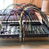
    626A2BF0-C257-4744-B568-FBE30E8A91A9.jpeg

    At these distances, we don't have to worry about transmission line effects, so all connections are unterminated. Here's a trace of the counter output:

    FETSwitchAdder3.3V.png

    We're probing pin 11 on the '163 counter (divide by 16 output), and the carry-chain is configured as two 4-bit segments linked with the AND gate. We can calculate the tpd of the carry-chain based on the 4.29MHz measured frequency as follows:

    • 8-bit carry-chain w/ AND gate: 4.29 MHz x 16 = 68.64 MHz = 14.5ns period / 2 = 7.25ns tpd

    Removing the AND gate from the circuit is pretty much a wash -- the delay from the added capatiance is just about equivalent to gate delay we take out: 

    • 8-bit carry-chain, no AND gate: 7.2ns

    So, we have about 0.9ns per bit. The 12-bit carry chain showed a pretty linear growth in the delay, with 0.9ns per bit as well:

    • 12-bit carry-chain: 10.8ns

    The tpd of the adder includes the carry chain plus the switch-time of the 74CBTLV3253, which is 2.9ns (typical). That will remove one bit from the carry chain, so a net addition of about 2ns. The final inverter in the chain should be counted since the carry chain will need to be buffered from the rest of the CPU. So that gives us about 9.2ns for the “A to C” tpd of an 8-bit 74CBTLV3253 FET Switch Adder (roughly 1.2ns per bit). 

    Not bad at all, and certainly MUCH faster than an equivalent circuit using conventional gates (a conventional ripple-carry adder would be roughly 3ns per bit with NC7SV logic). So a great result, all told, but unfortunately not quite fast enough for 100MHz operation. We’ll have to keep working to squeeze out just a little more performance out of this circuit.

  • The ALU

    Drass10/17/2020 at 18:14 0 comments

    Let's take a closer look at the ALU. The overall structure is actually fairly straight forward:
    ALU Block Diagram.png
    There are registers at the inputs, ALUA, ALUB and ALUC. From there, there are independent paths for the adder and other functions in order to keep capacitance as low as possible for the adder. The shift buffers (SHR and SHL) are placed after the OR function so either the ALUA or ALUB can be shifted by feeding a zero to the other input. Logical operations and shifts are both very fast so there is no issue having them in series. There is a dedicated left-shift buffer rather than using the adder to add a value to itself, as is commonly done. This is so we don't have to connect the A and B inputs of the adder together, which would once again add capacitance.

    The R and C registers at the outputs of the ALU capture the ALU result and carry at the end of the cycle. There are paths that bypass these registers to recirculate R and C back into the ALU inputs. Thse are required when two inter-dependent ALU operations follow one after the other immediately. This is the case, for example, when adjusting the high-byte during address calculation.

    Control signals going to the ALU are applied only at the outputs in order to select the desired ALU operation output. The control signals can therefore be generated without penalty *during* the cycle while the ALU itself is working. The Flags To Modify (FTM) register is used to capture Write-Enable control signals for each flag that must be updated. The flags are actually updated in the cycle following the ALU operation based on the R and C values. The A7, B6 and B7 hold the indicated bits from the A and B inputs and are used to evaluate the V flag.

    The theory of operation for the ALU is that all inputs must be prepared and loaded into registers in the prior cycle. At the clock-edge, the ALU begins working immediately, and the results are captured into output registers at the very end of the cycle. The ALU is thus bracketed by registers on both sides, and can be neatly inserted as a pipeline stage into the datapath. 

    One thing to note is that the ALU does not invert the B input of the adder for subtract operations. Instead, the B input is inverted in the prior cycle. This manouver reduces the propagation delay through the adder and conveniently shifts the burden to the prior cycle -- which is typically a operand read of the SBC instruction. There is plenty of time to invert the operand on the way in from memory.

    And that's a nice segue to the setup for memory: 
    Memory.png
    In this design, memory too has dedicated registers, namely ADL, ADH, WE and DOR (Data Output Register). Just as with the ALU, these registers are also loaded in the cycle prior to the memory operation. The result of a memory read is clocked into a register also. but rather than using a dedicated register, the data read is placed directly into an appropriate internal register in the CPU (ALUB, ADL, ADH or IR).

    This arrangement is very well suited to synch RAMs, which have registered inputs internally. When using synch RAM, ADL, ADH, WE and DOR merely act as shadow registers to the synch RAM's own internal registers. An asynchronous data bus can run at the outputs of ADL and ADH, where traditional RAM, ROM and other peripherals can operate as usual. Of course, very little time will be available for such peripherals in the normal cycle, so it is likely that all aynchronous I/O will be wait-stated (or buffered). More on that later.

    Equipped with these registers, both memory and the ALU can be treated as pipeline stages. In both cases, we set up the inputs in one cycle, the operation is completed in the next, and the result is captured in registers at the end of the cycle. The critical path for the pipeline stage includes the CLK-to-Q delay of the input registers and Data-to-CLK setup time of the output registers. If the output is going directly into synch RAM internal registers (when using the ALU to calculate an address, for example),...

    Read more »

  • Clocking Registers

    Drass10/17/2020 at 16:01 0 comments

    At 100MHz, the cycle is only 10ns long. At that time scale, issues that can go ignored at slower clock-rates suddenly become very material. Clock-skew is one such issue. The cycle is so short that even small delays on clock signals will be material.

    What kinds of delays could we be dealing with? Suppose we have a clock signal internal to the CPU with a 1.2ns rise-time (Tr) driving a 5" trace with ten flip-flops on it. A 50Ω trace on FR4 will present 3.3pF of parasitic capacitance per inch, and each flip-flop will add 3pF of capacitance in addition (assuming AUC logic). The cumulative delay on that trace is something in the order of 3.5ns relative to the input clock signal (i.e., prop delay = Tr + RC, so 1200ps + (5 * 3.3pF * 50Ω) + (10 * 3pF * 50Ω) = 3.5ns). 3.5ns may not seem like much, but it represents more than a third of the cycle at 100MHz!

    The moral of the story is to manage capacitance on clock lines carefully. To that end, I'm contemplating using a CDCVF310 1:10 Clock Driver to distribute the clock around the board. A two level clock tree can provide a dedicated trace for up to 100 destinations with minimum capacitance. We can then adjust for the tpd of the clock drivers themselves by using a CY2302 Zero-Delay-Buffer (ZDB) to synchronize these internal signals to the input clock.

    Beyond capacitance, there are four key specs in the CDCVF310 clock-driver datasheet that we should examine to better understand skew:

    • Tpd = 2.8ns max -- Propagation Delay: CLK input to Yn output propagation delay
    • Tsk(o) = 150ps max -- Output Skew: the variation in the tpd between outputs, i.e., from Ym to Yn
    • Tsk(p) = 250ps max -- Pulse skew: the variation in tpd from PLH to PHL
    • Tsk(pp) = 350ps max -- Part to Part skew: the variations in tpd from various ICs on the board

    With a multi-level tree, all four specs may come into play, and the total skew can add up to be a problem if we're not careful. Consider two Flip-Flops in series, like this:Attachment:

    CLKFF.png

    If the clock-delay from FF1 to FF2 is longer than the tpd of FF1 plus the data delay to FF2, then FF2 will not latch the intended value correctly and the circuit will fail. One way to ameliorate the problem is to use trace delays in our favour. We can wire CLK signals so traces go from downstream flip-flops to upstream ones, hence clocking them in reverse order. Another option is to introduce delay in the data signals until the travel time between the flip-flops exceeds the longest clock-skew by some safety margin.

    And that brings us neatly into the issue of Write-Enable signals (WE) and how they might impact skew. We have a few implementation options to consider:

    1) On the C74-6502, write signals are all routed to a 74AC273 register and released together on the clock-edge -- like this:Attachment:

    CLK273.png

    The 74AC273 is cleared mid-cycle by a low-going pulse. Active-high WE signals arrive at the 74AC273 at various times throughout the cycle, but then travel to their destinations more or less together. A challenge with using this approach in this design is the potential skew between the outputs of the’273 register. There is no spec for skew mentioned on the 74AC273 datasheet, but it can be as much as 1ns on a 74LVC273. (From the datasheet, Tsk(o) = 1ns max, “Skew between any two outputs of the same package switching in the same direction."). In addition, it’s also more difficut to generate the mid-cycle pulse to clear the ‘273 reliably at these clock-rates.

    2) To minimize skew, we ideally want nothing in the path between the clock and a flip-flop’s CLK input, as in this alternative based on a 2:1 FET Mux at the data inputs of a register:Attachment:
    CLKMUX.png
    This method accomodates both active-high and active-low WE signals equally well. The FET switch will add 5Ω of series resistance at the data inputs of the flip-flop, and with it some minimal additional delay that we can safely ignore here. The switch-time of the mux becomes the...

    Read more »

View all 8 project logs

Enjoy this project?

Share

Discussions

Ken KD5ZXG wrote 10/10/2021 at 02:06 point

Lets talk about that FET carry chain. You last mentioned "74AUC2G53". I've been using SN74CBT3253 which are 4way transmission gates, and slower to switch, but less ohms. Similar capacitance.

Every slice of my carry has to slog past the combined capacitance of four TGs and a XOR at roughly 3.5pF each. Wondering: Should I have used a 2way TG to switch between propagate and replace? To skip past 7pF of unneeded generate and annihilate TGs when the propagate path is active. 

Maybe 74AUP for XOR? Slower than AUC, but have 1pF inputs. I question how far can the unbuffered carry chain be stretched before it demands some help? Momentarally forgetting your objectives are 6502, I had something wider in mind.

  Are you sure? yes | no

Ken KD5ZXG wrote 09/19/2021 at 00:01 point

You could precompute (perhaps with a real 6502) byte+byte+c sums or any other ALU functions and flags. Store in <10nS SRAM as cheat-sheets. If an upper byte is needed, speculatively lookup both cases. When C8 becomes known, discard the irrelevant case.

A 16bit incrementer would not need carrys in, out, or between bytes, even if two SRAMs might be required to cover 16bits out. Maybe the spare 17th address bit decrements? With address counting taken care of, you also won't need to speculate an upper byte if all other math and logic inputs are truly 8+8+1 limited.

Surely some cache chips of 9 or more bits wide must exist? Check some old 486 boards. Example below is only 8 bits wide and 10nS, but I havn't searched extensively. Important thing would be 17 or more address input bits. Can always parallel data outputs for greater width and simultaneous flags. Is 6.5nS still the limit when there is no time required to test flags?

Sadly the fastest parallel NVSRAM are only 25nS, and MRAM 35nS. Which might get you 40MHz without having to regenerate or reload tables every boot. Any faster, and lookup tables will have to start from a blank slate.

https://www.cypress.com/CY14NVSRAMKIT-001

Historical precedent would be the IBM 1620 CADET. Stored addition and multiplication tables in core. Infamously shamed as "Can't Add Doesn't Even Try". Has the time come for a 6502 CADET? Slap a Peltier on some 10nS and pray for eight...

----edit----

https://www.mouser.com/datasheet/2/771/8160xxD-976372.pdf

Cheap, non-BGA. 1M x 18bits 5.5nS in Flowthrough mode. Burst doesn't appear mandatory. Enough cache to store sixteen ALU functions with flags and protect mask.

A+B, A+B+1, A-B, (A-B)-1

Same maths again in BCD.

AND, OR, EOR, BIT (BIT throws different flags than AND...)

ASL+0, ROL+1, 0+LSR, 128+ROR

What to do for CMP behaving differently than subtraction?

How to carry a 16bit address + 8bit offset, or are offsets just 7bits with a sign?

--edit--

Was also gonna ask if/how CMP works for BCD? But occurs to me if all BCD CMP does is set flags, it need not function any different than binary CMP. But the flags thrown by CMP are also not exactly same as subtraction.

Yes, 16bits plus 7bits with sign. But a sum address could still cross page boundary requiring carry. Original 6502 allowed an extra cycle when that happened. We want fast or original?

-edit-

If lookups don't satisfy TTL victory conditions (but FET switches somehow do) you might look to a 4bit Manchester Magnitude Comparator for decimal adjust. Which might use the same 74CBT3253 chain, but with borrow propagation through 00 and 11 cases. Or carry with an inverted /B input. Wether we consider /B as subtraction by addition, or a reorganization of the FET chain for magnitude comparison, all the same.

Still, I'm not sure how you discover a decimal half-carry in parallel time with addition? Seems something to be done with a 4bit sum and carry as an afterthought. Though is not a problem for pre-computed lookup tables, since bitwise carries do not actually occur. Or perhaps do once, but only when tables are initially built.

What 74TTL had you planned for 100MHz main memory? Which is why I don't hold ALU tables of the same to be disallowed. Where an Arduino to build tables might be cheating. A real 6502 to build tables feels less cheaty, even if they might be retained in a non-volatile something and never again re-calculated.        

  Are you sure? yes | no

zpekic wrote 10/10/2021 at 09:48 point

I also think fast lookup table is the way to go. In addition, the /P and /G (carry generate and carry propagate) signals could be stored in the table (4 bit result, nP, nG, zero, 1 bit free). This way the 2 nibbles of the ALU (= 2 fast RAMs) do not depend on each other at all. Carry logic is independent and goes through very few AND/NOR gates. The exact logic could be seen in Am2902 and its use, except even simpler because only 2 low stages are needed (Am2902 supports 16-bits, here 8 is needed for ALU, or maybe all 16 if this approach is used for 16 bit incrementer). Even V (overflow) flag can be generated as (Cout3 XOR Cout7). (See page 2-25 here: http://bitsavers.trailing-edge.com/components/amd/bitslice/1979_AMD_2900family.pdf - perhaps an actual fast version of Am2902 could be used?) 

As far as decimal logic, that is of course another address input into the look up table. I have not seen propagate and generate used with decimal add/sub but probably with some modifications could be, just need some crunching of all the valid input / output combinations. I used lookup tables with BCD in one of my projects ( https://github.com/zpekic/Sys_180X/blob/master/CDP180X/nibbleadder.vhd ) . 

btw, are there any programmable ROM-like devices under 10ns access times hobbyists can use, or has to be RAM? In the latter case, what is the approach to bootstrap it?  

  Are you sure? yes | no

Ken KD5ZXG wrote 10/11/2021 at 10:44 point

If both (or more) SRAM have enough address lines for complete 8+8+1 input, and lack only wide enough output, just parallel those outputs. Pre-computed together, each has prescient knowledge of the other's state. No need to pass flags between them at lookup time. A proper overflow would be XOR(C8,C7) and can be looked up without delay for afterthought XOR. Do it all in advance.

When you get to 16bits + an 8bit offset, lookup hits the fan. May not find SRAM with enough inputs for each to be prescient of the other's state. Still not a problem. Real 6502 uses an extra cycle when carry crosses a page boundary. If cycle accuracy matters, no need to complicate this.

But lets pretend the objective is speed. Might want to lookup both cases of upper byte, with and without carry, then discard the case that doesn't apply. Upper lookups can all occur in parallel time without prescience of the lower. Discard might then be a matter of SRAM /OE's or a MUX, whichever is faster...

----

An issue abusing ROMs to mimic Propagate Generate. Even if tables can easily output P G lookahead flags, carry can't be fed back into the same table for a different result. Address inputs have to be held valid, and the change of any one address bit for any reason is a whole different lookup that disturbs every output (including P G). This is not how oldskool ALUs behaved when carry fed back from lookahead logic. Fortunately, carry can be pre-computed and we only need read the result and any flags we care to know, not actually use those flags to do the math over again.

  Are you sure? yes | no

eightycc wrote 10/26/2020 at 19:21 point

Very nice project. One small nit to pick with the writeup: Amdhal's 5990-700 delivered in June 1988 had a 100 MHz clock. In most cases, mainframes got there first. Of course the 5990-700 consumed prodigious amounts of power, floor space (raised floor please), and cost $6.1 million.

  Are you sure? yes | no

Drass wrote 10/26/2020 at 20:56 point

Thanks for the comment. There was also the Fluroinert-cooled Cray 2 supercomputer, clocking in with a 4.1ns cycle (244 MHz) in 1985. I have no idea what it sold for, but I am sure it was not in the “commercially reasonable” category. There may have been others as well, but I’d venture none that were as dramatic looking: :) https://images.app.goo.gl/spzUG5EpmuBcZ2Uj8

  Are you sure? yes | no

Yann Guidon / YGDES wrote 10/27/2020 at 03:02 point

If we're going to talk about Cray's... I'm in.

  Are you sure? yes | no

Jrsphoto wrote 11/05/2020 at 17:58 point

I worked for a company in Eau Clair, WI. in the late 80s and built engineering workstations for Cray in Chippewa Falls, WI.  I frequently got to walk the LONG assembly hallway, with individual clean-rooms on either side of the hallway with Crays in various stages of assembly.  It was quite a site to see.

  Are you sure? yes | no

Yann Guidon / YGDES wrote 10/24/2020 at 20:11 point

At 100MHz you end up with sub-ns edges, that means that you have not only transmission line effects because you shift to the GHz spectrum range, but also you need very careful grounding ! Return currents are very significant at these frequencies and could create ground-bounce effects worse than transmission-line effects. I guess your PCB has a ground plane and a + plane, and you need proper ground vias close to the data/signal vias to help... Yes I've been watching this kind of videos lately :-D https://www.youtube.com/watch?v=nPx2iqmVAHY

The lesson is that single-ended signals have invisible return currents, even differential lines NEED proper grounding.

Looking forward to seeing the rest of your system !

  Are you sure? yes | no

Drass wrote 10/24/2020 at 22:56 point

It's a three headed monster: logic errors, propagation delay and signal integrity all can get you!  VCC and GND planes are a must, and yes one has to be careful when switching reference planes. A lot to think about!

  Are you sure? yes | no

danjovic wrote 10/24/2020 at 01:55 point

Sound? Sure? A 100MHz 6502 is travelling at warp speed!! 

  Are you sure? yes | no

Drass wrote 10/24/2020 at 13:55 point

Yeah, trying to warp time! :) Thanks for the like @danjovic.

  Are you sure? yes | no

Drass wrote 10/22/2020 at 22:00 point

Thanks for dropping by Yann. Always good to hear from you.

  Are you sure? yes | no

Yann Guidon / YGDES wrote 10/23/2020 at 23:51 point

and I'm happy to read you again !

That endeavour sounds exciting... but why don't you use existing monolithic adders ?

  Are you sure? yes | no

Drass wrote 10/24/2020 at 13:53 point

Yes, particularly exciting since the outcome is far from guaranteed! :) It looks feasible, but time will tell.

Regarding the adder, there is only 6.5ns available for the 8-bit adder and 16-bit incrementer. I haven’t found anything in discrete logic that can do the job.

  Are you sure? yes | no

Yann Guidon / YGDES wrote 10/22/2020 at 04:24 point

Oh my.........

  Are you sure? yes | no

Similar Projects

Does this project spark your interest?

Become a member to follow this project and never miss any updates