strange.rand
-
Outdoor test results and random thoughts
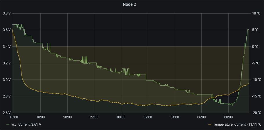
01/19/2021 at 11:54 • 1 commentI've tested the module outdoor for about two weeks and it works great. Yesterday was the coldest night (-17.8 °C), and it passed without any issues.
![]()
Additionally, I'll double-check datasheets for each component to validate the temperature range, but most of them should support -40 °C to 85 °C.
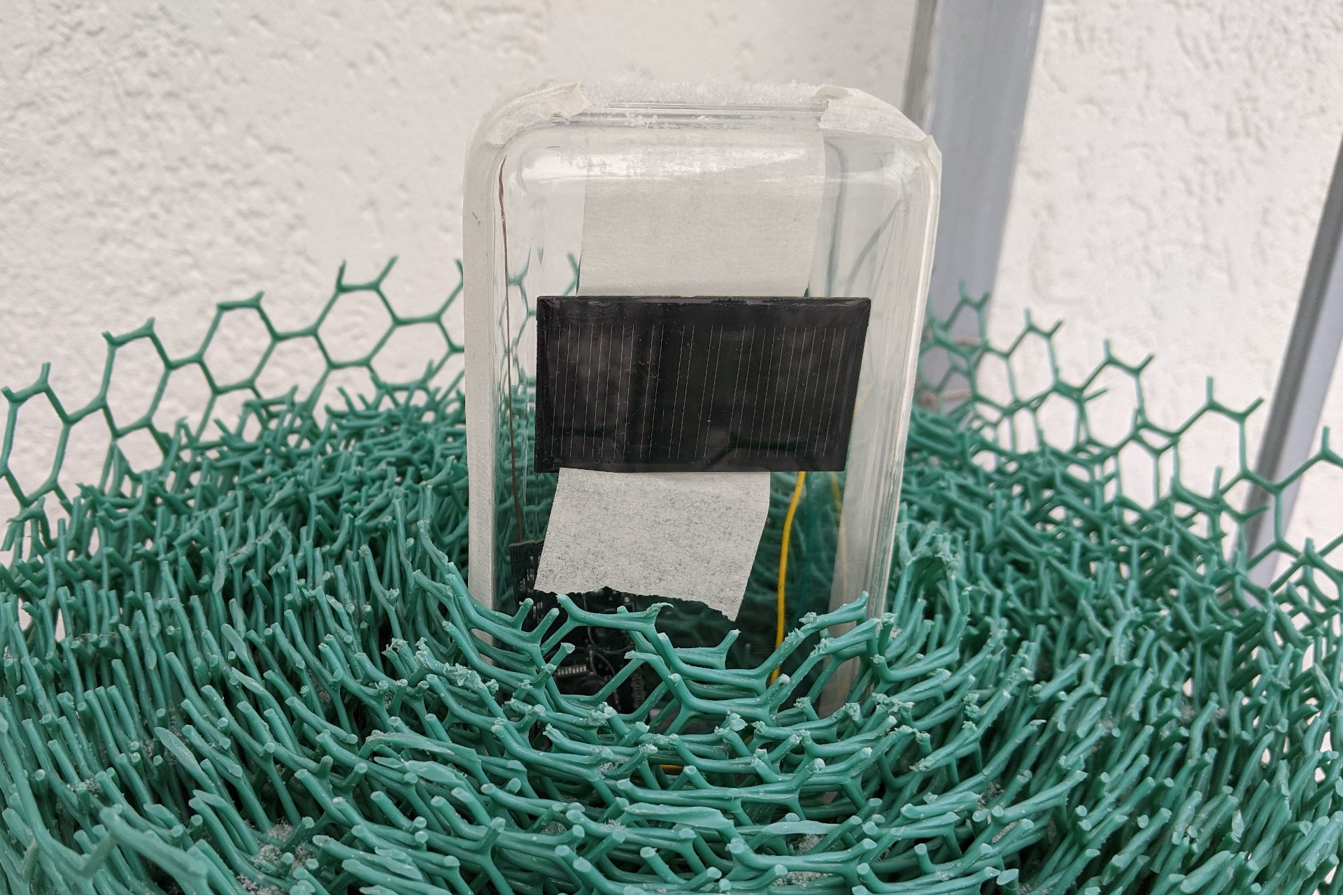
---------- more ----------As I mentioned earlier, in the final version, a 3d printed case should be used, but it isn't ready yet. So for testing purposes, a transparent candy box was repurposed.
![]()
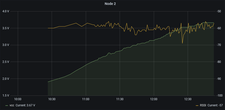
The lowest detected voltage with the current setup was 2.23V, it's okay, but I'll replace the 1F supercapacitor with 1.5F in the future.
During the testing, I accidentally powered off the gateway and turned it on after a couple of hours. The node was discharged much more than I'd expected, but the reason was clear - retries. I use sendWithRetry that by default has 2 additional attempts to send the data. So 3 transmissions instead of 1 per minute during a couple of hours depleted the capacitor much faster. I'll either disable retries or implement smart ones (e.g. if the last 3 transmissions were retried without success - disable retry till the next success transmission).
Currently, I'm waiting for a crimping tool for JST 1.25 connectors, I may use them for connecting the solar panel and the sensor instead of just solder wires. Also, I've found that designing a small and waterproof case isn't something easy. Probably, a much easier way is to fill the whole box with silicone :)
I was asked a few times whether I going to sell this module to makers and hobbyists, and I don't really know. Would you buy it?) The module itself has little sense without a gateway, so probably, I have to finish it first (I already have a vision, almost all components, and a rough 3d model).
-
It finally works
01/04/2021 at 11:02 • 0 commentsThe main info here that the new schematic works as expected and the node's deep sleep power consumption is around 5 uA. Also, I successfully tested cold start (charging supercapacitor from 0V), it looks like this
![]() ---------- more ----------
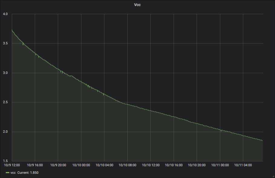
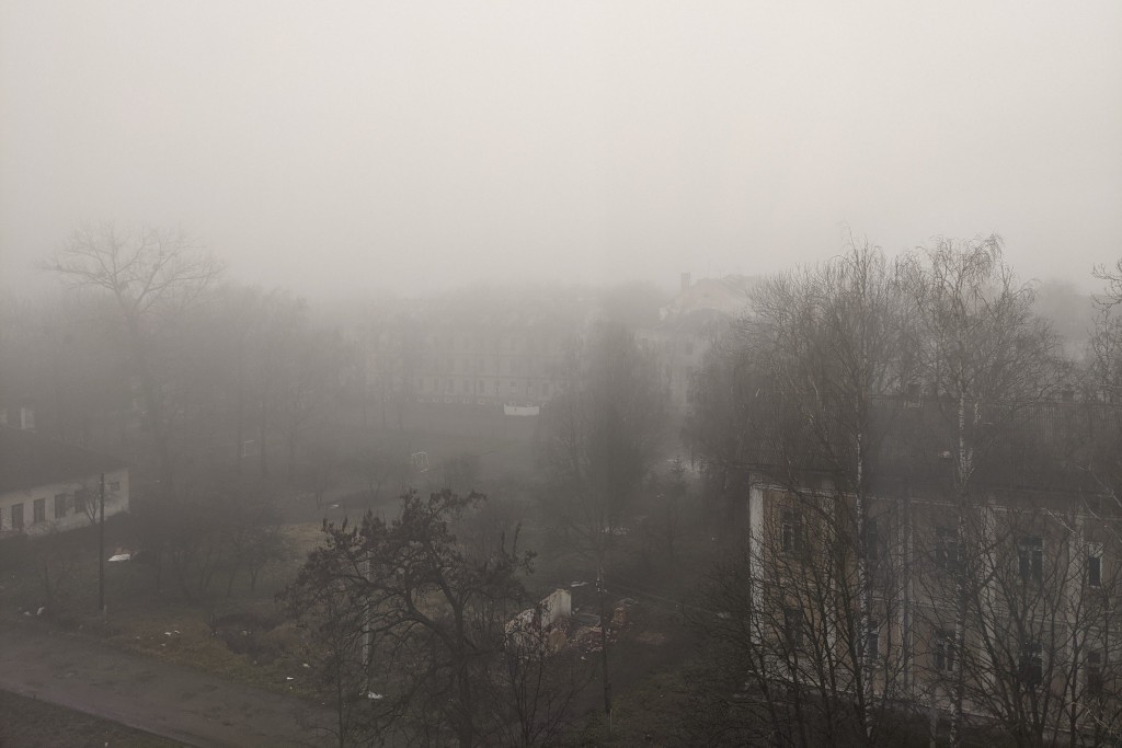
---------- more ----------One more image to understand the weather conditions when Vcc reached 2.5V (there was no fog when Vcc reached its maximum, but still cloudy)
![]()
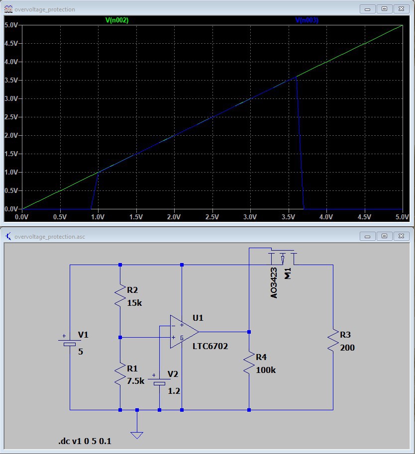
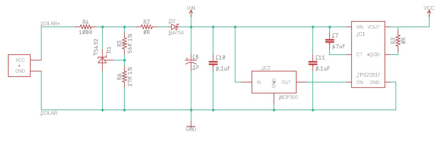
Here is the schematic for over/under voltage protection
![]() R7 shouldn't be 0R, in the previous experiments I used 100R. The VCC line goes to the MCU and sensors.
R7 shouldn't be 0R, in the previous experiments I used 100R. The VCC line goes to the MCU and sensors.As you can see, I've cheated a bit and used a separate IC for switching off the MCU and sensors. Why? There were a few options:
- Low side MOSFET switch
- High side MOSFET switch
- Separate IC
The low side switch is the easiest way to go, but it isn't recommended for switching off MCUs (though, I still think that it might be used in this case).
The high side switch requires a BJT transistor + MOSFET or two MOSFETs and a pull-up resistor. I wasn't sure that using this approach I'll get the required low power consumption, even 1M pull-up causes ~3.6 uA of losses.
The separate IC (TPS22917) advertises operating voltage range from 1V to 5.5V, 2A maximum continuous current (not relevant for this project), and ultra-low power consumption: ON state - 0.5uA, OFF state - 10nA. The IC costs $0.43 on the mouser.
Also, I've ordered separate test PCBs to experiment with the low/high side MOSFET switch, but it'll be later.
Instead of using a separate low ESR capacitor, as I planned before, I ordered a 1F low ESR supercap (the smallest one, physically). Using it, I do not see any significant voltage drop during the transmission. The smallest low ESR supercapacitor that I able to source locally is 15F 2.7V 12.5*27mm (the price is around $1). It's too big, I'll search on aliexpress for something interesting.
![]()
Next steps
- Redesign the PCB one more time (get rid of low ESR capacitor, do not expect "RTC type" supercapacitor)
- Test different sensors
- Design housing for the PCB and sensors
- Create a proper gateway (a separate project probably)
-
Good news & bad news
11/11/2020 at 21:39 • 2 commentsYesterday I received components and soldered test PCBs, then bad news comes out.
I haven't noticed that the chosen voltage comparator has open-drain outputs, so my schematic is incorrect, though I managed to fix it with some wires. In general, under-voltage protection works but consumes from 20uA to 75uA, that's not acceptable. The next try is to use a voltage monitor IC, e.g. NCP300LSN185T1G or something similar.
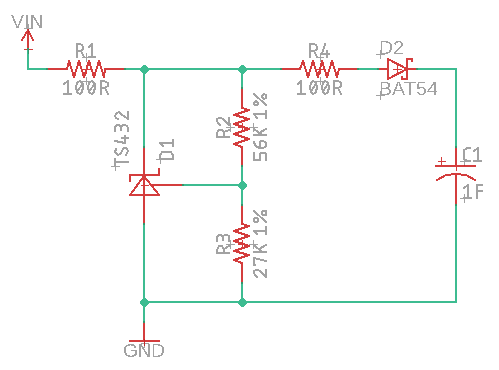
The overvoltage protection circuit is crap. It kinda works, but the overall approach is completely wrong. The circuit monitors a solar panel's voltage and if it < 3.84V (240 mV voltage drop on a schottky diode) it charges a supercap, so we could easily have a case when the voltage on the supercapacitor is 2V, 5V on the solar panel, and charging is disabled :) It can be improved to monitor voltage on supercap, but in this case, it'll drain it (due to voltage divider). The good news here, that the alternative circuit works well (I'll test it more during the next days). It uses an adjustable precision shunt regulator that is capable to output up to 100mA, so basically one IC, a few resistors, and that's all.
![]()
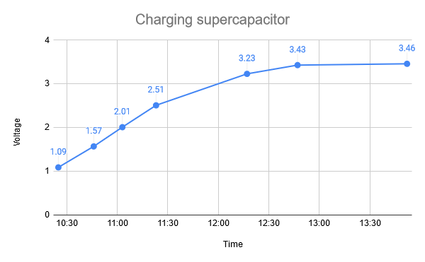
(resistor values aren't final) With this approach, I was able to charge a supercapacitor to 3.46V on a dark and cloudy day using a 53x30mm, 5.5V solar panel.
![]()
So my next steps are:
- Select and order an appropriate voltage monitor for undervoltage protection.
- Design and order new PCBs.
- Test everything again.
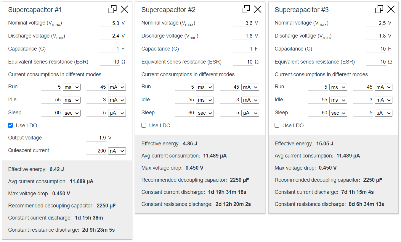
Supercapacitor Discharge Calculator
Recently, I created one more online supercapacitor discharge calculator. All that I've seen don't support different power consumption modes (run, idle, sleep) and some other functionality. It doesn't validate all fields properly, so valid values are required.
![]()
-
Software, PCBs, issues & ideas
11/05/2020 at 14:41 • 0 commentsFirst of all, I'd like to say thank you for all your comments, recommendations, and following the project. It inspires.
Second, you know, giving a meaningful name for the logs is almost as hard as naming variables and methods in programming :)
Software
The node's software has been already published, it uses MIT license to simplify code reuse. The repo consists of two parts: node and gateway. Gateway is based on ESP32. The software isn't 100% reliable and I have a lot of plans for improving it in the future, but currently, it is used as-is to test the node.
The node's software isn't something special too, though I tried to keep it clean and readable. I don't like how the typical Arduino programs are written (everything in one file), so I've separated things a bit. It supports different debug flags that are described in the readme.
---------- more ----------PCBs
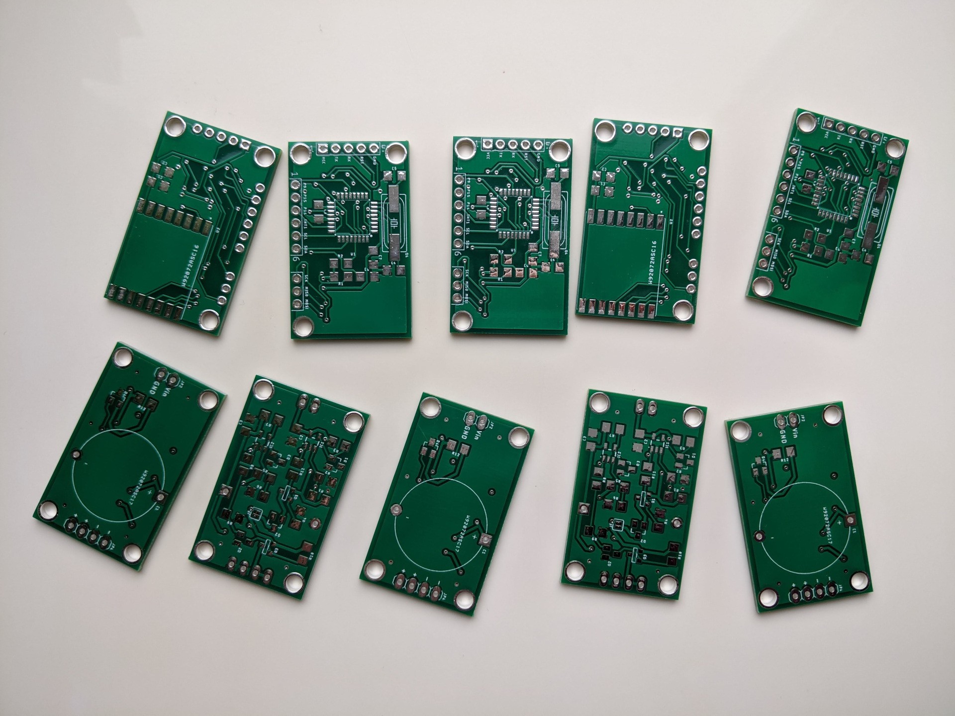
Yesterday I received the PCBs, unfortunately, cannot say the same about the components, still on their way.
![]()
This PCBs aren't the finale ones, I'll use them to test over and under voltage protection circuits.
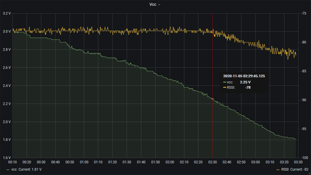
Voltage drop
I've already mentioned it in the previous log, during the transmission voltage on the supercapacitor drops by 0.4 - 0.5V. It is logical, cupercaps ESR equals 10 ohms, the node peak power consumption ~47mA, which gives us 0.047A × 10 ohm = 0.47V.
![]()
From the chart above you may see the result of that voltage drop, we lose transmission power when the supply voltage < 2.25V. Not good at all.
Possible solutions:
- Use supercapacitor with lower ESR.
- Lower a transmission power =D.
- Go back to a previous concept with LDO (but use a better one). It'll allow to use a range from 5.5V to 2.3V.
- Add a low ESR capacitor to eliminate the voltage drop.
- Just ignore it, and live with it (the real world isn't perfect).
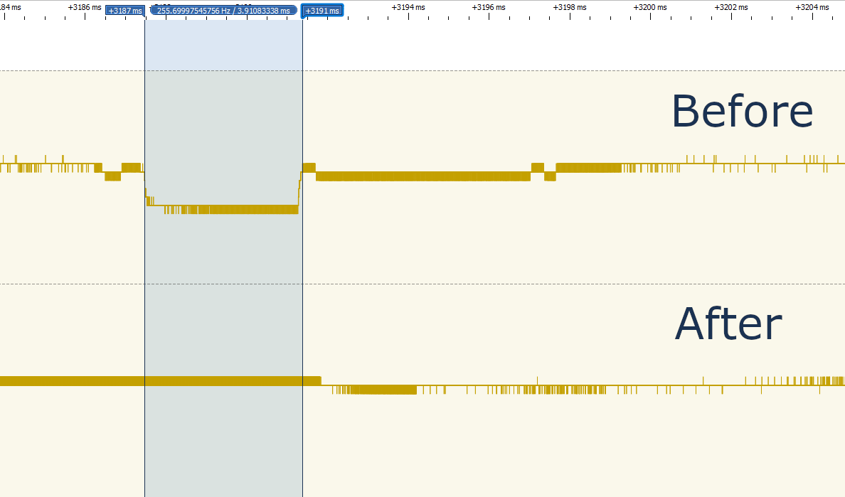
I'll try to use #4 for now. After decreasing a payload size from 17 to 6 bytes (which shortened the transmission time to 3.9ms) and adding a 4700uF low ESR capacitor, I don't see any significant voltage drop during the transmission.
![]()
The downside, it increased the node's power consumption in a weird way. After connecting a 4700uF 16V capacitor and it's initial charging, the node consumes 28uA, after two minutes (at the same supply voltage) 20uA. I'll test it in the long run with a physically smaller capacitor e.g. 4700uF 6.3V (because the current one is really huge and cannot be used in the node).
Sleeping time duration
It isn't a problem, just a fun fact. ATmega328P uses quite imprecise timer for watchdog and deep sleep with the longest period of 8 seconds. But for this particular MCU imprecise mean ~9.135 seconds instead of 8. Didn't expect to see difference in a whole second.
Alternative circuit against over and under-voltage
I really like Martin Held's idea of using a simple voltage monitor IC instead of my schematics, it reduces component count significantly and promises quite low power consumption. I'm definitely going to test it later.
-
Power consumption tuning and other
11/01/2020 at 11:05 • 0 commentsSince I'm still waiting for PCBs and components decided to play a bit with software for the node to optimize power consumption.
Initial values:
- deep sleep: 4 uA
- idle: 2.65 mA
- transmission: up to 45 mA (according to RFM69W datasheet)
First of all, seems I mixed up the power consumption of RFM69W and nRF24L01+ (some time ago I tried to use this transceiver, but then switched to the current one), so now the peak current is around 45 mA, a bit bigger than I initially thought. It's not a big deal, but it should be taken into account.
Measured 4 uA during deep sleep is okay as for me, I use a regular multimeter with 1 uA precision and (0.8% + 1) accuracy so it isn't really precise value. I won't tune power consumption during the transmission part, though it can be easily decreased with decreasing transmission power. And now only one candidate is left - idle mode.
---------- more ----------To program ATmega328P, PlatformIO and Arduino framework are used. By default, in this framework, all periphery is enabled and consumes power, let's try to switch something off. There are two cases: some modules are not needed at all (timers 1 & 2, UART), some required only during a short period of time (SPI, TWI, ADC, etc.).
Due to the microcontroller limitations, I cannot specify a deep sleep period greater than 8 seconds, so every 8 seconds it wakes up to increase a counter and check if the overall sleep duration is greater than required value or no. If yes - it runs the main job, if not - goes to sleep again. During that time all peripheral modules are not needed and should be turned off.
#include <avr/power.h>

ADCSRA = 0; // turn ADC off
power_adc_disable();
power_spi_disable();
power_timer0_disable();
power_timer1_disable();
power_timer2_disable();
power_twi_disable();
power_usart0_disable();
The code above reduces power consumption from 2.65 mA to 2.26 mA, not much, but it is for free.
According to the microcontroller datasheet, all unused pins should be in output mode with a pull-up/down resistor. I already tried this trick to reduce deep sleep power consumption with no effect, but it helps when MCU is working.
#include <Arduino.h>

const uint8_t pins[] = {0, 1, 2, 3, 4, 5, 6, 7, 8, 9, 14, 15, 16, 17};
for (uint8_t i = 0; i < sizeof(pins); i++)
{
  pinMode(pins[i], OUTPUT);
  digitalWrite(pins[i], LOW);
}
This code reduces power consumption to 1.95 mA.
We could save a bit more power disabling modules right after using them, e.g.:
- turn on all required modules
- read power supply voltage
- disable ADC
- read sensors data
- disable TWI
- send data to a gateway
- disable rest of modules
I would say that it looks like over optimization, but it is possible and not really hard. The final node's software will be open source and will be published on my GitHub closer to the final stages of the project.
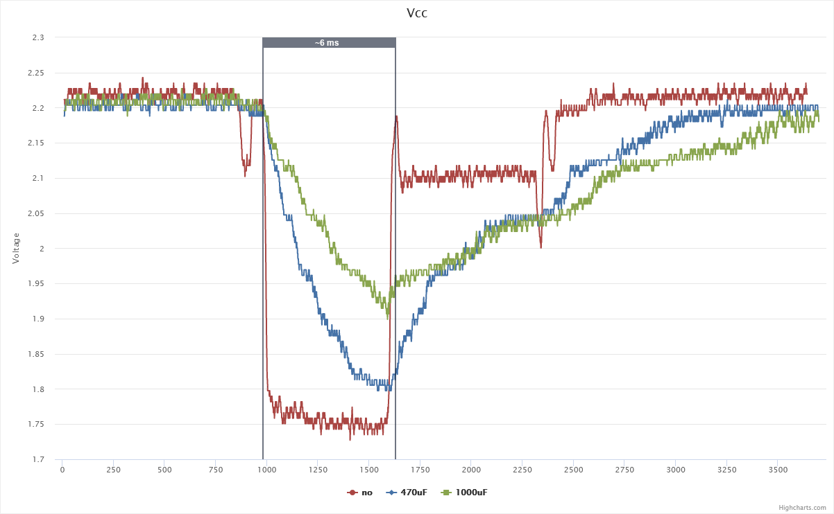
An additional experiment
A few days ago Tomáš asked a good question about supercap's ESR and max current. Initially, I thought that ~25 mA in a peak shouldn't be a problem, but then ~25 mA were transformed into ~45 mA, and I decided to check.
![]()
The chart above shows the voltage on the supercapacitor during the data transmission. There are three series:
- no additional capacitor (except decoupling one)
- 470uF close to the transceiver
- 1000uF close to the transceiver
As you can see, transmission takes about 6 ms, and without an additional capacitor voltage drops by ~0.5V. Surprisingly, when supercapacitor is discharged to 1.8V the node is still functional and sends data. I suspect that transmission power at those stages could be lower, so currently, I'm collecting RSSI for each data package to prove or disprove this (with less power RSSI should be smaller).
That's all for now.
-
Trial and error
10/22/2020 at 20:52 • 15 commentsLet's start from the beginning. I live in an apartment that faces south and west so I can get reliable temperature measurements from a standard thermometer (you know, such thing on your window with a little bit of colored ethanol inside) only till 1-2 PM. That's why I decided to start this project.
The initial idea was to keep it simple and cheap. Components:
- ATmega328P microcontroller
- RFM69 transceiver
- HTU21 temperature and humidity sensor
- 1F 5.5V supercapacitor
- Some solar panel
The ATmega328P microcontroller in a deep sleep consumes tiny amount of energy ~4uA, but to operate at the lowest voltage (1.8V) 4MHz oscillator should be used.
---------- more ----------![]() The next thing to check is the voltage range of the used components:
The next thing to check is the voltage range of the used components:- Supercapacitor: 0 - 5.5V
- MCU: 1.8 - 5.5V
- Sensor1: 2.1 - 3.6V
- Sensor2: 1.5 - 3.6V
- Sensor3: 1.5 - 5V
- RF transmitter: 1.8 - 3.6V
- Solar panel 0 - 5.5V
The easiest way was to use a low-drop voltage regulator and get a stable supply voltage (3.3V) for all components. But after a bit of testing I found out, that when the voltage drops below ~3.3V LDO becomes inefficient and consumes an additional 20uA (or even more) that's drain supercap too quickly.
An alternative solution will be charging supercapacitor to 3.6V max and do not use any voltage regulators. It's much more efficient and in such a configuration I achieved 42 hours of work from a 1F supercap.
![]()
Saying this I should highlight, that the node sends data every minute when the voltage above 2.7V, and every 3 minutes in other case.
At this stage, two additional problems should be solved:
- Overvoltage protection
- Undervoltage protection
Overvoltage protection
I have a bunch of different solar panels, the smallest one, which I plan to use in this project, at the direct sunlight produces 5.5V without the load and can produce more than required 3.6V with the load, so it should be limited somehow.
![]()
I always try to use the easiest solution, but usually, it doesn't work =D. In this case, the easiest option was to use a zener diode, but to work properly zener diode requires some amount of current through it (this can be around 5 to 10 mA), and if this requirement is violated it works non-linearly. For my project, 5mA (continuously) is a huge amount of energy. In most cases, the solar panel won't produce more than 0.5 - 1mA, as I don't expect to see the direct sunlight on the node (for obvious reason, it is a thermometer).
By now, I've already had a circuit for the undervoltage protection based on a voltage comparator, so decided to use a similar approach here. The image below shows the base schematic and LTspice simulation results.
![]()
The circuit isn't perfect. When the supercapacitor is discharged and the solar panel produces 5V, it'll continuously switch on/off charging at the point near 0.9V. I'm not sure that this is a significant disadvantage, it almost like MPPT (except that it won't be the max point). I'll test it in real-life to see how it works or does it work at all.
Undervoltage protection
At some stage of the supercapacitor discharge, we will face the situation when the voltage is too low (<1.8V) and the node should be shut down. ATmega328P includes built-in brown-out detection (BOD) that keeps MCU in the reset state when the voltage is less than some threshold, but it has a price.
Let's imagine a situation: a supercapacitor is fully discharged, a solar panel produces 5V 1mA. Everything is okay at first glance, the solar panel should slowly charge the supercap, and when it reaches 1.8V BOD turns the MCU on. Spoiler alert: it won't work! In the reset state, the MCU consumes an unstated amount of current (3-5mA according to my experiments) and it'll eat all available energy preventing the supercapacitor from charging. That's why external low-power undervoltage protection is required.
With the big help of r/AskElectronics subreddit and u/bigger-hammer in particular) this circuit has been created
![]()
The green line is a supply voltage, read one is a voltage on the load.
In both circuits, I'm going to use a different voltage comparator with better parameters and lower power consumption, but it isn't available in LTspice.
What next?
I've ordered PCBs and required components, but they haven't arrived yet. All those things should work in theory, but will they? A separate question is: what will be the final power consumption with all those additional components? Will see :)
PS
If you see grammatical or structural mistakes, please PM me.
Wireless solar-powered sensor node
A solar-powered node that stores energy in a supercapacitor, wakes-up regularly, measures different parameters, and sends them to a gateway
 R7 shouldn't be 0R, in the previous experiments I used 100R. The VCC line goes to the MCU and sensors.
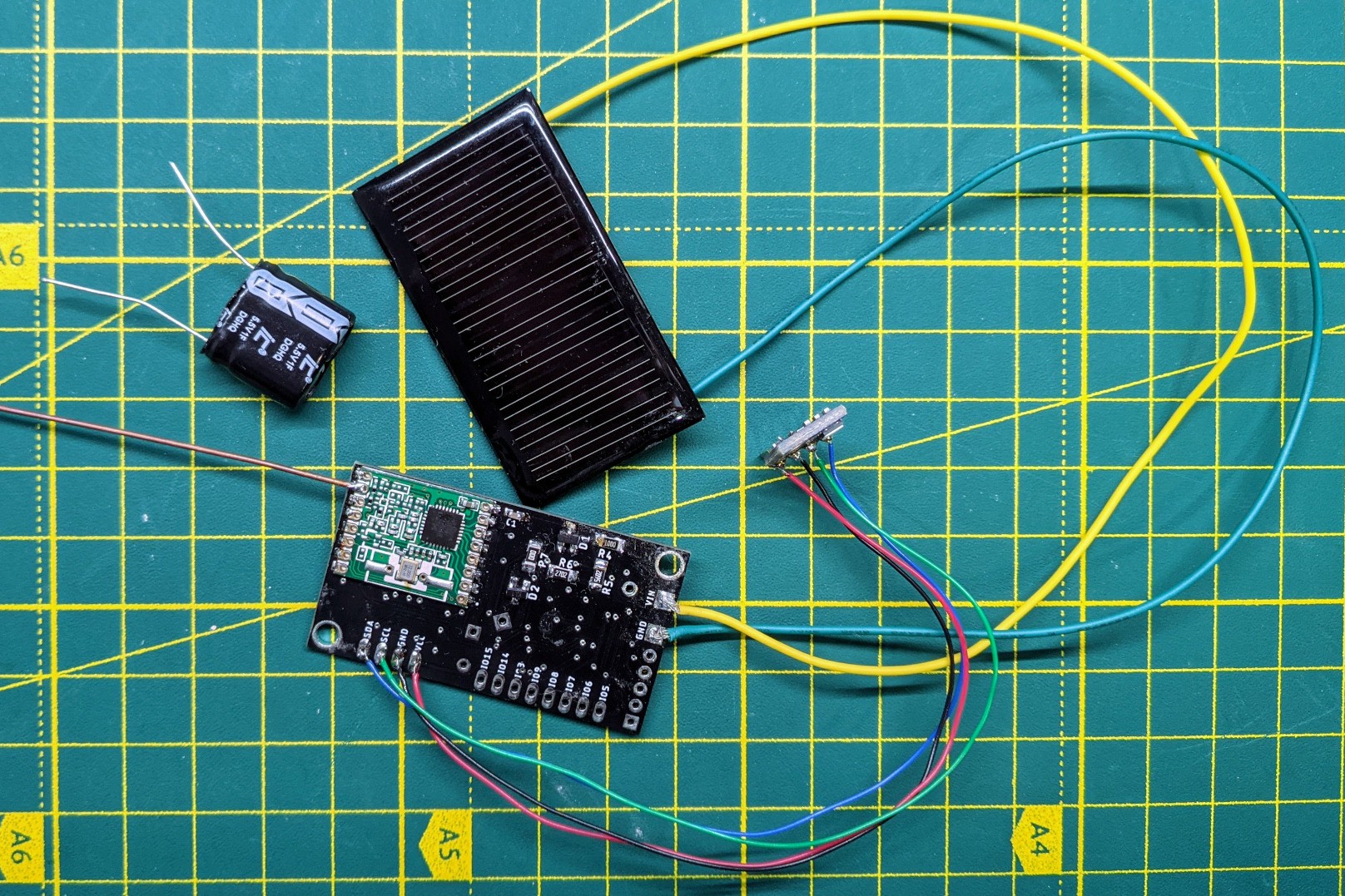
 The next thing to check is the voltage range of the used components: