zpekic
-
Dual video generation (VGA / TIM)
05/03/2024 at 11:51 • 0 commentsProblem statement
An international group of retro-computing enthusiasts came together to recreate the original TIM-011 hardware (details here), at which point the TIM-011 original video circuit became a focus of interest too. There are two main problems with TIM-011 video:
- Non-standard timing of HSYNC and VSYNC signals, which confuse lots of digital input monitors even if they could take the 16kHz video signal otherwise
- No physically compatible connection with any known connector - just 5 pins poking out from the PCB
In original TIM-011, none of the above was a problem, because a special "paired" monitor was used.
Looking at the details of TIM-011 video circuits, it dawned on me that with some extra logic on the PCB, standard 640*480 VGA signal could be generated - in addition to the TIM-011 video, but not at the same time. This project log is a description how it could be done - not only for TIM-011, but maybe for "home brew" computers, as the video circuitry is extremely "vanilla" and requires only basic 74xx ICs and few passive components.
Video signal summary
Regardless of the video format, a same set of signals is needed, but their frequency and timing must be different. Table below summarizes the signals and their values. Uxx refers to "virtual IC" in the FPGA implementation in VHDL.
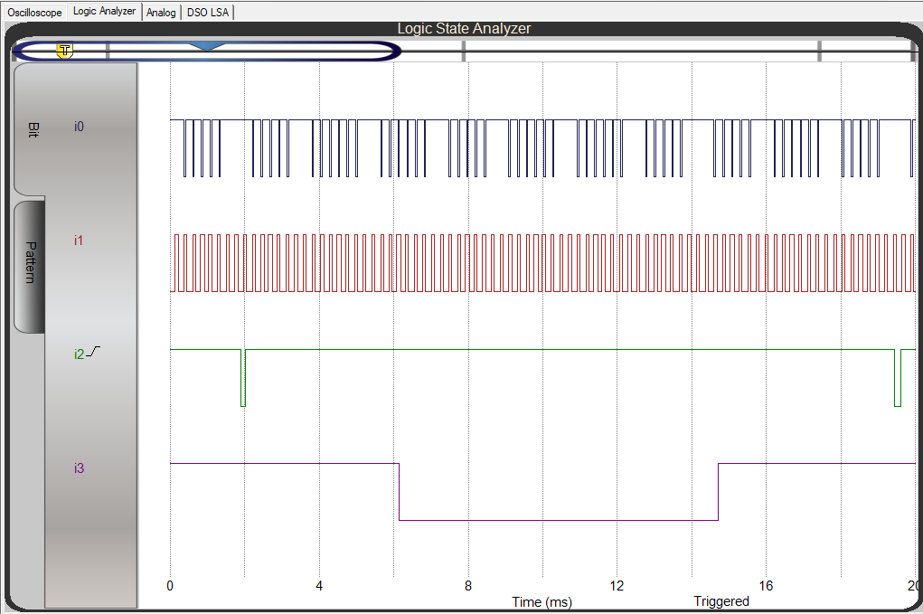
Signal name (or key value) TIM-011 VGA Notes MODE 0 1 External signal (generated by software, or hardware switch or jumper) to select which video signals should be generated PIXCLK (HCLK) 12MHz 24 or 25MHz It is also the "horizontal" pixel dot frequency. 50% duty cycle HRESET 768 800 Single pulse 1 PIXCLK long is generated at this count, determining the length of horizontal scan line.
Resets U13A (horizontal scan counter)HS 576 ... 639
active high0 ... 95
active lowHorizontal sync signal timing is critical for CRTs to recognize and adjust to video signal. @msolajic provided updated TIM-011 values, while VGA ones are well known standard values. HBLANK 512 ... 768 0 ... 255 and 768 ... 800 Horizontal blanking signal (active high) keeps the horizontal pixel counter (U13A) at 0, while at the same time "masking" the V1 and V2 digital video outputs. VCLK HS
f = 15.635kHz/HS
f = 31.25kHzBecause vertical scan and pixel counters are implemented using 74HC4040 which are clocked on falling edge, in case of active low HS for VGA, it has to be inverted. Scan frequency is PIXCLK / HRESET VRESET 320 525 Single pulse 1 VCLK long is generated at this count, determining the length of the (non-interlaced) frame.
Resets U3A (vertical scan counter)VS 280 ... 319
f = 49Hz0 ... 3
f = 60HzVertical sync signal - during this time CPU can read/write VRAM or update the scroll offset register. Frame frequency is VCLK / VRESET VBLANK 256 ... 320 0 ... 127 and 384 ... 525 Vertical blanking signal (active high) keeps the vertical scan line counter (U3A) at 0, while at the same time "masking" the V1 and V2 digital video outputs.
Keeps U3 (vertical pixel counter) at 0.Horizontal pixel range 0 ... 511 0 ... 511 bits 1 and 0 select 1 out of 4 pixels in the byte, giving 128 bytes (7 bits) in the VRAM address schema:
1HHHHHHHvvvvvvvv (MSB is 1 because 32k VRAM I/O space is visible to CPU from 0x8000-0xFFFFVertical pixel range 0 ... 255 0 ... 255 Vertical pixel counter is mapped to lowest 8-bits of the address. This allows easy hardware vertical scroll by adding to this value an 8-bit offset.
1hhhhhhhVVVVVVVVAnalyzing the signal comparison table above, one possible hardware solution becomes apparent:
- Introduce a 8-bit wide 2 to 1 MUX to select the signals above, and the selection is the MODE signal
- Keep the existing horizontal and vertical pixel counters (U13 and U3) as the VRAM addressing does not depend on the MODE, but use them only for that, not any other signal generation. So U13 and U3 always cover only 512*256
- Introduce 2 additional 74HC4040 counters (U13A and U3A) which cover either 800*525 or 768*320 depending on MODE, and use these to generate all the HS, VS, HBLANK, VBLANK, HRESET an VRESET signals.
- To simplify signal generation, two 3-to-8 74x138 decoders (U13B and U3B) are driven by U13A and U3A - these allow "slicing" horizontal and vertical pixel counts by 128 increments.
- All other parts of video circuit remain unchanged, such as V1 and V2 generation, scroll register, latching VRAM data byte at read or write etc.
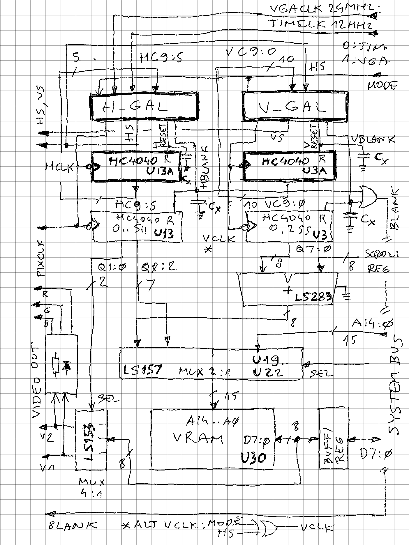
![]()
Dual-mode video high-level schematic. Bold border ICs are additions to original TIM video (rest of circuit is unchanged)
TIM-011 mode
As I didn't have legacy CRT at hand (for example Sony CPD-1302) I used the Gonbes GBS-8200 to convert 4 signals to VGA (code from top-level VHDL component):
-- Connect to GBS8200 gray wire (composite sync!)
    gr_csync <= gr_hsync xor (not gr_vsync);
    GBS8200_GRAY <= gr_csync when (sw_mode = '0') else '0'; --gr_hsync xor (not gr_vsync);

-- connect to GBS8200 blue / green / red wires
-- colors: black, blue, green, white
    GBS8200_BLUE <= gr_vid1 when (sw_mode = '0') else '0';
    GBS8200_GREEN <= gr_vid2 when (sw_mode = '0') else '0';
    GBS8200_RED <= (gr_vid1 and gr_vid2) when (sw_mode = '0') else '0';
Some notes:
- Output signals are kept permanent 0 in VGA mode (to prevent higher frequency VGA signals driving the lower bandwidth video output)
- GBS-8200 takes composite sync, not 2 independent HS and VS signals, so they are simply combined using XOR
- RGB digital video allows for 8 colors, but TIM-011 only generates 4 levels (each pixel takes 2 bits, 1 VRAM byte = 4 pixels). In other words, any 4-entry "palette" out of 8 possible colors can be obtained. In the very simple scheme from the code above, colors will be:
- 000 - black (V1 and V2 both off)
- 010 - green
- 001 - blue
- 111 - white (V1 and V2 both on)
![]()
![]()
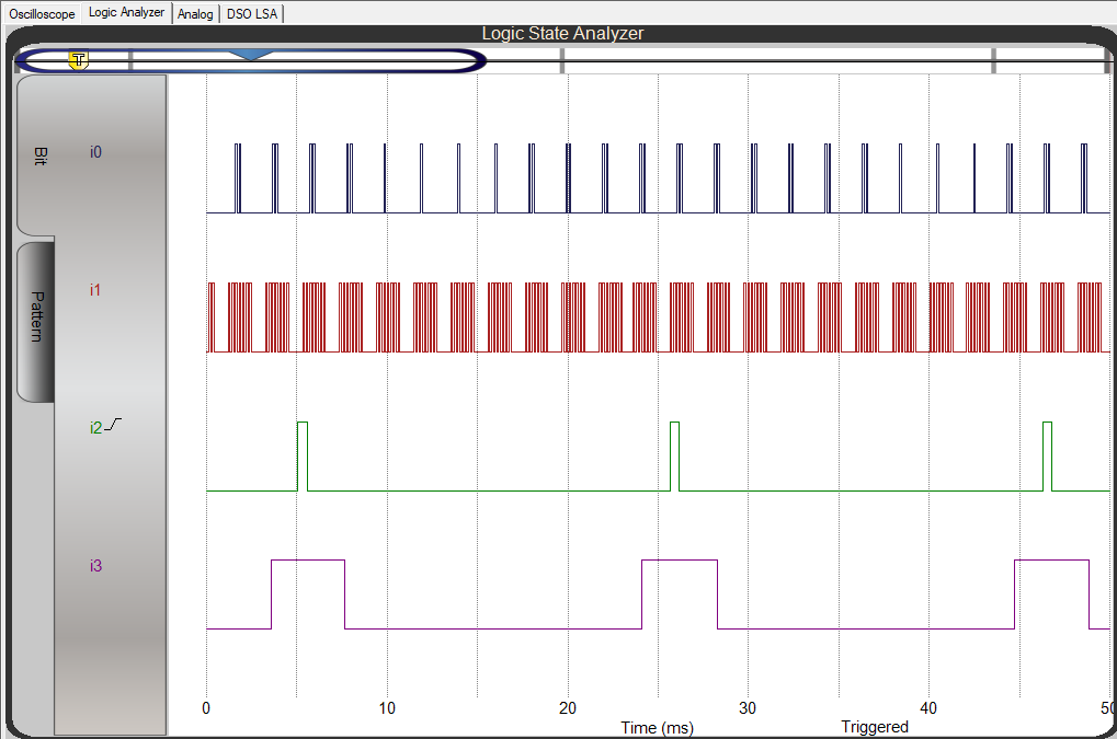
TIM mode HS(ync) and HBLANK (HSync is positive, duration is 64 dot clocks @12MHz = 5.64us; HBLANK is simultaneously reset signal for horizontal counter U13A)
![]()
TIM mode VS(ync) and VBLANK (VSync is positive, VBLANK is simultaneously reset signal for vertical counter U3A )
![]()
VGA mode
VGA signal is generated directly from FPGA. Note the 2:1 aspect ratio (as TIM-011 resolution is 512*256 pixels) centered into 640*480 VGA pixel window (margins are "blanked" using the HBLANK and VBLANK signals explained in the table above).
From top-level VHDL component:
-- VGA connections
-- colors: black (000), dark gray (333), light gray (CCC), white (FFF)
    gr_color <= gr_vid2 & gr_vid2 & gr_vid1 & gr_vid1;
    HSYNC_O <= sw_mode and gr_hsync;
    VSYNC_O <= sw_mode and gr_vsync;
    RED_O <= gr_color when (sw_mode = '1') else X"0";
    GREEN_O <= gr_color when (sw_mode = '1') else X"0";
    BLUE_O <= gr_color when (sw_mode = '1') else X"0";
Notes:
- Output signals are kept permanent 0 when in TIM mode (to prevent VGA monitors to "autodetect" in vain)
- This FPGA board can generate 4096-color VGA (each component 4-bit, 16 values), so 4 out of 4096 colors are possible. Simple connection solution in the code above allows generating 4 levels of gray which is close to original TIM-011 approach.
![]()
![]()
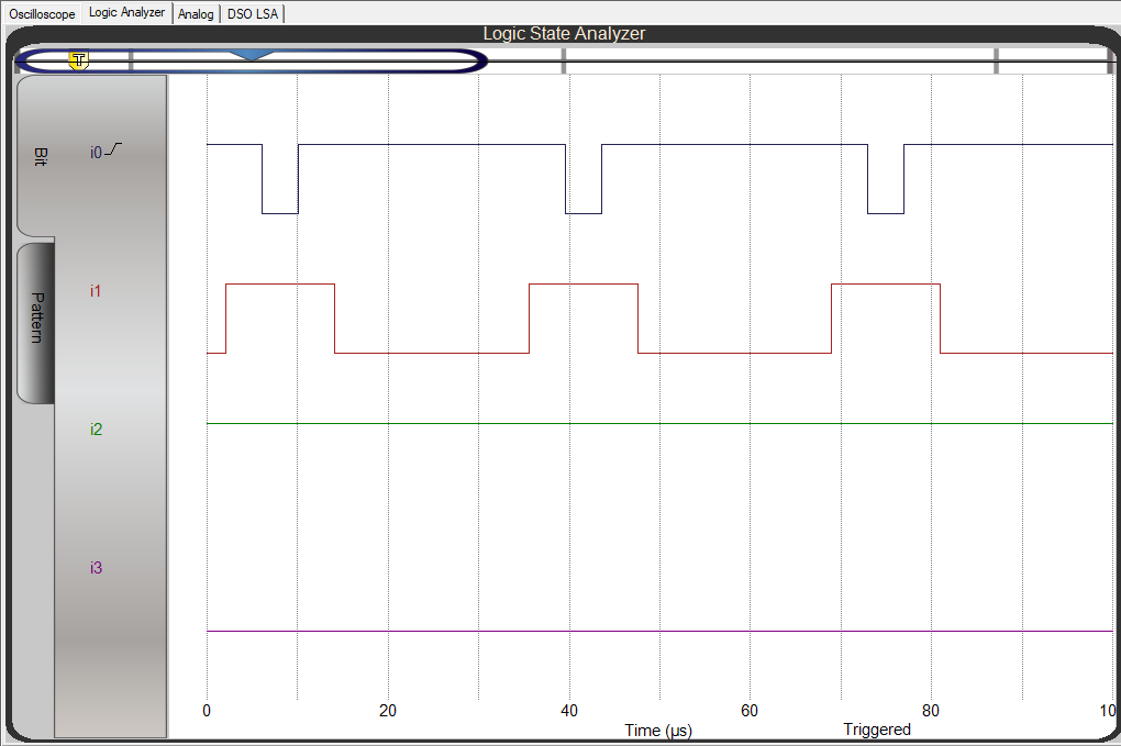
VGA mode HS(ysnc) and HBLANK (HSync is negative polarity, horizontal counter U13A can only count 0..511 when HBLANK is low)
![]()
VGA mode VS(ync) and VBLANK (VSync is negative polarity. Vertical counter U3A can count from 0 .. 255 only when VBLANK is low)
![]()
-
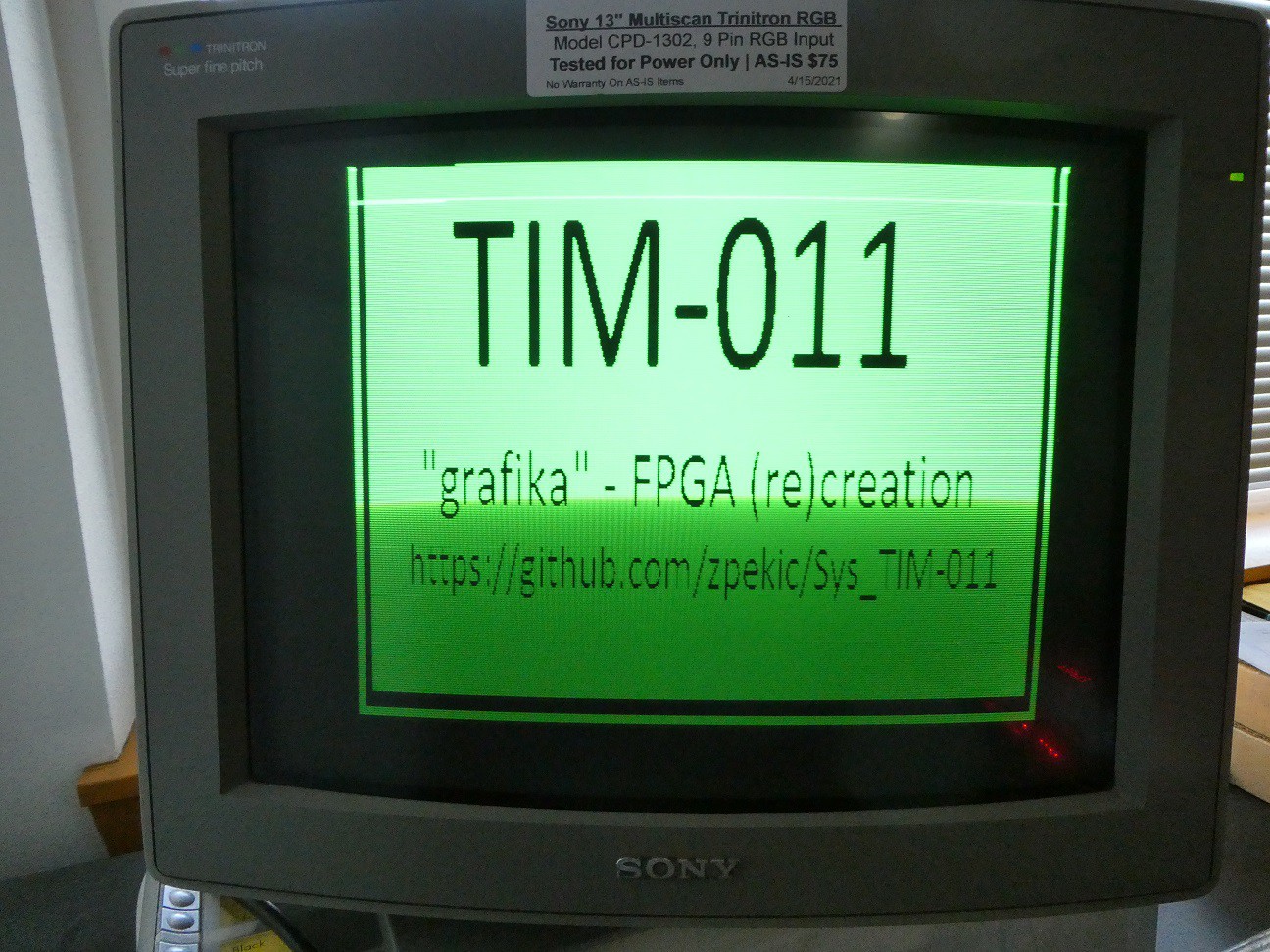
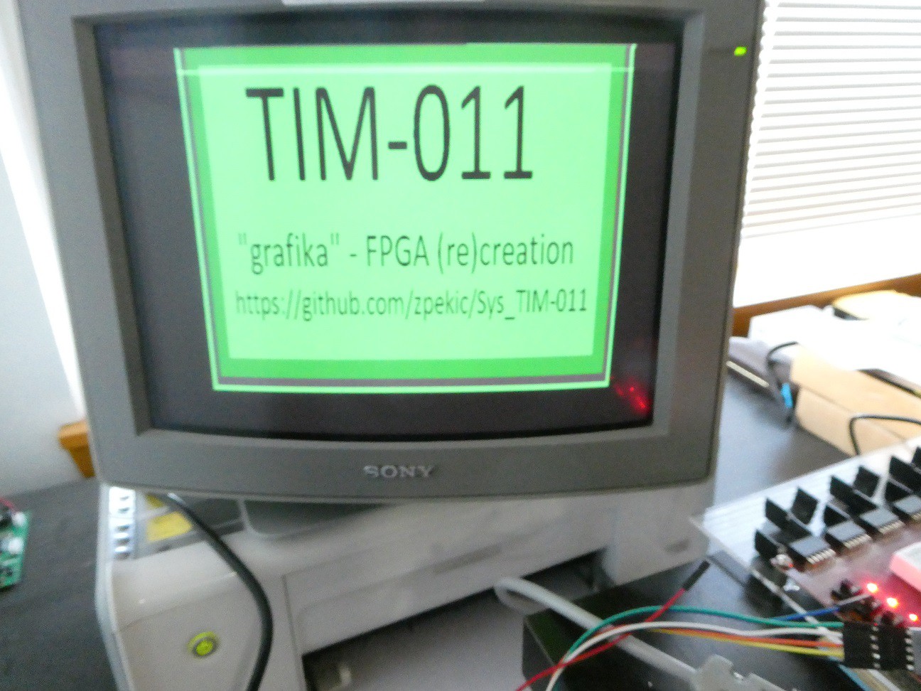
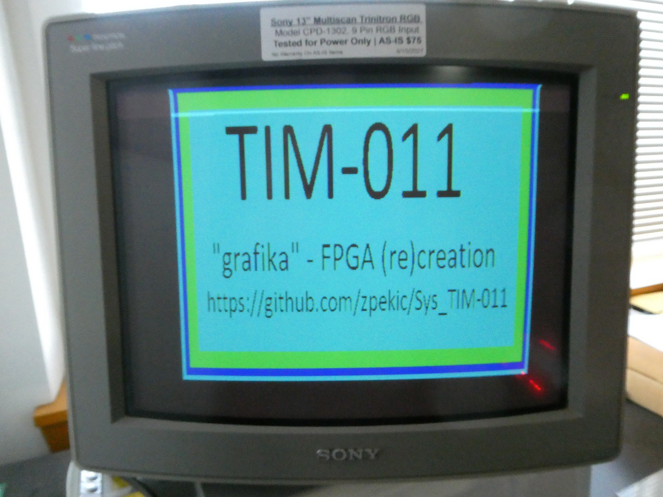
TIM-011 video on Sony CPD-1302
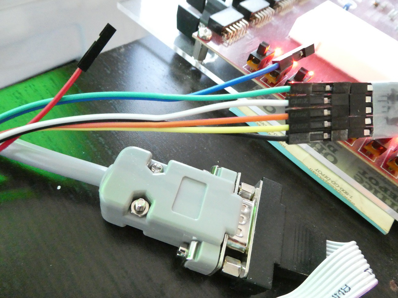
05/10/2021 at 01:40 • 0 commentsI was hunting at the local PC-recycle for a monitor that could be connected directly to my vintage C-128 natively without the usual converter (Gonbess + other) and cable mess. I could not believe my luck when I found a Sony CPD-1302 with Trinitron tube (good old particle accelerator!)
This monitor appeared in the ideal moment when the classic home computers from the 80ies were still around, but the PC revolution started - VGA was expensive and tied first to PS/2, most PC users had MDA, CGA or EGA (all digital) - or maybe PGA which was always a rarity given how high-end expensive it was (analog to be able to produce 256 colors). This monitor supports all of them:
- Analog mode (R, G, B, VSync, HVSync)
- Digital mode (3 different variations, from 4 monochrome "intensities" to 16 colors I, R, G, B, plus VSync and HVSync)
Looking at the CPD-1302 timing charts, it looked that the timing would match:
- Horizontal: 63.78us for CGA vs. 64us for TIM-011 video signal,
- Vertical: 50Hz for CGA (16.65us) vs. 55Hz (18.424us) for TIM-011.
Most importantly (where many vintage computer / monitor pairings fail), the CPD-1302 has a "smart" detection of VSync, extracting it from composite HVSync, or it can be fed directly.
Connection was simple:
TIM-011 CPD-1302 Color (on CPD side reference pics below) GND GND black VSYNC HVSYNC orange HSYNC HSYNC yellow V0 one out of R, G, B, I red, green, blue, intensity is white V1 one out of R, G, B, I red, green, blue, intensity is white Here are some experiments:
Analog mode
Connecting "I" for a color as expected rendered only 2 color image as the "intensity" digital signal is ignored. But the other color signal (green in this case) is recognized as "analog".
![]()
![]()
Digital
With the same I + G switching to "digital" mode, suddenly 4 "colors" appear, as expected. However one would expect black, and 3 shades of green but monitor shows the darkest green as brownish/grayish?
![]()
Now replacing the I+G with B+G:
![]()
As expected, this allows black, blue, green and cyan:
![]()
Summary
In all probability, CPD-1302 would work well with a "real" TIM-011, as it works in all modes (even analog!) with the FPGA implementation of its video circuit.
There was a problem with vertical sync - as seen above the frequencies are somewhat different. This caused flicker, until the image was adjusted towards top of screen. This made the picture stationary but lost few top line of the screen. Not a too big problem in text modes (as the action happens near the bottom of screen) but annoying for graphics or games.
-
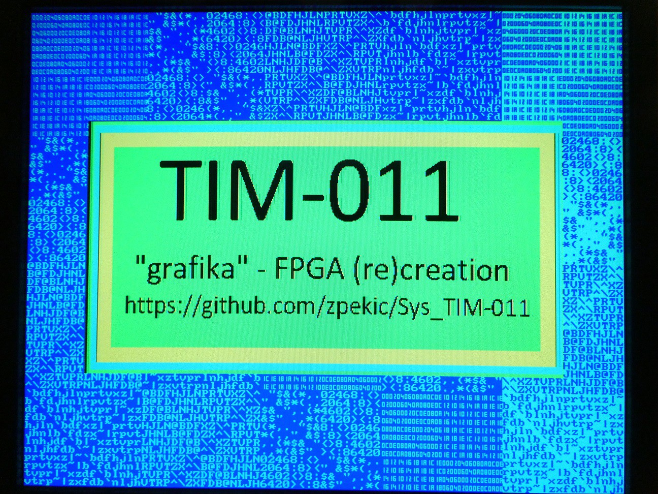
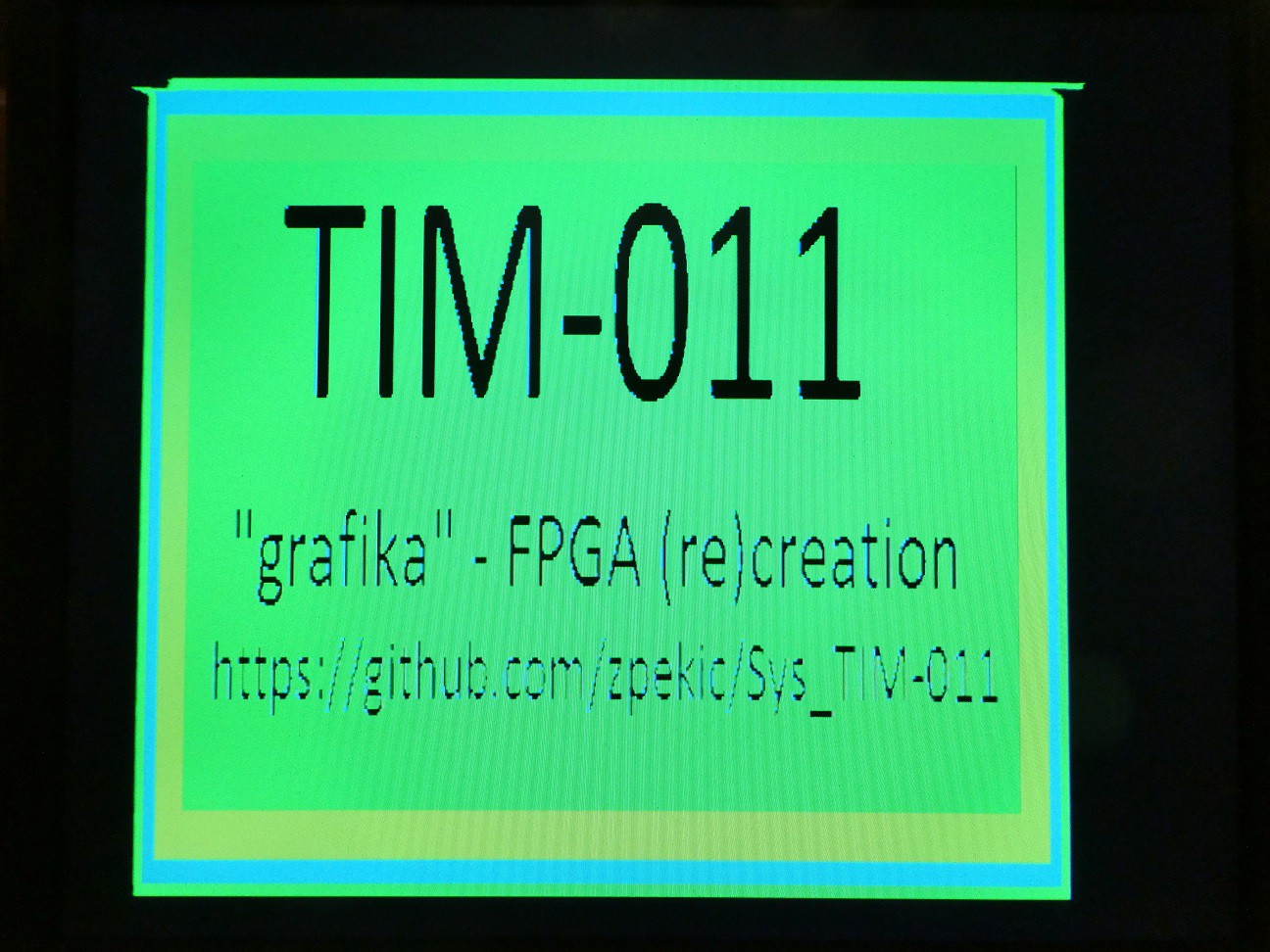
Notes about video quality and sampling approaches
01/07/2021 at 22:00 • 0 commentsWhile overall the sampling of TIM-011 video signal works, and is visibly displayed on the screen, it still has problems:
- first column pixel is displayed (black instead) because there is no real pixel pipeline (and consequently, the last pixel column is not displayed
- there are some random "ghost artifacts" (vertical bars)
Perhaps not clearly visible, a picture from the VGA screen (generated by sampler + VGA controller):
![]()
Now looking at screenshot from GONBES-8200, it has different problems:
- top few lines dancing
- distorted height / width ratio
![]()
So in some ways, both are "worse" but the vertical bar artifacts are very annoying. I haven't tested if those would prevent reading of text on the TIM-011 display.
First, I thought that the image would deteriorate going from left to right, due to the skew between video signal to be sampled and the sampling clock - after all they are synchronized only once per line using hsync signal, and by 512th video signal (or 2048th sampling clock) they could be slightly off. But that is not the case, the quality is evenly good (or bad).
So the artifacts must come from the sampling approach itself. To "debug" it, I feed the sampler with 6 extra signals that control the sampling.
tim: tim_sampler port map (
		reset => RESET,
		clk => freq48M, -- 48MHz (4 times oversample of 12MHz)
		hsync => TIM_HSYNC,
		vsync => TIM_VSYNC,
		v2 =>	TIM_VIDEO2,
		v1 => TIM_VIDEO1,
		a => sampler_a,
		d => vram_dina,
		--limit => switch(7 downto 2),
		-- best result with sampler "algorithm"
		-- s2 from raising edge sample
		-- s1 from raising edge sample
		-- 4 out of 4 sample: on
		-- 3 out of 4 sample: on
		-- 2 out of 4 sample: off
		-- 1 out of 4 sample: off
		limit => "111100",
		we_in => we_in,
		we_out => sampler_wr_nrd
	);
The two MSB of the (not very well) named "limit" are consumed by the tim_sampler.vhd to select if for the v1, v0 video signals should be captured at the rising or falling edge of the sampling clock (s2 and s1 are 16-bit shift registers, clocked at 4*12MHz rate and ingesting the TIM-011 v1 and v0 video signals):
generate_s: for i in 15 downto 1 generate
begin
	s2(i) <= s2r(i) when (limit(5) = '1') else s2f(i);
	s1(i) <= s1r(i) when (limit(4) = '1') else s1f(1);
end generate;
s2(0) <= v2;
s1(0) <= v1;
Answer: raising is much better for picture quality.
The 4 LSB are consumed in the "voter" circuit which gets 4 sample bits (per pixel) and has to decide if those 4 indicated "signal on" or off. It does that by looking at the sampled patterns:
	with value select vote <=
		limit(3) when "1111",	--4
		limit(2) when "1110",	--3
		limit(2) when "1101",	--3
		limit(1) when "1100",	--2
		limit(2) when "1011",	--3
		limit(1) when "1010",	--2
		limit(1) when "1001",	--2
		limit(0) when "1000",	--1
		limit(2) when "0111",	--3
		limit(1) when "0110",	--2
		limit(1) when "0101",	--2
		limit(0) when "0100",	--1
		limit(1) when "0011",	--2
		limit(0) when "0010",	--1
		limit(0) when "0001",	--1
		'0' when others;	--0
Obviously, if no bit was sampled "1" then the output must be "0" - this is the last, default line. But what if it was sampled one of more times "1"? In that case, the output is controlled by selecting on or off individually each combination with 1, 2, 3, or 4 bits sampled "1" (a simple 16->1 MUX).
Through visual experimentation, turns out the best result is enable 4 and 3 bit "1" sample combinations, but not the 2 and 1 bit ones (1 results in unstable pic, 2 is effectively a no-op).
-
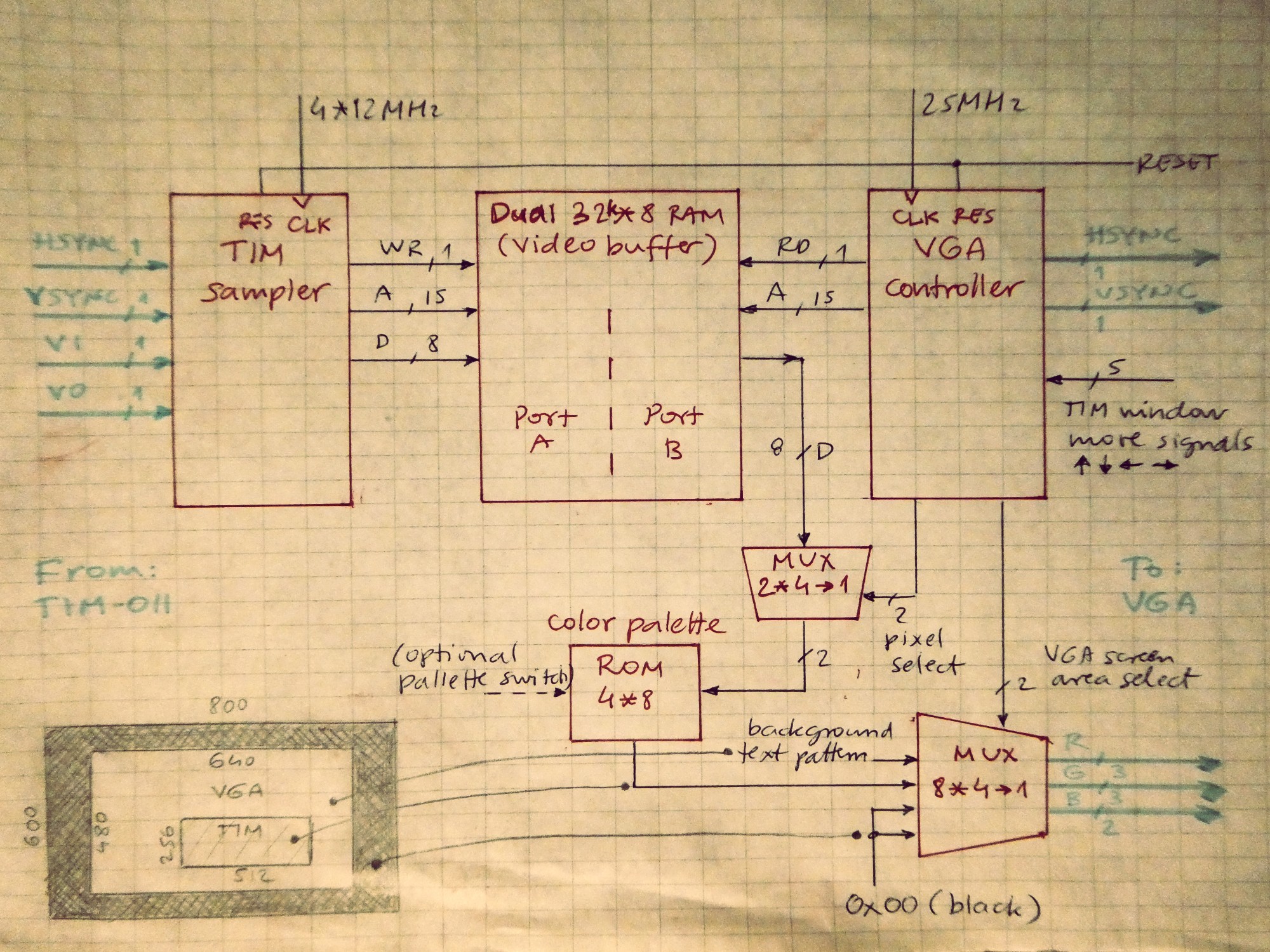
Converting TIM-011 video to VGA
11/29/2020 at 06:14 • 0 commentsConverting incompatible video standards especially in retrocomputing field is a well-known problem, for which a whole cottage industry has been created (e.g. GONBES and similar).
To recap:
TIM-011 VGA (basic mode) Color info Digital, 4 level, 2 signals Analog, 3 signals, theoretically 2^24 colors with 3 8-bit DACs Pixel clock 12MHz 25.125MHz (25Mhz is used for design simplicity) Horizonal sync 15.625kHz 31.25kHz Vertical sync 50Hz 60Hz As can be seen from the above, any simple or "passive" connectivity between the two won't work. The apparent solution is to:
- Capture input signal (synchronized to TIM-011 timing)
- Store video data in memory (buffer)
- Generate output signal from memory (as VGA)
![]() ---------- more ----------
---------- more ----------In the code, the key components behind this are:
As expected, the component input matches TIM-011 signals, and the output the simple RAM interface to be able to write to 32kB RAM:
entity tim_sampler is
    Port ( reset : in  STD_LOGIC;
           clk : in  STD_LOGIC;
           hsync : in  STD_LOGIC;
           vsync : in  STD_LOGIC;
           v2 : in  STD_LOGIC;
           v1 : in  STD_LOGIC;
           a : out  STD_LOGIC_VECTOR (14 downto 0);
           d : out  STD_LOGIC_VECTOR (7 downto 0);
           limit: in STD_LOGIC_VECTOR (5 downto 0);
           we_in: in STD_LOGIC;
           we_out : out  STD_LOGIC);
end tim_sampler;
The clk is multiple of 12MHz to match TIM-011 signals. This can be generated by higher level component using PLL on FPGA, but I simply added a 48MHz external crystal as it is fun to play with them if the board allows.
Critical input to observe is the hsync signal - we know that when it goes from high to low, TIM-011 will start a scan line of 512 dots, each 83.3ns duration (1 / 12MHz). The idea then is to wait for this transition, and when happens, sample the v1 and v2 video inputs with overscan frequency (4 times multiple in this case).
There is some arithmetic behind this:
1 byte to write to RAM == 4 pixels == 16 bits
Therefore, after 16 bits "shifted in" from v1 and v2, the byte has to be written to memory.
In order to make sampling even more effective, it is done both on rising and falling edge of the 48MHz clock, and because FPGAs allow 1 clock per register, effectively there are 3 16 bit registers per video signal one for rising, one for falling and one that combines them:
signal s2, s1, s2r, s2f, s1r, s1f: std_logic_vector(15 downto 0);
signal h: std_logic_vector(10 downto 0);
signal v: std_logic_vector(8 downto 0);
signal sample: std_logic_vector(7 downto 0);
Other signals:
h - goes from 0 to 511, therefore 10 bits are needed because counting can go on until next hsync signal but should not generate RAM write (not sure why I added 1 extra bit?)
v - goes from 0 to 255, but one extra bit as vsync takes time too and count runs
sample - byte to be written to RAM
s2 and s1 are combination of signals captured at clk rising and falling. To experiment, the circuit allows combining them with "or" or "and":
generate_s: for i in 15 downto 0 generate
begin
    s2(i) <= ((not limit(5)) and s2r(i) and s2f(i)) or (limit(5) and (s2r(i) or s2f(i))); --(s2r(i) or s2f(i));
    s1(i) <= ((not limit(5)) and s1r(i) and s1f(i)) or (limit(5) and (s1r(i) or s1f(i))); --(s1r(i) or s1f(i));
end generate;
Note that the for loop is BUILD time, not RUN time (so nothing "runs the loop" on FPGA, but the VDHL synthesis generates circuitry as if s2(15) <= ... s1(15) <= ... lines of code would have been written 32 times.
With this we now have 16 bit s2 signal (captures v2 video) and 16 bit v1 signal. But the RAM byte has 1 bit per each, so we need to convert 16 => 4, generating the "sample".
How is "sample" generated? One has to decide if the video signal was present or not. This is where the "voter" circuit comes in. Based on how many of 4 sample pixels were detected as "1" and the experimentation setting, it returns the vote of "1" or "0" by default:
    with value select vote <=
        '1' when "1111",
        limit(4) when "1110",
        limit(3) when "0111",
        limit(2) when "1100",
        limit(1) when "0110",
        limit(0) when "0011",
        '0' when others;
As there are 8 bits in the "sample" obviously, 8 "voters" are needed, hooked up to right s1, s2 inputs and sample byte bits:
Finally, sample byte needs to be written to RAM:
            case h(3 downto 0) is
                when X"F" =>
                    d <= sample;
                    a <= v(7 downto 0) & h(10 downto 4);
                when X"1" =>
                    we_out <= we_in and (not v(8));
                when X"E" =>
                    we_out <= '0';
                when others =>
                    null;
            end case;
As the h counter runs, we inspect the least significant nibble:
0 ... no operation
1 ... D - write last sample with captured address
E - disable write signal to prevent any overlap glitch
F - capture sample and address to be written in subsequent 16 clock cycle. Note the address schema aligned with TIM-011 video generation hardware described here:
- 128 bytes are used for line 0, then 128 for line 1 etc., meaning that the upper 8 bits of address are "rows" and lower 7 bits are "columns".
As can be seen, the memory write bandwith is pretty low: 48MHz/16 = 12MHz/4 = 3MHz.
Vertical signal processing:
This is simple, at each hsync signal, the vertical count needs to be incremented, and when vsync goes high (one full frame has been captured), it needs to be reset to 0:
on_hsync: process(hsync, reset, vsync)
begin
    if ((vsync or reset) = '1') then
        v <= "000000000";
    else
        if (rising_edge(hsync)) then
            v <= std_logic_vector(unsigned(v) + 1);
        end if;
    end if;
end process;
Note that hsync triggers even after 256 lines, incrementing v. This would cause "good" video info to be overwritten with "no data" as the v counter wraps around. That's why the write logic only work when v(8) == '0', meaning for first 256 lines only. I spent about a week of my life and near nervous breakdown before I found this bug.
VIDEO BUFFER RAM - ram32k8_dualport.vhd
To store 512*256 4 color pixels, 32kBytes of RAM are needed (15 bit address, 8 bit data width). This RAM needs to be:
- written by TIM signal sampler
- read by VGA controller
Given that there are 2 possible approaches:
Single port RAM
The 2 components would need to share a common address, data, control bus in a time multiplexed fashion. Given that we VGA controller needs to generate video signal continuously, it would need the priority to access RAM any time not "drawing off screen" (meaning either hync or vsync are active to simplify a bit). The sampling runs in parallel and continuously, which means that some samples would need to be dropped. This is not really a problem as even moderate speed animations are rather static, perhaps few frames per second, so in the worst case on VGA user would see frame 1 then 4 but not 2 and 3. When image is static (text, graphics), dropped samples would not be perceived at all, simply the circuit would catch up after few 1/50s frame cycles.
Dual port RAM
This is "partial" dual port as 1 port always writes (TIM sampler) and 1 always reads (VGA controller). The FPGA I used has the capacity and "IP" component that does this nicely so I used it:
LIBRARY ieee;
USE ieee.std_logic_1164.ALL;
-- synthesis translate_off
LIBRARY XilinxCoreLib;
-- synthesis translate_on
ENTITY ram32k8_dualport IS
  PORT (
    clka : IN STD_LOGIC;
    ena : IN STD_LOGIC;
    wea : IN STD_LOGIC_VECTOR(0 DOWNTO 0);
    addra : IN STD_LOGIC_VECTOR(14 DOWNTO 0);
    dina : IN STD_LOGIC_VECTOR(7 DOWNTO 0);
    clkb : IN STD_LOGIC;
    addrb : IN STD_LOGIC_VECTOR(14 DOWNTO 0);
    doutb : OUT STD_LOGIC_VECTOR(7 DOWNTO 0)
  );
END ram32k8_dualport;
VGA SIGNAL GENERATION - vga_controller.vhd
There are many different and available VHDL / Verilog implementations of VGA controllers, from the simplest to most complex ones. For the job at hand, I decided to write another one because of some extra requirements:
- custom pixel layout in memory
- conversion of 4 "colors" to VGA colors
- positioning of 512*256 TIM "window" on 640*480 VGA screen
- differentiating when video display info needs to come from "TIM window" (from buffer RAM), or not (area outside of TIM window)
Therefore the component definition is a bit different than expected:
entity vga_controller is
    Port ( reset : in  STD_LOGIC;
           clk : in  STD_LOGIC;
           offsetclk: in STD_LOGIC;
           offsetcmd: in STD_LOGIC_VECTOR(3 downto 0);
           hsync : buffer  STD_LOGIC;
           vsync : out  STD_LOGIC;
           h_valid: buffer STD_LOGIC;
           v_valid: buffer STD_LOGIC;
           h : buffer STD_LOGIC_VECTOR(9 downto 0);
           v : buffer STD_LOGIC_VECTOR(9 downto 0);
           x_valid: out STD_LOGIC;
           y_valid: buffer STD_LOGIC;
           x : out  STD_LOGIC_VECTOR (8 downto 0);
           y : out  STD_LOGIC_VECTOR (7 downto 0));
end vga_controller;
offsetclk, offsetcmd:
allow the TIM window to be moved up/down/left/right within VGA screen. These are hooked up to Mercury baseboard push-buttons and their effect can be seen on the video.
hsync, vsync:
standard VGA sync signals, only 1 mode is supported timing-wise
h_valid, v_valid, h, v:
VGA pixel coordinates and if in valid horizonal and vertical range
x_valid, y_valid, x, y:
TIM pixel coordinates and if in valid horizontal and vertical range
Internally, the registers are updated in two processes, driven by 2 clocks:
1. 25MHz dotclk (lines 116 - 142)
Two key registers updated are:
h_cnt - free incrementing counter with each dotclk (position across the line, but note that includes invisible part of the line too)
h_index - pointer to one entry of the following table:
signal h_signal: signal_lookup := (
    "000000" & std_logic_vector(to_unsigned(95, 10)), -- hsync
    "010000" & std_logic_vector(to_unsigned(47, 10)), -- no signal
    "011010" & std_logic_vector(to_unsigned(63, 10)), -- h_active
    "011100" & std_logic_vector(to_unsigned(511, 10)), -- h_active, x_valid
    "011011" & std_logic_vector(to_unsigned(63, 10)), -- h_active
    "110000" & std_logic_vector(to_unsigned(15, 10)), -- reset at the end
    "110000" & std_logic_vector(to_unsigned(15, 10)), --
    "110000" & std_logic_vector(to_unsigned(15, 10))  --
);
The process starts with h_cnt 0 and h_index 0, and the highlighted "000000" is connected to hsync which is low active. This state goes on until h_cnt hits value of 95, after which h_index increments to 1, and h_cnt is reset to 0, to count towards 47 etc. This is very similar how old washing machine programators worked, pipes and motor actuators are top 6 bits, and lower 10 are time interval measured before kicking into different wet / dry / tumble cycle.
Note the 63 - 511 - 63 pattern - this is how the TIM window is positioned horizontally on the screen, centered with 64 pixels on each side. Obviously, if we could change this to 62 - 511 - 64 that would mean TIM window moved 1 pixel left. This change is the job of the "offset register" component:
h_off: offsetreg Port map (
                reset => reset,
                initval => std_logic_vector(to_unsigned(63, 10)),
                mode => offsetcmd(1 downto 0),
                clk => offclk,
                sel => h_sel,
                outval => h_offset
            );
When looking at the implementation of offsetreg.vhd it is obvious what the "mode" does - push on one button or other increments / decrements the opposite offsets, and pressing both puts them back to initial state (centers the window):
            case mode is
                when "01" =>
                    p_reg <= std_logic_vector(unsigned(p_reg) + 1);
                    n_reg <= std_logic_vector(unsigned(n_reg) - 1);
                when "10" =>
                    p_reg <= std_logic_vector(unsigned(p_reg) - 1);
                    n_reg <= std_logic_vector(unsigned(n_reg) + 1);
                when "11" =>
                    p_reg <= initval;
                    n_reg <= initval;
                when others =>
                    null;
            end case;
There are two registers in the component, p_reg and n_reg which count in opposite direction, as left / right and top / bottom margins are opposite. At the right h_index and v_index, the hard-coded values of margins ("h_current") are replaced with value coming from offset reg (h_offset):
h_limit <= h_offset when (h_reg = '1') else h_current(9 downto 0);2. 31.25kHz vertical (vsync) clock
At end of each horizontal line (per hsync), the vertical counter needs to be updated. The logic and the process is same like for horizontal signal, but the timing constants obviously different:
signal v_signal: signal_lookup := (
    "000000" & std_logic_vector(to_unsigned(1, 10)), -- vsync
    "010000" & std_logic_vector(to_unsigned(32, 10)), -- no signal
    "011010" & std_logic_vector(to_unsigned(111, 10)), -- v_active
    "011100" & std_logic_vector(to_unsigned(255, 10)), -- v_active, y_valid
    "011011" & std_logic_vector(to_unsigned(111, 10)), -- v_active
    "110000" & std_logic_vector(to_unsigned(9, 10)), -- reset at the end
    "110000" & std_logic_vector(to_unsigned(9, 10)), --
    "110000" & std_logic_vector(to_unsigned(9, 10))  --
);
It is obvious that top and bottom margin are now 112 rows (lines) and are being replaced by values coming from vertial offset register. Note highlighted 10 and 11 in the table. 1 on bit position 11 flips the MUX to take the value from offset reg, and 1 on bit 10 controls if the offset reg will serve out "p_reg" or "n_reg".
CONNECTING it all together - sys_tim011_mercury.vhd
Component on the higher level of hierarchy connects the sampler, the RAM, and the VGA controller.
Maybe it is easiest to follow the signals from R, G, B pins backward.
The Mercury base-board has a simple resistor ladder DAC with total resolution of 8 bits, 3 red, 3 green, 2 blue. These bits come from a generate "vga_color" byte
-- now convert to VGA 8-bit color
RED <= vga_color(7 downto 5);
GRN <= vga_color(4 downto 2);
BLU <= vga_color(1 downto 0);
Now remember that an any moment the "electron beam" (or its virtual equivalent on LCD) can only be:
- outside of screen - use color black
- in TIM window - use 1 out of 4 TIM colors as an index into a 4 entry color byte palette
- outside TIM window, but in VGA area - for fun, just generate a text screen background
Like everything else, the above is just a MUX:
-- color index also takes into account selected palette and if in TIM window
color_sel <= vga_window & tim_window;
with color_sel select vga_color <=
    text_color when "10",                                                        -- text outside tim window
    tim_color(to_integer(unsigned(switch(0) & pair))) when "11",    -- tim pixel
    color_black when others;
What is color_sel? Simply a combination of signals from VGA controller indicating in which display window is the "beam":
tim_window <= x_valid and y_valid;
vga_window <= v_valid and h_valid;
The "pair" is actual 2 video bits V1 and V0 stored in the video buffer RAM. These are selected by looking at the lowest 2 bits of the x (horizontal) value the VGA controller outputs:
-- pixels are stored 11003322
-- see https://github.com/zpekic/Sys_TIM-011/blob/master/Img2Tim/Img2Tim/Program.cs
with vga_x(1 downto 0) select pair <=
    vram_douta(5 downto 4) when "00",
    vram_douta(7 downto 6) when "01",
    vram_douta(1 downto 0) when "10",
    vram_douta(3 downto 2) when others;
It is interesting to note how the pixels are stored in a byte - not in an expected way but shuffled around in the nibbles. As the lower 2 bits of x go from 00 to 11, selection of the "pair" needs to follow the storage pattern.
Obviously these bits have to come from vram_douta data port "B" (naming bug!) which is connected to the VGA controller. But where is the RAM address coming from on VGA side?
vga_a <= vga_y & vga_x(8 downto 2);As expected, one "line" (vga_x) is stored in 128 bytes and then there are 256 such lines (blocks of RAM) down the rows (vga_y).
The other RAM port is connected to the sampler, and is write only, when allowed (vram_wea signal generated by sampler):
mem: ram32k8_dualport PORT MAP(
-- sampler only writes
    clka => byteclk,
    ena => '1',
    wea => vram_wea,
    addra => sampler_a,
    dina => vram_dina,
-- vga only reads
    clkb => CLK,
    addrb => vga_a,
    doutb => vram_douta
  );
(small bug: vram_douta should be renamed to vram_doutb)
The actual "tim_color" is a lookup into a small 8 bytes entry ROM. The lower 2 bits are selected by V1 and V0 from buffer RAM (== TIM video signal intensity), and just for fun the upper address bit is connected to switch for instant selection of grayscale or color display:
constant color_black: std_logic_vector(7 downto 0):= "00000000"; constant color_blue: std_logic_vector(7 downto 0):= "00000011"; constant color_green: std_logic_vector(7 downto 0):= "00011100"; constant color_cyan: std_logic_vector(7 downto 0):= "00011111"; constant color_white: std_logic_vector(7 downto 0):= "11111111"; constant color_red: std_logic_vector(7 downto 0):= "11100000"; constant color_yellow: std_logic_vector(7 downto 0):= "11111100"; constant color_ltgray: std_logic_vector(7 downto 0):= "01101101"; constant color_dkgray: std_logic_vector(7 downto 0):= "10010010"; type color_lookup is array (0 to 7) of std_logic_vector(7 downto 0); signal tim_color: color_lookup := ( -- grayscale palette color_black, -- tim pixel 00 color_dkgray, -- tim pixel 01 color_ltgray, -- tim pixel 10 color_white, -- tim pixel 11 -- colorful palette color_black, -- tim pixel 00 color_yellow, -- tim pixel 01 color_cyan, -- tim pixel 10 color_green -- tim pixel 11 ); -
Initializing video memory for test purposes
11/29/2020 at 04:01 • 0 commentsIn order to see if the generated video signal is good or not, one simple trick is to pre-populate video RAM with image as if CPU had generated it.
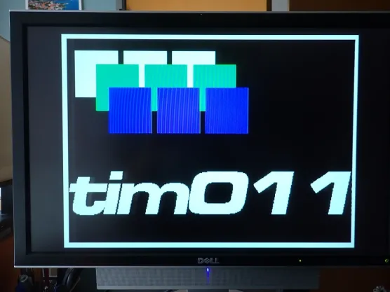
I used two images:
TIM-011 signal generator on Anvyl - my lame MSPaint image:
![]()
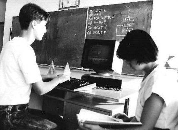
TIM-011 sampler on Mercury - model students busy learning Basic from original 1988 ad (I hope I am not breaking their copyright!)
![]()
Of course, both of these converted to 512*256*4 colors look a bit less impressive...
All FPGAs support initializing RAM/ROM which is part of the design. However, the file format varies. As I was using Xilinx ISE14.7, I needed .coe file to include into project.
Here are steps to generate the .coe:
1. Convert image to .bin file using Img2Tim utility which will:
- Ingest .png, .jpg, .bmp file and instantiate a memory image object from it
- Resize (squish) to 512*256
- Sample the colors using simple thresholds to get only 2 bits per pixel
- Use the knowledge of TIM-011 video memory organization to generate 32kB .bin file
(use Img2Tim.cmd)
2. Once we have the .bin file, use file conversion mode of my microcode compiler to generate .coe from .bin
(use mcc.cmd)
3. Finally, use ISE native tooling to generate the RAM component and point it to .coe file
There are other approaches too - for example, tooling could generate VHDL source code directly that initializes the memory and include that file into the project to be compiled, but such file would be very large and slow down compilation. mcc is able to generate VHDL from .bin file in case non-Xilinx approach is needed.
-
TIM-011 video signal generation ("grafika" component)
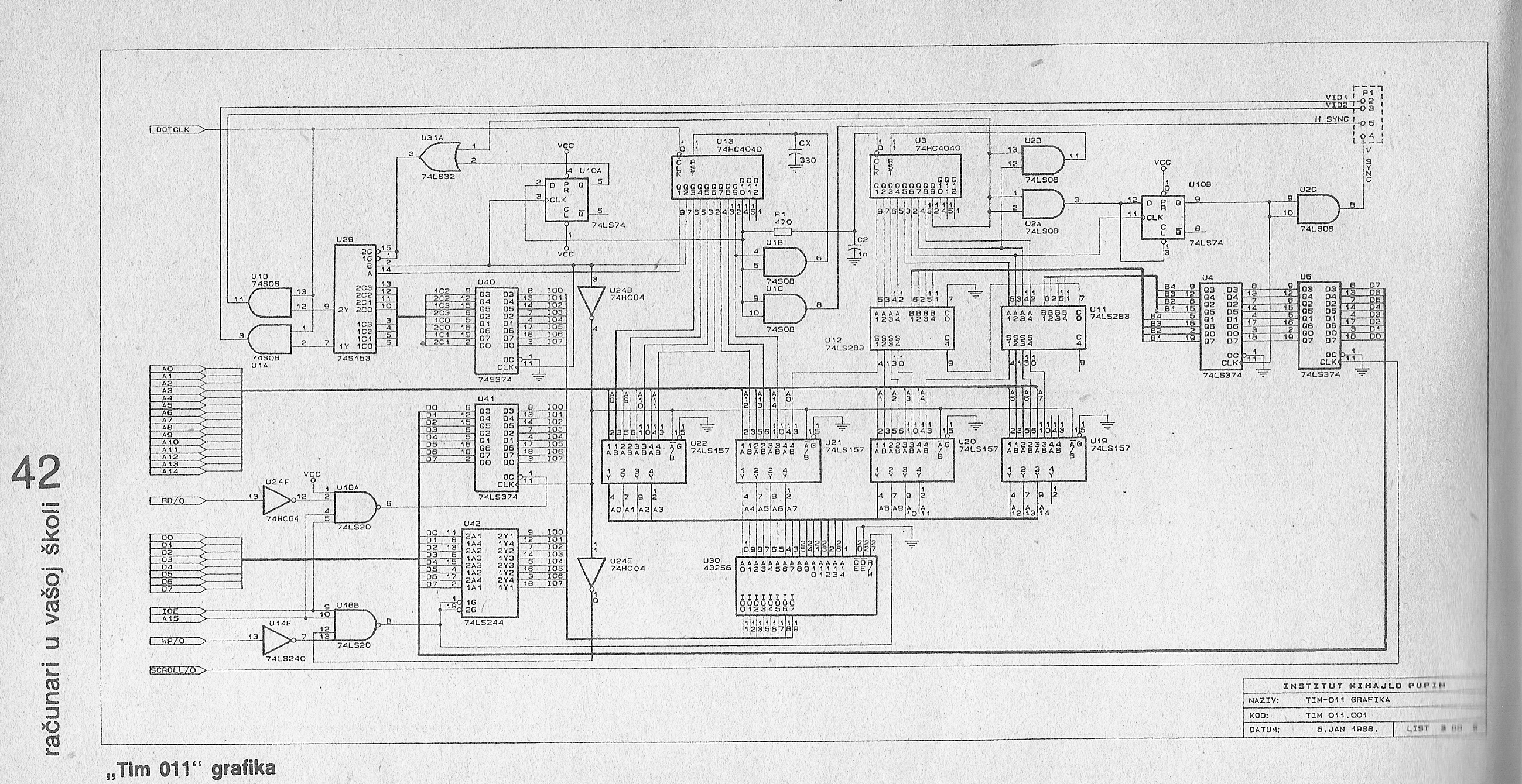
11/29/2020 at 03:35 • 0 commentsIn order to convert video signal coming from TIM-011 to VGA, one has to first have it... As I don't have a TIM-011, I had to "simulate" one. Key component of this simulation is to re-create the custom graphics system of TIM-011 on FPGA.
Luckily, I had the schematics from the magazine, so I could reverse-engineer it.
![]()
First, a bit about TIM-011 graphics implementation:
- Implemented using 74XX TTL and CDXXXX CMOS ICs - no VDP!
- Resolution is 512 (H) * 256 (V)
- Graphics mode only - text is "painted" by software similar to classic Macintosh computer approach of the same era
- 4 "colors" - or shades of gray per pixel. This means 1 byte contains 4 pixels. Total memory needed for picture is then 512*256/4 = 32k
- Video RAM is a single generic 32kB static RAM, it is mapped into I/O space of HD64180 CPU (which has 64k I/O space) from 0x8000 to 0xFFFF
- In addition, simple scroll up/down is supported by varying the offset location of row 0 in video memory.
As a result, following video signal is generated:
- Dot clock is 12MHz
- 1 scan line contains positive HSYC signal, 256 dot periods long (21us), after which 512 dot periods (43us) is the video signal (V2 and V1)
- 1 scan line takes therefore 64us which gives the horizontal frequency of 15.625kHz
- VSYC positive signal comes after every 256 scan lines, and is 2.04ms long (24480 dot clock periods)
- VSYNC repeats at 50Hz, which is the vertical refresh rate (there is no interlacing)
![]()
There are two interesting facts about TIM-011 video:
- V2 and V1 are "anded" with dotclk - this means that their intensity is halved. Not sure why this was done, maybe it improves the image quality on old home computer monitors preventing the pixels to bleed to each other due to phosphorus luminance.
- The pixels are "packed" in a byte in a strange way:
Bit: 7 6 5 4 3 2 1 0 Pixel: 1 0 3 2 Intensity: V2 V1 V2 V1 V2 V1 V2 V1 VDHL implemenation:
To follow description below, refer to this source code file.
(to be updated)
-
Demo video
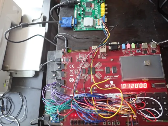
11/29/2020 at 02:21 • 0 commentsReally low-quality, terrible video, but hopefully illustrating what is working so far:
Anvl-board generates video signal:
- Converted to CSYNC (composite sync) + RGB digital, goes to GBS8200 board towards VGA
- Raw (HSYNC+CSYNC+V2+V1) goes to Mercury board
- Scroll up/down is supported like real TIM
- Test signal mode has been added, it displays a 4 color box pattern
Mercury board captures the video signal:
- Incoming video signal is converted to memory bytes and stored in 32kB onboard RAM
- VGA controller reads the same RAM, applies a 4-color palette and outputs as 640*480, 60Hz
- Display outside TIM-011 512*256 window is filled with hard-coded ASCII characters (text display in the future)
- TIM window can be moved on VGA screen (it is centered initially)
Upcoming project logs will describe these in more details.
TIM-011: FPGA-based VGA and PS/2 keyboard adapter
Trying to connect vintage TIM-011 home computer with PS/2 keyboard and VGA using a FPGA developer board