-
Rev 2 PCB, TMDS and SERDES working
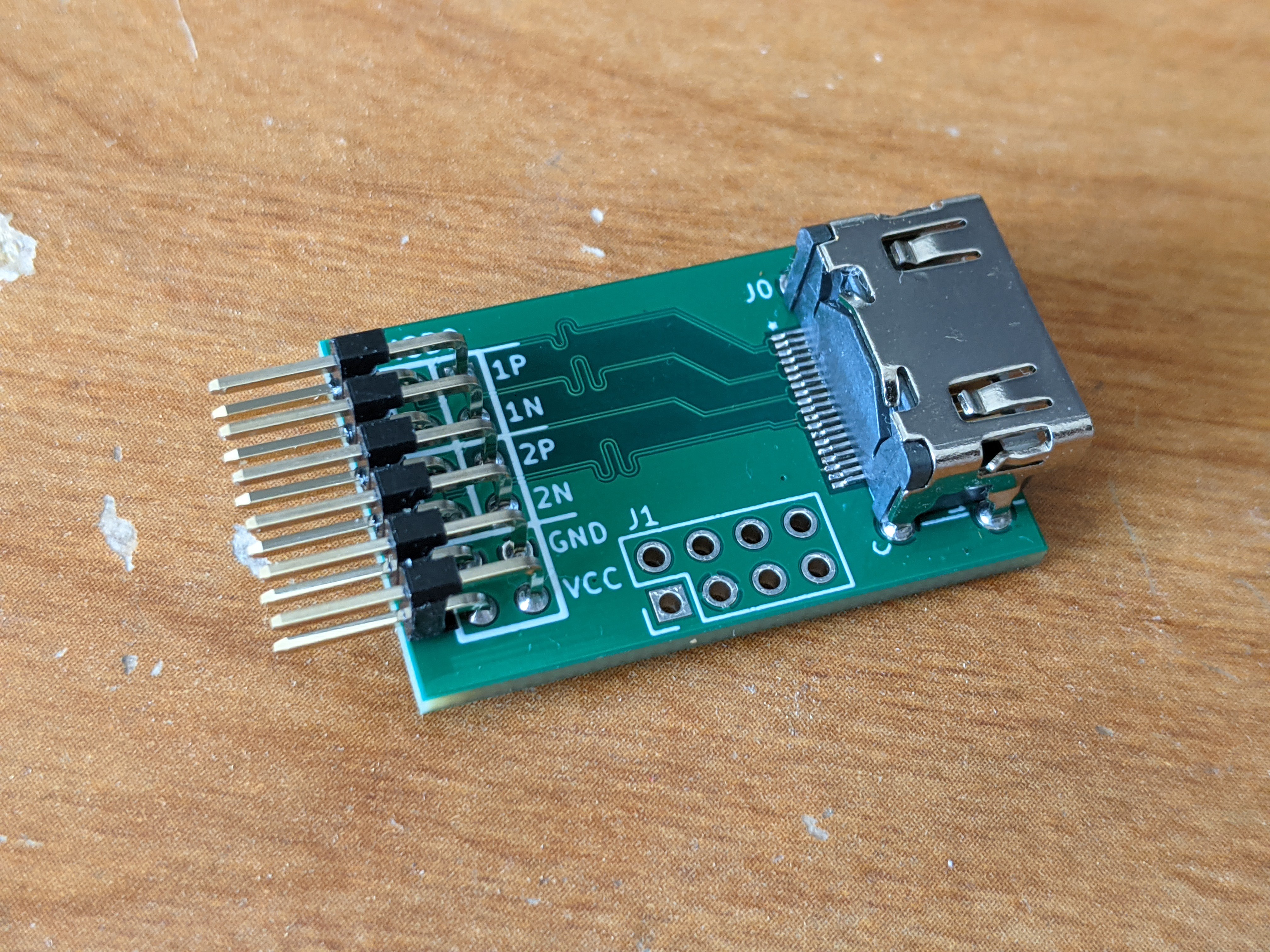
04/27/2021 at 22:38 • 0 commentsOops... PCB v2
Shortly after my last post, I did a quick connectivity check, and I found that I screwed up the HDMI connector footprint! The pin numbers ended up being reversed from what they should have been. I'm not sure whether I did that, or if I downloaded the footprint that way, but shame on me for not double checking.
After fixing the footprint, I reordered and reassembled the board. Much better now!
![]()
For those curious, I tested this by hooking up an HDMI to DVI cable, and then checking with an ohmmeter. I compared the actual pinout with a diagram for DVI.
Setting up TMDS IO and SERDES
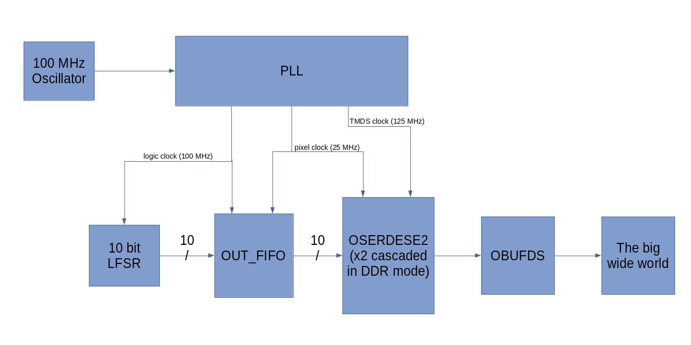
Before this, I had never directly instantiated any of the Xilinx primitives or done any advanced IO stuff away from work, so I wanted a way to test it separately from the display logic. To do this, I made a project that sets up the clocks with a PLL, a SERDES module for serializing the data, and an output buffer. I also made a linear feedback shift register to generate a pseudo-random sequence of 10-bit integers. An OUT_FIFO module is also present to separate the pixel clock domain from a potential logic clock domain in future designs.
![]()
The result is a random bit pattern clocked out at 250 megabits/s (twice the 125 MHz TMDS clock, since the OSERDES modules are configured in DDR mode). I recently purchased an SDS2352X-E oscilloscope from Siglent to measure precisely this type of signal. With a bandwidth of 350 MHz, we're able to capture the fundamental at 125 MHz loud and clear, and probably around 80% of the third harmonic at 375 MHz. On top of that, it has optional 50 Ohm inputs, which is essential when making DIY probes for high-speed stuff. For around $850 brand-new, it's the best budget high-speed scope I could find without trolling eBay.
Nothing works the first try
This being such a simple design, I thought I could get away without simulating it. That, however, quickly proved to be wrong. I loaded a bitstream onto my board, hooked up the scope, and... nothing. Normally I would pull out Verilator at this point, but this design directly instantiates Xilinx primitives that Verilator has no model for. To get around this, I used xsim, which is the simulator that comes bundled with Vivado. Lucky for me, FuseSoC/Edalize has an xsim backend, which makes using it as easy as adding a couple lines to my core config file. I think I could potentially compile some of the models for Verilator but using xsim was definitely the path of least resistance here.
Once setting up xsim, I ran the simulation. The results surprised me to say the least. Everything seemed to work just fine! The clocks were running, the SERDES module was serializing, and the differential outputs were swinging. As frustrating as this was, it narrowed down the problem to some sort of inconsistency between my dev board PCB and my design.
Sure enough, this was it. My scope can only terminate to ground, so I had configured the design for 2.5V LVDS instead of 3.3V TMDS, which requires pullup resistors to 3.3V. The IO bank for this PMOD, though, is hardwired for 3.3V. This means the 2.5V configuration was probably putting the IO bank into an over-voltage protection mode! Switching the configuration to 3.3V TMDS and terminating to 3.3V fixed the problem.
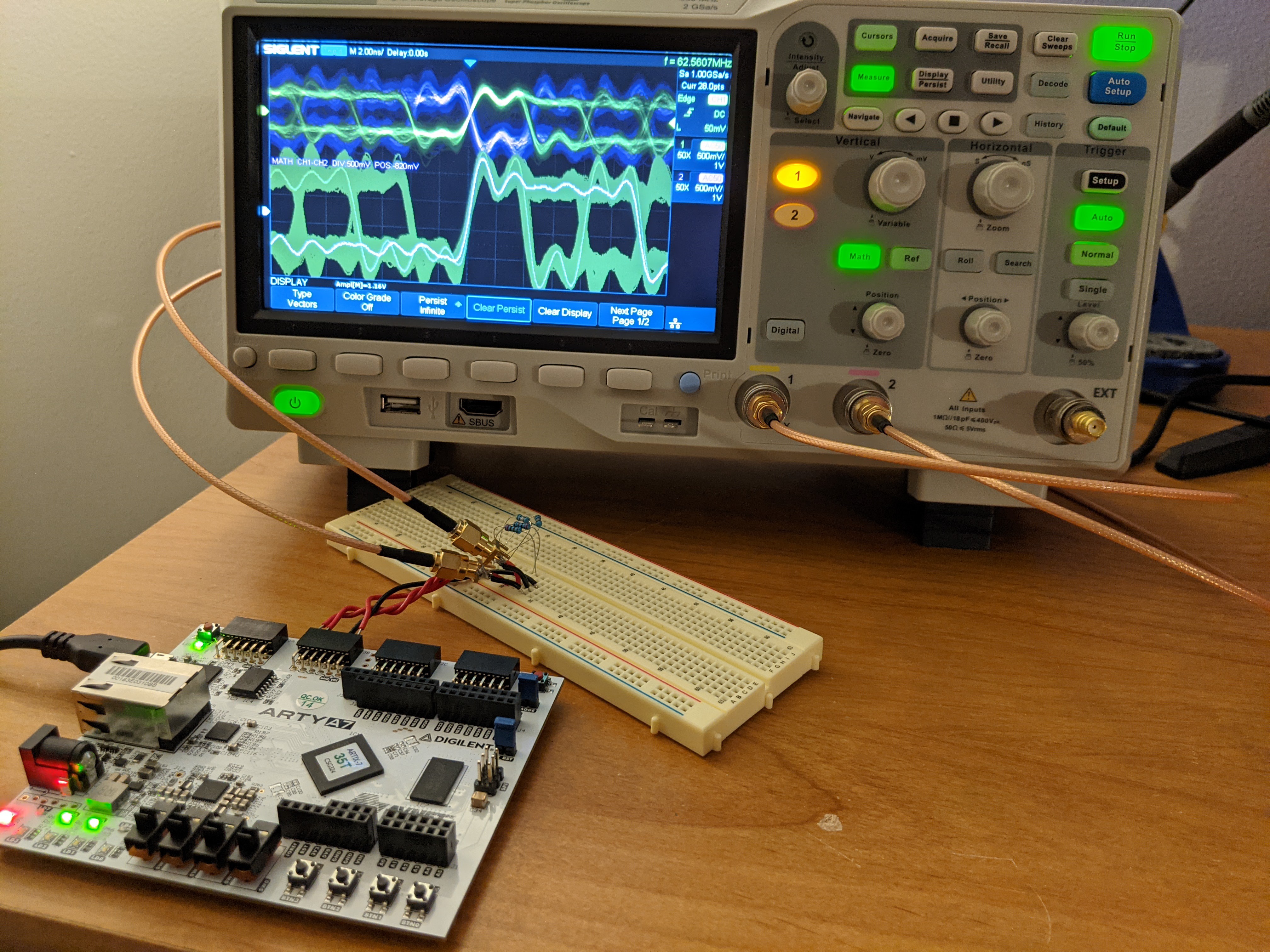
Test setup
Here's an image to do the talking for me.
![]()
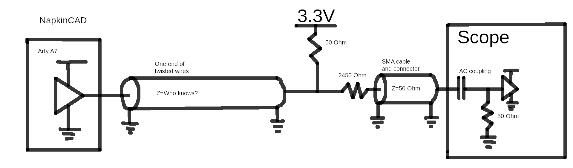
The circuit diagram for a single end of the differential pair is pictured below. If I were using LVDS, I could have hooked up the SMA cable and connector directly to the PMOD interface, but TMDS termination requires that I have a high impedance between my scope and the circuit under test. I picked a 2450 Ohm resistor because it gives an attenuation close to 50:1, which is one of the options that my scope lets me select. In reality though, the resistor I had available was closer to 2.2 kOhm, which gives an attenuation of 45:1.
If you have never used one of these transmission line probes before, they are surprisingly high bandwidth at the expense of loading down your circuit more than the typical 10 Meg passive probe. They do require a 50 Ohm input on your scope, however.
![]()
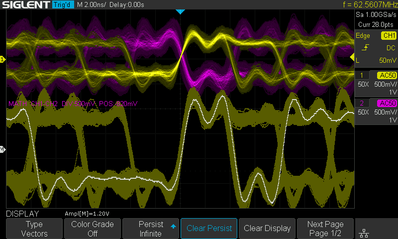
Test Results
If I had $100K to burn on a 20 GHz scope, I'm sure you would see some nasty reflections along the edge; however, with a -3 dB bandwidth of 350 MHz, the waveform looks mighty fine for some through-hole resistors on a breadboard. Since I don't have a differential probe, I connect each end of the differential pair into a separate channel on the scope. Then, I use the math function to subtract them. With the hodge-podge breadboard setup, there was quite a bit of noise common to both ends of the pair, which gets cancelled out nicely when you find the difference between them.
Keen readers may also notice that this is not a true eye diagram. To get an actual eye diagram, you also need a reference clock. When you trigger on the edge of your data signal in infinite persistence mode, all of the edges will line up neatly right in the center of the screen. In reality though, the receiving device needs to generate a clock signal so that it knows where the center of the bit is. The frequency of the data signal may vary from this generated clock in a phenomenon known as jitter, which will cause the edges to not line up so neatly. Fancy scopes from big-name vendors will include software to generate this reference clock post-capture, and then generate an eye diagram. Alternatively, you can also probe the clock signal and trigger on that. The nice thing about this scope is that it has a long record length of 28 megapoints, which makes it possible to generate reference clock, should I choose to write the software to do so. It also has an external trigger input for a clock signal should I need to go that route in the future.
![]()
Final Thoughts
The next step is to generate actual images! There is plenty of code online to do so, so hopefully my next post will be soon. Additionally, I plan to not get sidetracked. Between the last two post I worked on a different project writing a FuseSoC core for the Digilent PMOD AD1.
-
PCBs Assembled
01/23/2021 at 22:37 • 0 commentsPCB Assembly
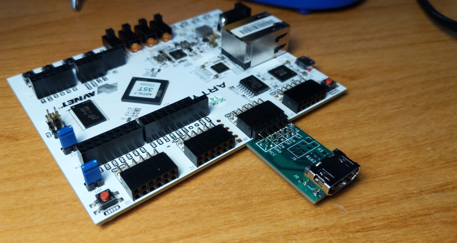
The PCBs that I ordered came in this week, and they look nice! I am surprised at how tiny they feel compared to how they looked on my monitor. An assembled PCB plugged into my Arty A7 board is shown below. I didn't solder the header or resistors connected to the sideband signals, since I'm not planning on using those yet.
![]()
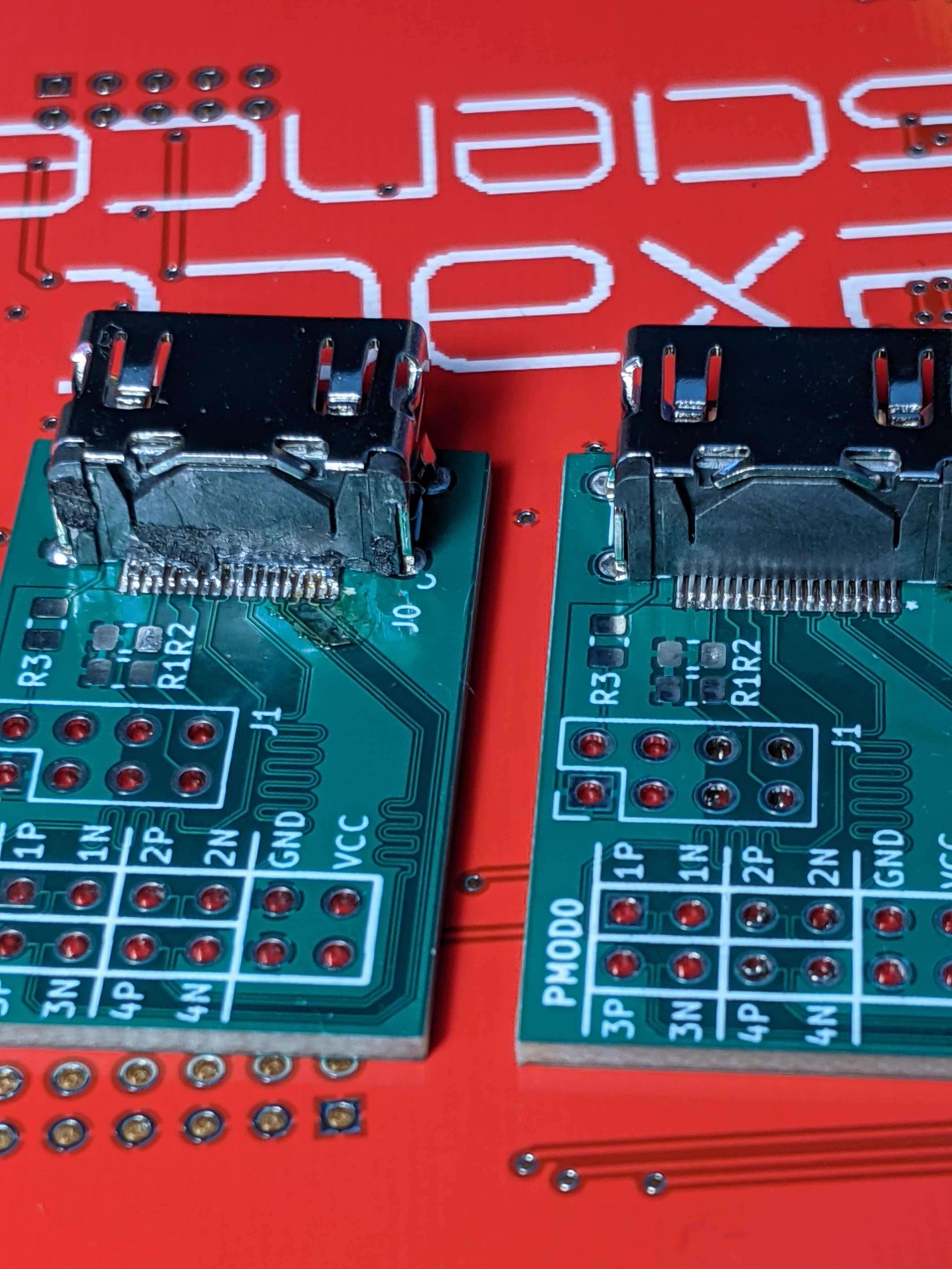
Admittedly it took me two attempts to get the HDMI connector soldered down correctly. I have a Hakko FX-888D iron which works well enough, but a hot air station and some solder paste would have definitely helped with the 0.5 mm pitch pins on the HDMI connector. I tried doing it the quick and dirty way the first time around by swiping across all of the pins, and then cleaning up with some solder wick. You can see how well that turned out below.
![]()
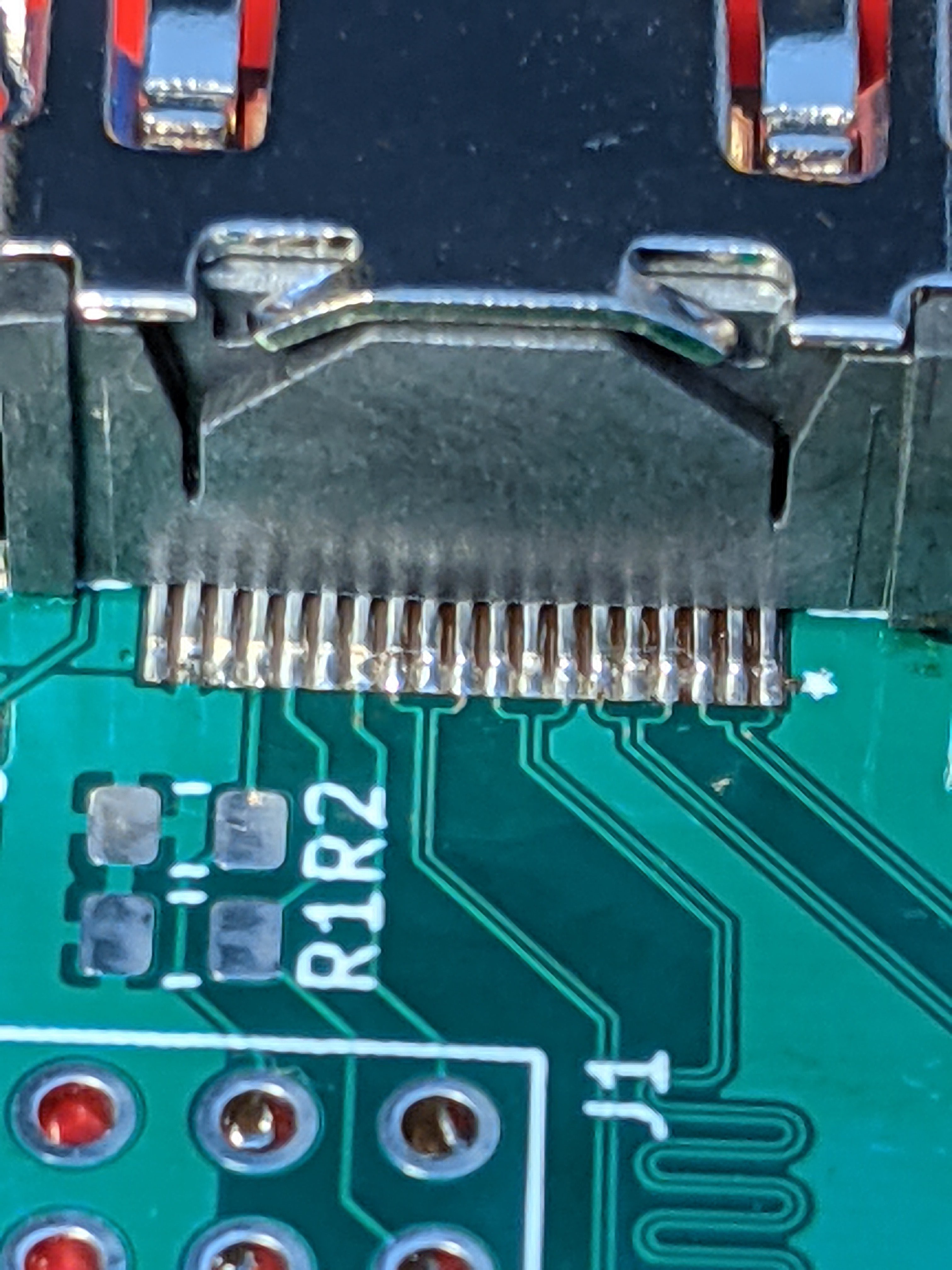
On my second attempt I applied some flux to each pin, and then hit each one individually with a tinned iron. This still required some cleanup with the solder wick, but the result is much prettier. Here's a closeup.
![]()
OpenEMS Simulation Progress
I did spend a weekend trying to import the PCB into OpenEMS, but ran into some problems with the tools I tried. I first tried pcbmodelgen, which converts Kicad PCBs into an Octave/Matlab description of the geometry the mesh needed for simulation. While the examples worked fine for me, I couldn't figure out how to make it work with four layer boards. Next I tried pcb-rnd. It has a plugin for reading Kicad PCBs, but I think the version of Kicad I am using is too new for it. Upon importing my PCB, it puked with a message about the file format being unrecognized.
For Gentoo users, I created ebuilds for both pcbmodelgen and pcb-rnd, which you can access here and here. The pcb-rnd ebuild is pretty lazy, and could have been done better had I taken the time to learn the project's replacement for autotools.
I still plan to do a simulation at some point, but it will require some more work. I think the route forward will require that I either make changes to pcbmodelgen or roll my own tool. Whichever way I choose will probably warrant its own post, so stay tuned here for any updates.
Next Steps
Testing the PCB is the next thing in the queue for me. I'm hoping I can simply load up the project from Domipheus Labs and hit go. Once that's done, I will work on writing my own module in Verilog and packaging it up with FuseSoC.
-
Layout complete
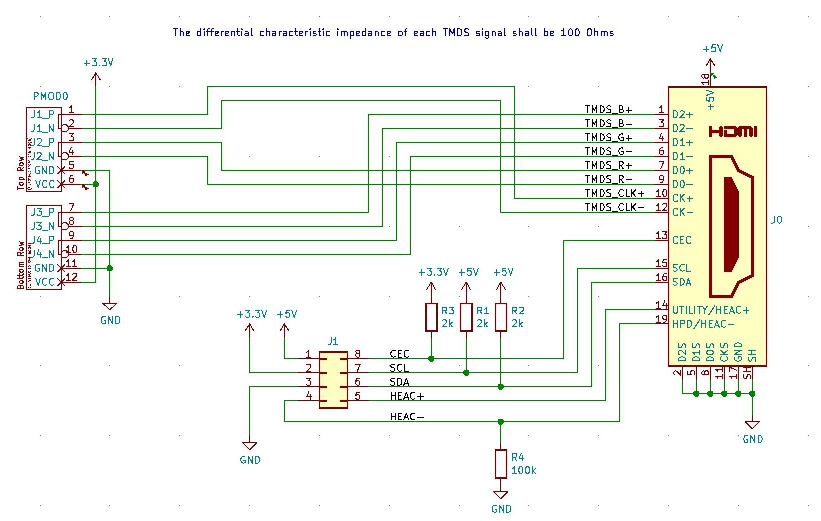
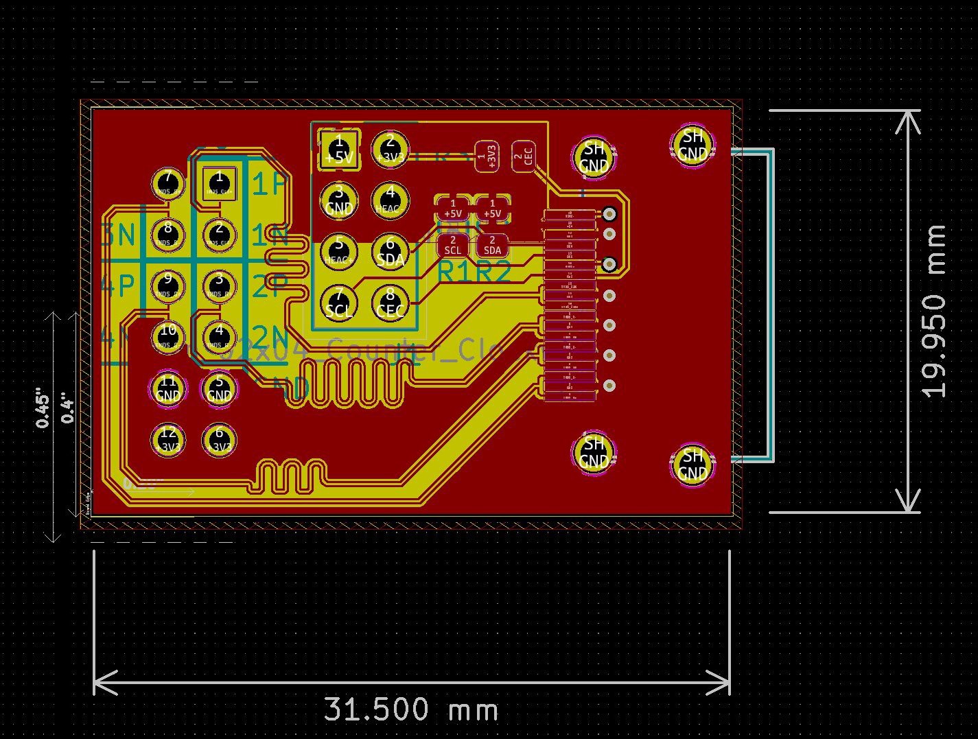
12/21/2020 at 04:39 • 0 commentsI started doing layout with JLCPCB's 2-layer stackup, but I quickly realized that I wasn't going to be able to hit 100 ohm differential mode characteristic impedance with such a thick dielectric. Lucky for me, JLCPCB offers 4-layer boards for just a couple more dollars. They offer two separate 4 layer stackups: JLC7628 and JLC2313. I went with JLC2313 since the thinner dielectric shrinks your trace width when controlling the impedance.
I also made a couple changes to the schematic, including swizzling around the TMDS pairs to make routing easier, and adding in some missing pull-ups and pull-downs.
I have also been playing around with the OpenEMS 3D field solver in my spare time, and I would really like to plug this board into it and see how well it holds up. I used JLCPCB's calculator for choosing track width and spacing, and I am curious how accurate it is. I might potentially create some S-parameters for the board as well, but we'll see.
![]()
![]()
HDMI PMOD
An HDMI breakout board for the high-speed PMOD slots on the Arty A7 35T