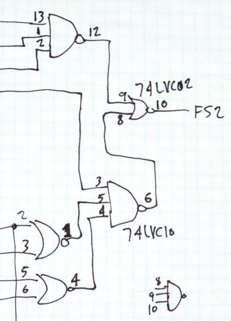
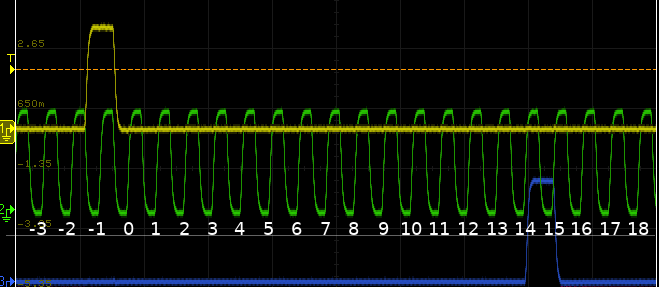
I woke up thinking that I never actually verified the frame sync pulse was really in the correct position in the 256 bit frame. It's not like Verilog or anything else reliable created this circuit... just me doodling NAND & NOR gates on graph paper.

(plus me connecting them right in the PCB layout without any sort of CAD schematic, but as you can see, I did write in the pin numbers on the paper as I chose each gate's pin to use in the layout)
So I loaded the image in Gimp and added text for each rising edge's bit number.

That's a minor relief.
But I'm still a little worried about hold time. I probably need to get out a CS42448 board and look at whether Teensy and the CS42448 are updating their data outputs on the rising or falling edge of BCLK.
 Paul Stoffregen
Discussions
Become a Hackaday.io Member
Create an account to leave a comment. Already have an account? Log In.