TX8 Specifications:
- 65C02 @ 2MHz CPU, 4MHz possible with a few updates
- 32KByte ROM (Flash memory)
- 128KByte RAM (SRAM)
- 2 RS232 serial ports
- 2 Joystick Ports (With real analog input)
- External I2C Port
- YM2149F and SID (either 6581 or 8580) sound chips
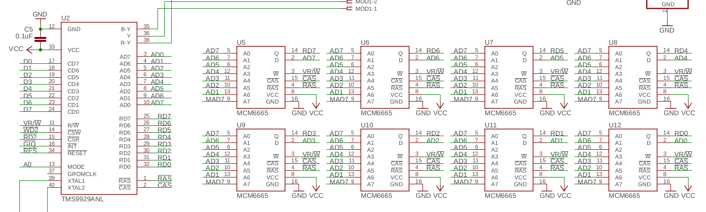
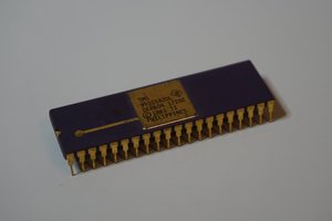
- TMS9929A graphics controller with TMS-RGB video encoder
- 32 KByte Graphics memory bank switched
- Internal W65C22 keyboard controller
- Compact Flash Card slot
Address map
The computer makes use of the entire addressable area that the
6502 processor provides.

                 |-------------|
                 |    FLASH    |  256 byte
                 |-------------|
                 |     IO      |  256 byte
                 |-------------|
                 |             |
                 |    FLASH    |  15872 bytes FLASH
                 |             |
                 |-------------|
                 |             |
                 |   16KByte   |
                 |    banked   |  16384 bytes RAM
                 |     RAM     |
                 |             |
                 |-------------|
                 |             |
                 |             |
                 |             |
                 |             |
                 |   32Kbyte   |  32768 bytes RAM
                 |     RAM     |
                 |             |
                 |             |
                 |             |
                 |             |
                 |-------------|


RAM
The computer is designed to take up to 128Kbyte of RAM using a
monolithic 128Kbyte device. The lower 32Kbyte (0000 - 7FFF) is a
contiguous block. The following 16Kbyte area (8000 - BFFF) is a
windowed (banked) area where any 16K boundary memory chunk from
the available memory can be mapped in. 4 bank select bits are used
to select the bank the user wants to have access to.

The first 64 Kbyte of the 128Kbyte is linerly mapped to the 64K
memory area of the 6502. All accesses between 8000 up to BFFF will
create a banked access. A banked access will map the bank select
bits onto addresses A14-A18 instead of the regular address bus thus
creating an access to the selected bank. Note that the entire
memory can be selected, including the parts that is in regulate
memory space (0000-7FFF, C000-FFFF).

FLASH
The system also contains a small flash memory (16KB) that should be
used be used for early boot. This memory can be disabled allowing
the system to access the RAM that is available from C000-FFFF.

The signal SHDW (Bit 6 on the output port of the SCN2681) is used
to enable or disable the ROM/FLASH memory. The output pin is set to
1 (logic high) after reset and should be set to 0 to disable the
ROM memory. The design idea was that when the ROM is enabled, the
RAM at the same address can still be written to which would enable
the user to copy the content the ROM

I/O Space
256 bytes is allocated for hardware peripherals (I/O). This area is
located from FE00 - FEFF.

  Address range size Description
  * FE00 - FE0F  16  W65C22 keyboard controller.
  * FE10 - FE1F  16  SCN2681 Dual UART controller.
  * FE20 - FE2F  16  PCF8584 I2C controller.
  * FE30 - FE3F  16  YM2149 Audio controller.
  * FE40 - FE5F  32  SID6581 Audio controller.
  * FE60 - FE5F  16  TMS9929ANL Graphic controller.
  * FE70 - FE6F  16  ADC0801 Analog to digital converter.
  * FE80 - FE7F  16  Compact Flash / IDE controller.
  * FE90 - FE9F  16  RTC72421 Real time clock
  * FEA0 - FEFF  96  Experimental I/O

BIOS
The BIOS provides the system with basic input, output and graphic
functionality. 128 call vectors are defined in ROM located from
FF00 up to FFFF. The top three vectors are the processor NMI,
RESET and IRQ vector and the rest are BIOS function calls.

A call to the BIOS is done with the following instructions:

BIOS_CALL:  JMP ($FF00, X)    ; This function will call the BIOS
                              ; pointed to by the the X register.

The user will then use the following instructions to call the BIOS.

            LDX #BIOS_GETCHAR
            JSR BIOS_CALL

* Notice this uses 65C02 specific instructions so this will not
work on older 6502 NMOS processors.
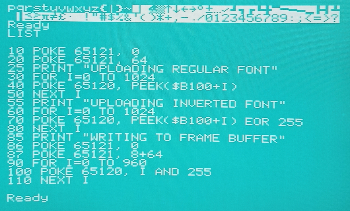
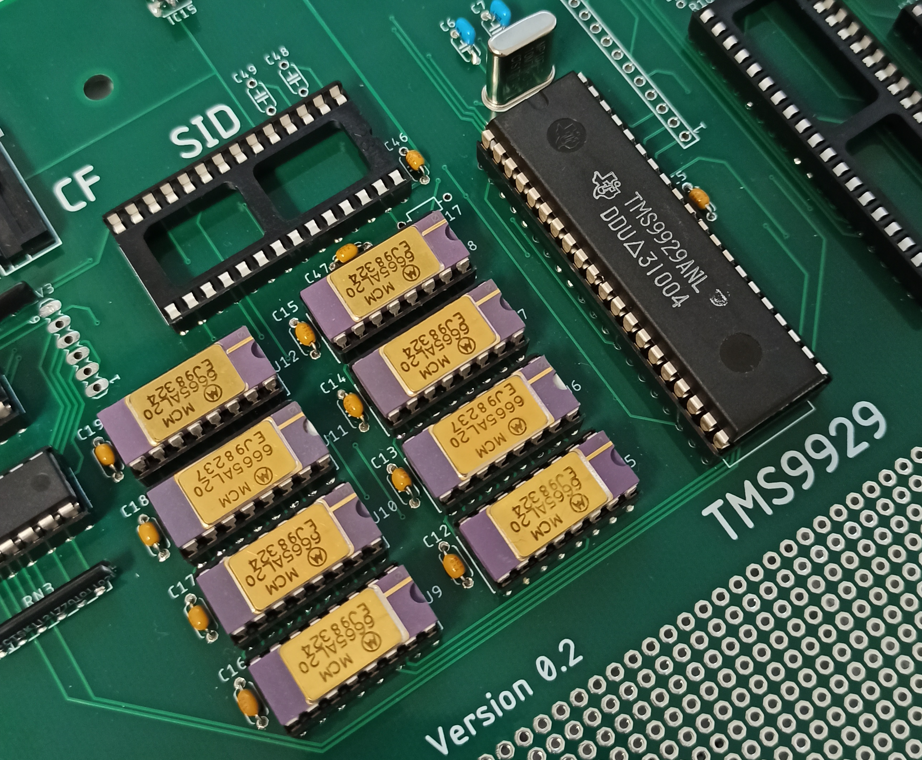 Second stage of the testing was to install the DRAM's and make sure that I can write data and read it back properly. So I wrote a short test program that wrote a test pattern to the memory and verified that it would read back properly. I let the program run for a few hours and no errors were found during this time. I also verified all the setup and hold time parameters with an oscilloscope, just to put my mind at ease. The VDP seem to perform significantly better than specified which means the timing margins are very good.
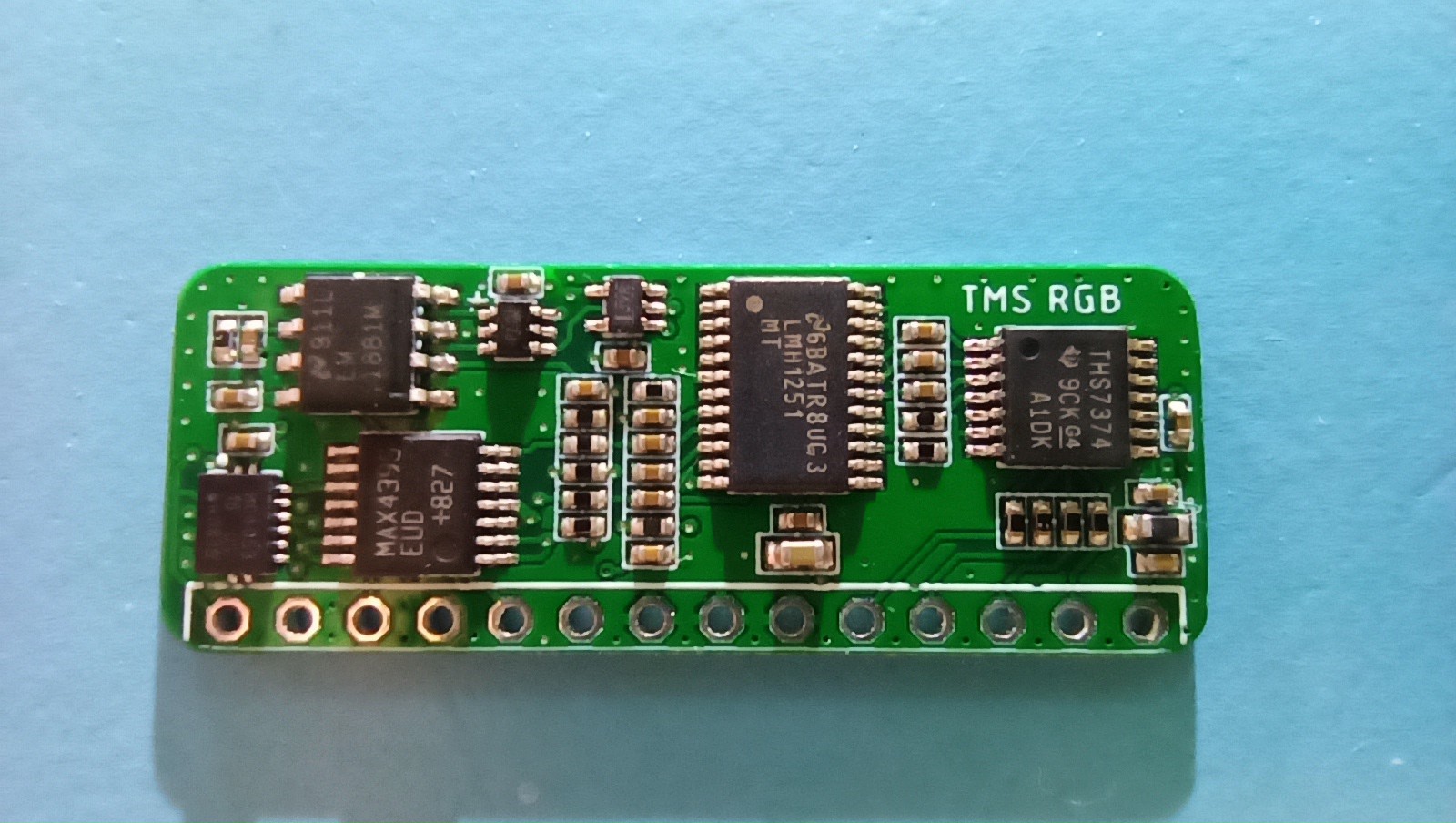
 Erik Piehl
 Clyde Shaffer
 Anders Nielsen