techknight
-
Deciphering the PAL Logic
03/11/2021 at 00:15 • 1 commentOnce all of the dumps of all the PALs are obtained, thats when things get interesting. We have to turn those dumps into logic diagrams.
At this point, I began searching around on the internet to see if there were any projects that could decode the "dumps" back into the logic that I needed to help demystify the architecture of the system. Mainly, the memory map.
I decided to go with this project here:
https://github.com/psurply/ReGAL
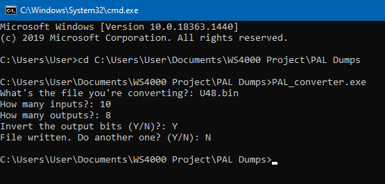
In order to get the logic out of the dump, I have to convert it into a format that this program/script can understand. That's where I had a friend of mine make a utility to do this in C# as I was busy with other things and he wanted to help contribute.
There were a few bugs that needed worked out, But.... the tool work pretty well. you could specify the file, number of inputs, and then number of outputs. However, the tool still has a few bugs where it doesn't put a comma where its needed, and it orders the signal names wrong. But that's not a big deal, I just have to remember that I have to swap those around when it generates the CSV file.
![]()
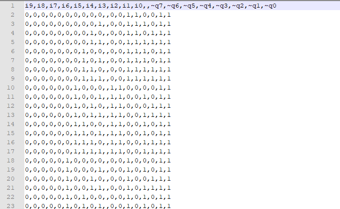
Eventually, you end up with something like this:
![]()
This represents the CSV file that the ReGAL python scripts require to be able to generate the verilog output.
But, as you can see, we still have a layer of obfuscation that we need to work through. And that is the signal names. only thing it knows is i0-ix, and Q0, through Qx.
What we have to do at this point is basically rename the signals in the csv file to ones that actually make sense. And the only way to do this is by looking at the schematic, and attempt to make educated guesses based on the circuit design, and how the PAL is used. Takes pretty good critical thinking skills here.
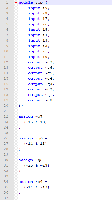
Otherwise if you don't perform this step, you end up with this after you run the script:
![]()
Not very helpful, unless you wanna do this the hard way, of course. :-)
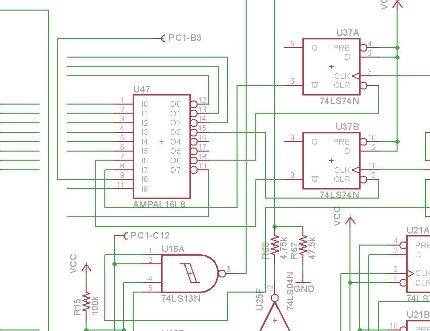
So, back to the schematic to see what we can decipher. There are plenty of things here we can take out of the equation that are known constants. For example, the CPU itself:
![]()
We know what all those signals are on the 68K CPU. so we can define all those net values.
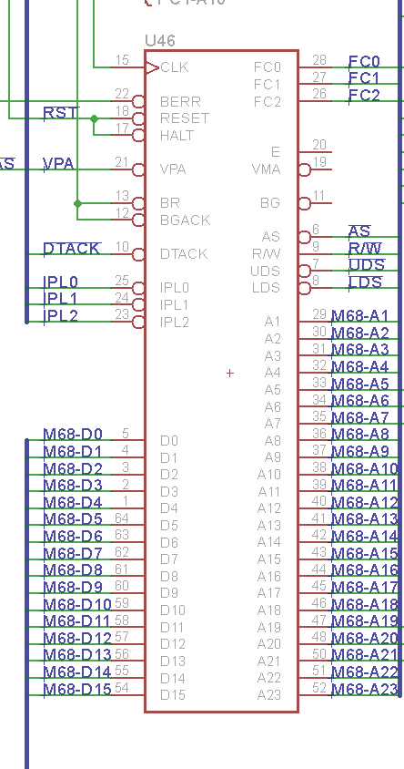
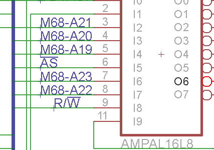
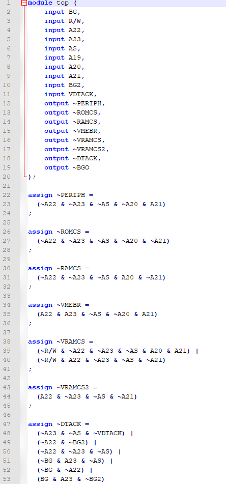
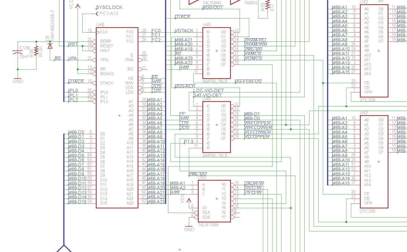
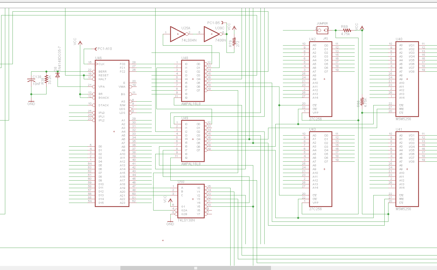
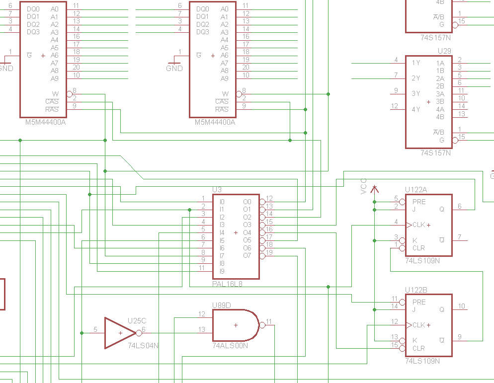
For the sake of this discussion, Lets pick U48 which is an AMPAL16L8. Lets see if any of these signals match up into what is connected into U48:
![]()
Here we go. the majority of the inputs are connected into the CPU Bus. So we can go ahead and name those nets in the CSV file going into ReGAL. we can also see the R/W line connected, as well as the Address Strobe and some address lines. So this chip does address decoding. We can safely make this assumption.
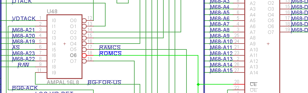
Next thing is to look at what other chips are hooked into that PAL, especially on the outputs:
![]()
Ah! we see that the ROMs are connected into this IC. So we know for certain that this is an address decoding PAL, which will be critical to figure out for deciphering the architecture.
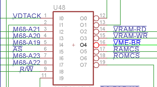
Wash... Rinse... Repeat. Given known facts that its VMEBus, and where else traces are connected, you can figure it out. Eventually, I end up with this:
![]()
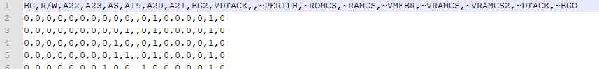
Perfect! One chip down. So, we can go ahead and rename our signals in the CSV file for processing.
![]()
That's better! At least this will make the logic much easier to understand. Now, it is time to run it through the ReGAL script.
![]()
Bingo! Now, isn't that easier to read and figure out? I think so. Now, it is just a matter of going through each and every PAL and do these steps.
Note: There will be signal names that you just don't know what they are doing. And I still have that. But it is what it is. We can make educated best guesses here and still get what we need.
Eventually it starts to look more complete: (prepare to spend many more hours, as I did)
![]()
-
Dumping the PALs
03/10/2021 at 01:49 • 0 commentsSo the next battle in the journey is figuring out how to dump the PALs. So I did alot of googling and research.
With combinational-only PALs, you can easily dump them like a ROM. but you have to know the inputs/vs/outputs. Luckily by looking at the schematic, its pretty straight forward to do so.
But just dumping them as PROMs are only half the battle. You still have to figure out some way to reverse it back into logic.
Every little PAL project I ran into, had its own way and method of reading chips. Plus, I didn't have any of the hardware that was necessary to dump a PAL to run through one of these programs.
So, what I did was take a blend. of my own tools, and online tools.
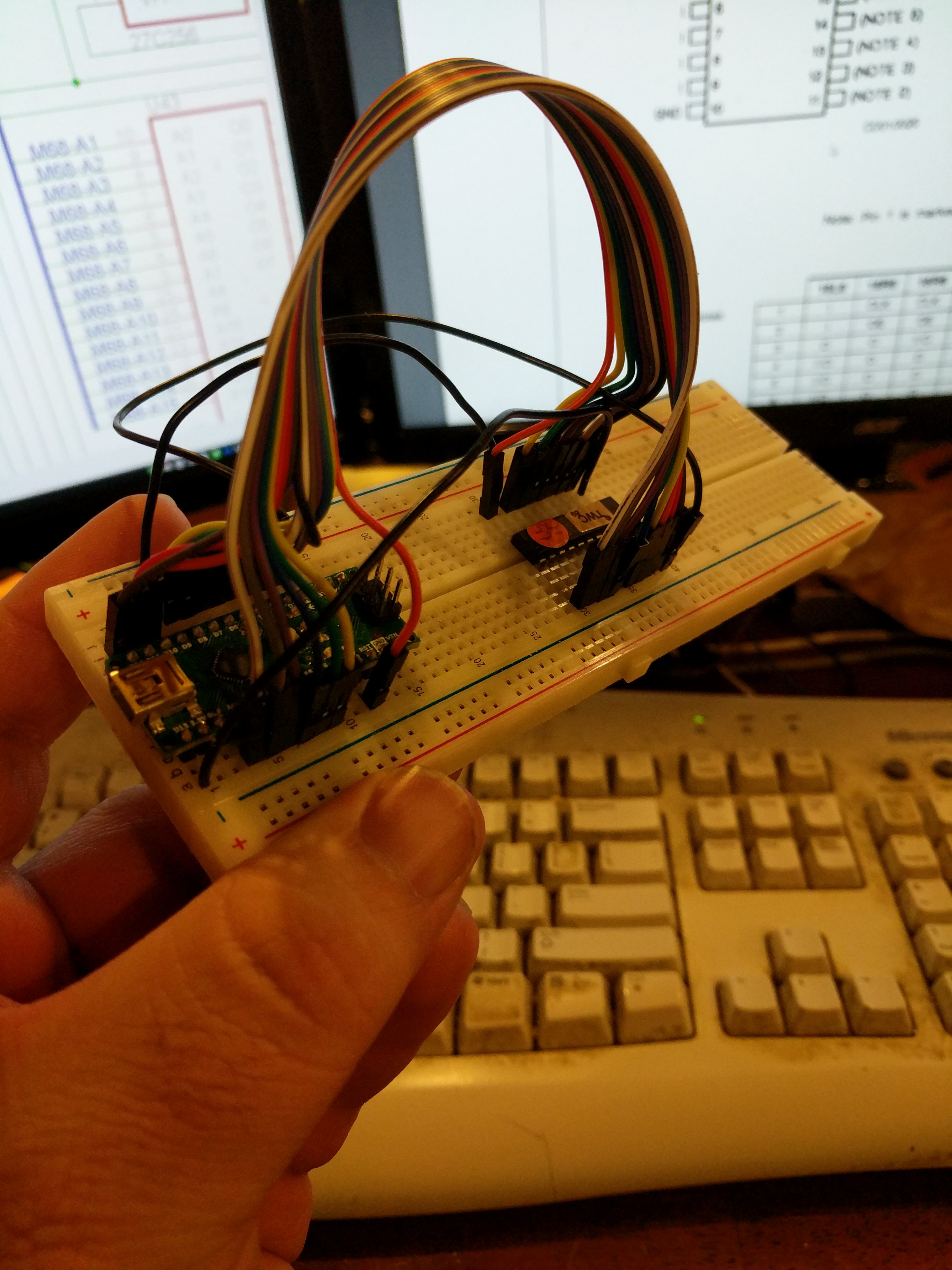
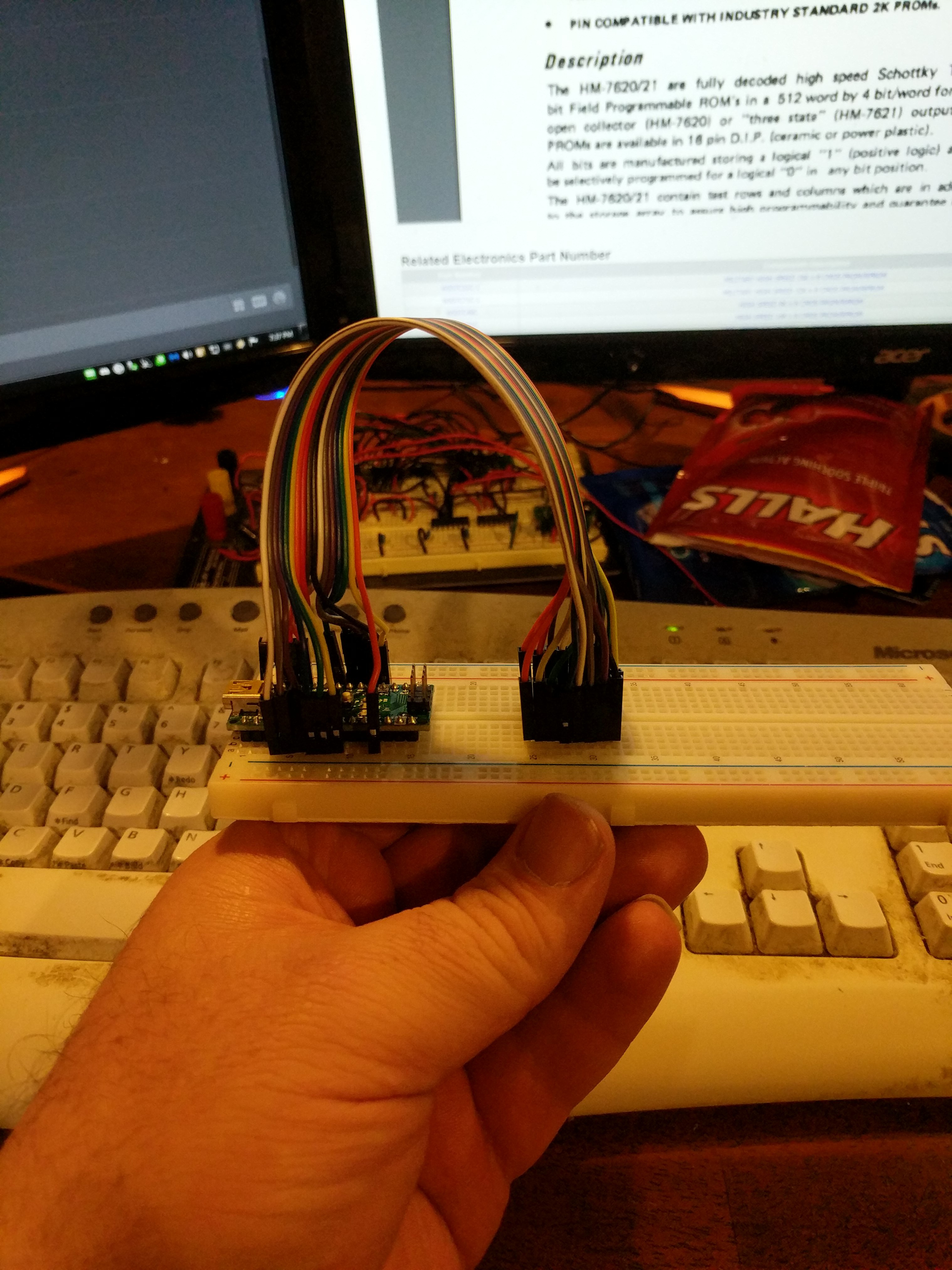
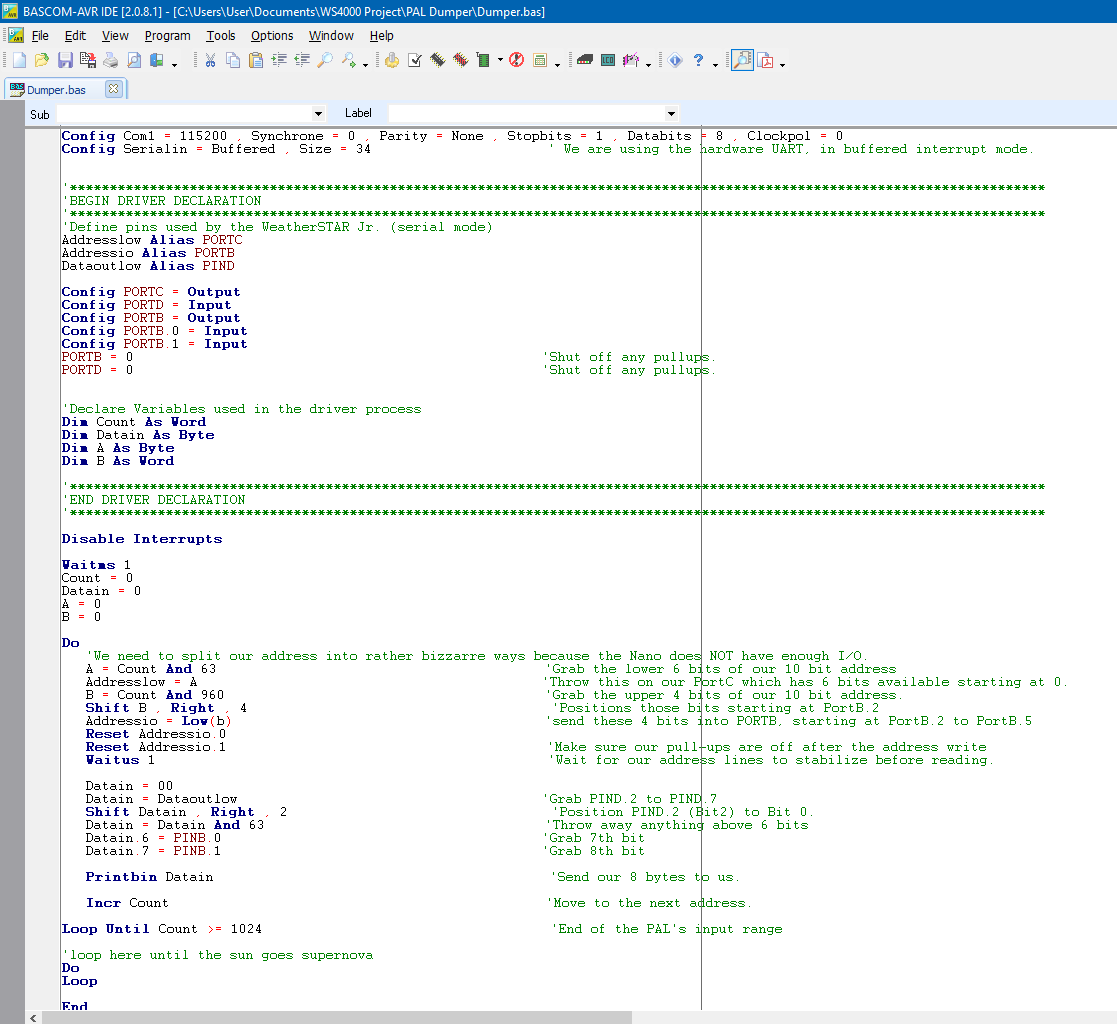
First thing is first though, We need to dump the PALs like a ROM. So, I used an Arduino Nano on a breadboard, I did not have a method to dump it with an external programmer. So I improvised.
Like So:
![]()
![]()
Ok, That part is done. But now, I have to write a program. Now, dont laugh! I really at this point did not know how to write code in C just yet. But I have written code in VB/BASIC all my life, and thats how I used these little microcontrollers.
Working with this machine actually taught me C. Surprisingly.
Anyways, Time to write a program!
![]()
Simple! well not really... i had to take some time to think, and then calculate how many iterations to read based on the number of inputs. i literally did this the hard way due to the reduced number of I/O on the Nano. I would read a block of bytes, then change the upper bits. i had 2 to 4 bits that the MCU didnt control. so i effectively made 16 dumps with 4 bits. Yeah, i could have used an arduino Mega and dumped the whole thing in one wack.
But, Lazy.....
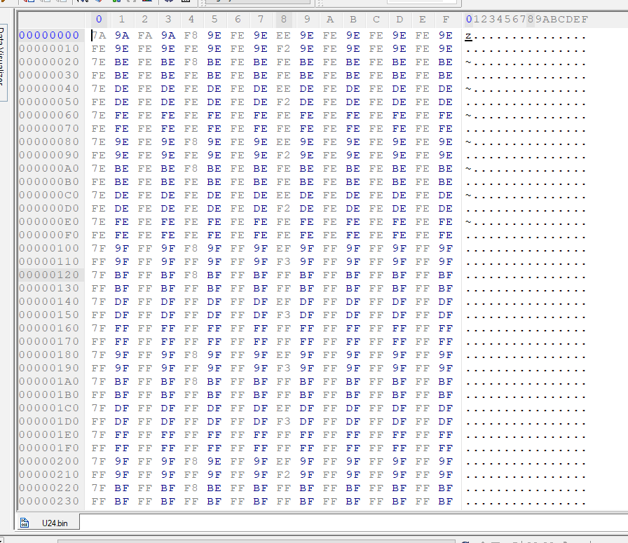
Then you end up with the dump, something like this:
![]()
That part is over. I dumped the rest of the chips and then stored the dumps for further processing.
The fun part is yet to come. Deciphering the PAL logic!
-
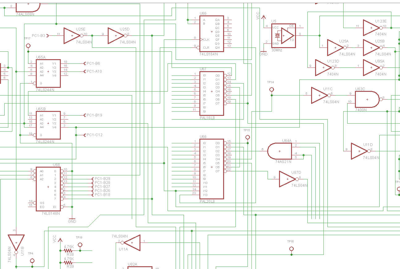
Logic Obfuscation
03/09/2021 at 23:50 • 0 commentsRemember the discussion I had earlier? Yeah, that's right. those pesky FPGAs and PALs.
So once we have the schematic drawn out, I can begin to stand back and take a big picture look at this thing and begin to study its design and architecture. However, you see things like this:
![]()
Basically, that doesn't really tell you a whole lot. Seems a lot of the logic is locked up inside those PALs. As seen above.
Another one:
![]()
The one I am most afraid of, is yes. the FPGAs and PALs associated therein:
![]()
We take a look at the CPU card, and more of the same:
![]()
Especially in the Bus/RAM sections:
![]()
![]()
I suppose using PALs and other logic arrays were not that uncommon in the late 80s, probably to keep cost down or board space usage down. But then again, looking at how this unit was engineered? I don't think cost was an object.
Regardless, There isn't any way around other than figuring out a method to reverse the logic out of the PALs. Luckily? the majority of the PALs are L style, or combinational logic.
There are a couple registered logic PALs on the graphics card, But... those still remain a mystery to this day. They appear to be gating for the pixel clock and a frequency divider for the PLL.
Next step..... figure out those PALs.
-
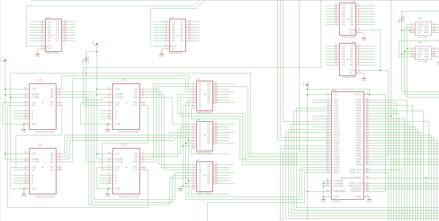
The Schematics
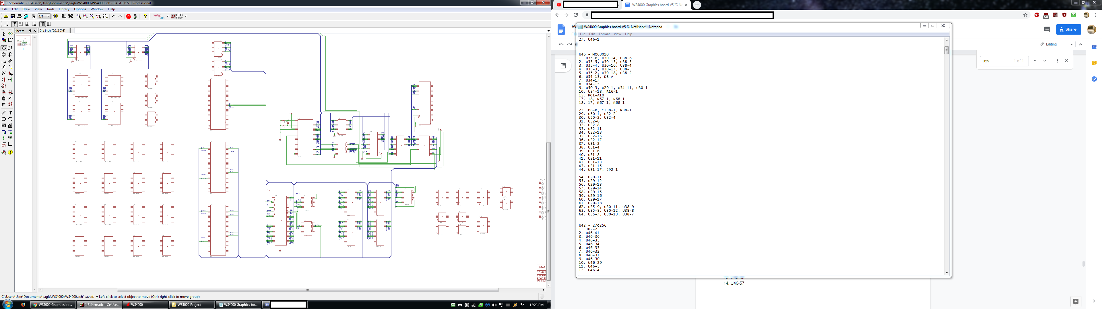
03/09/2021 at 23:31 • 0 commentsSo eventually I had to build my netlist on the graphics card, the CPU card, and all the other cards.
By the end of this, I was literally ready to go jump off a bridge. I had soaked up months and months of time into all of this. And this excludes work hours of course as I still have my day job.
I ended up doing the graphics card first, then working out reverse engineering it first. Once I had the graphics card done, I went back and did the rest a month or two later.
Eventually its all worth it in the end as the journey continues. It is a necessary evil if you wish to develop on a bespoke system that has ZERO documentation anywhere. (outside TWCs own archives).
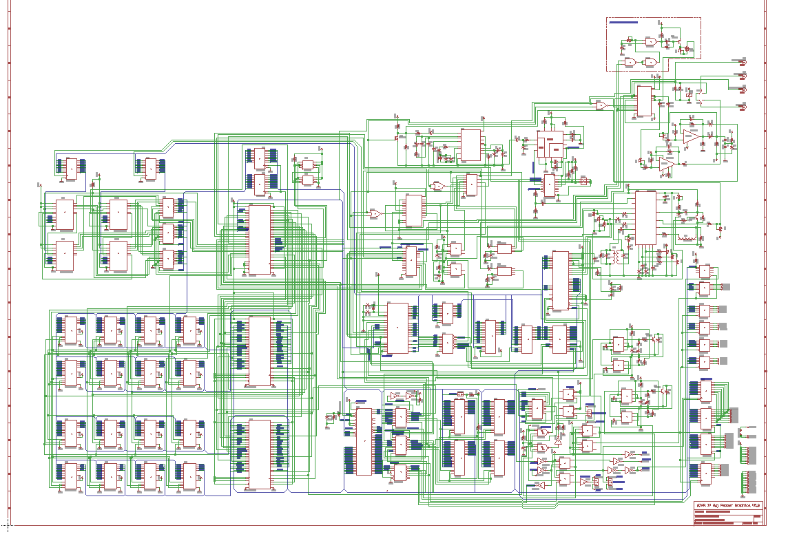
After all that work, you end up with the rewards:
Graphics
![]()
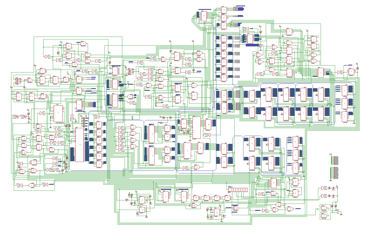
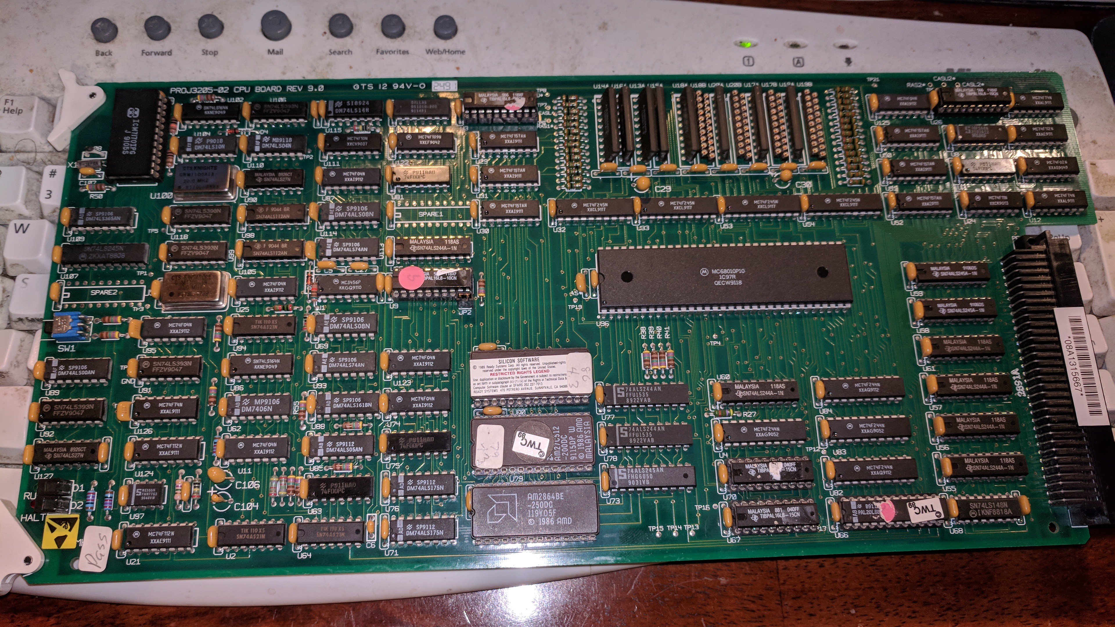
CPU:
![]()
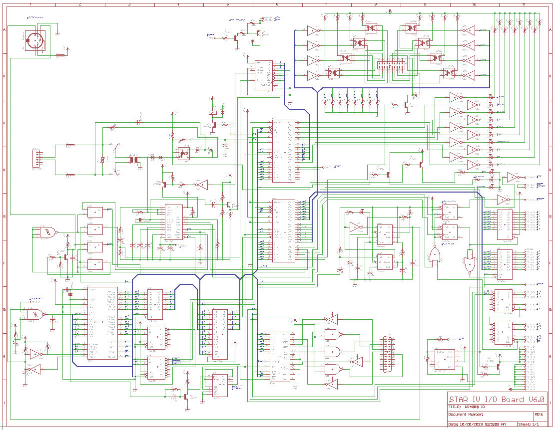
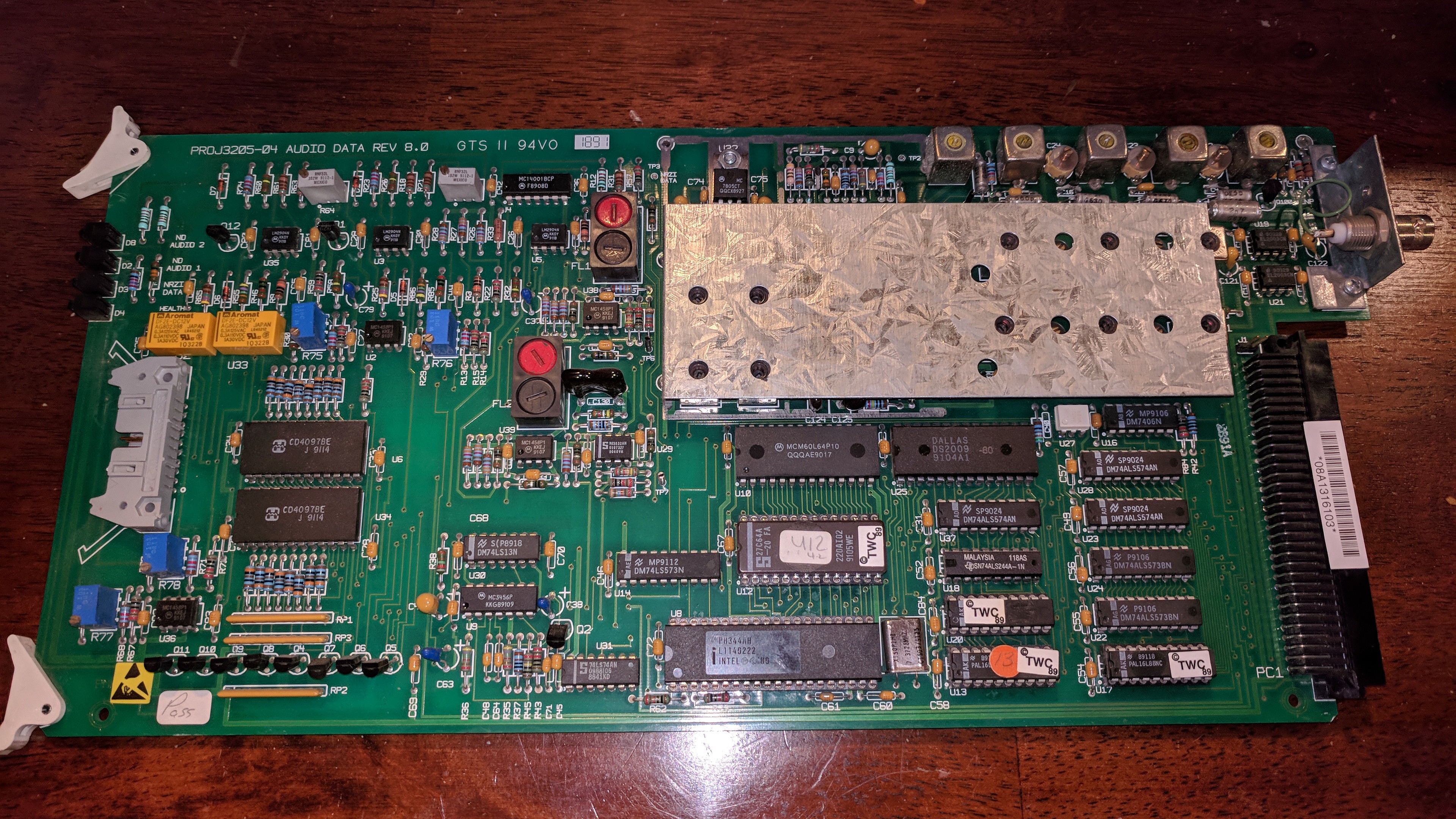
I/O:
![]()
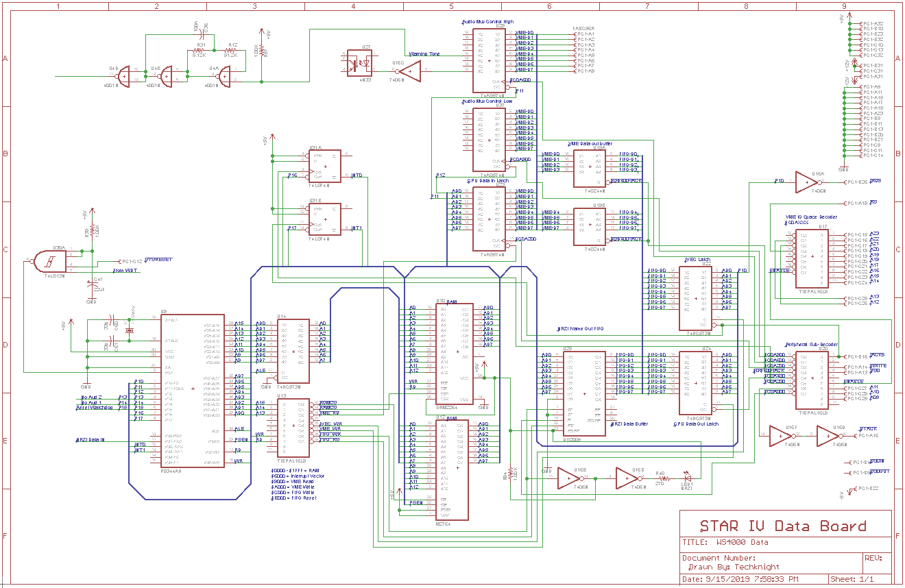
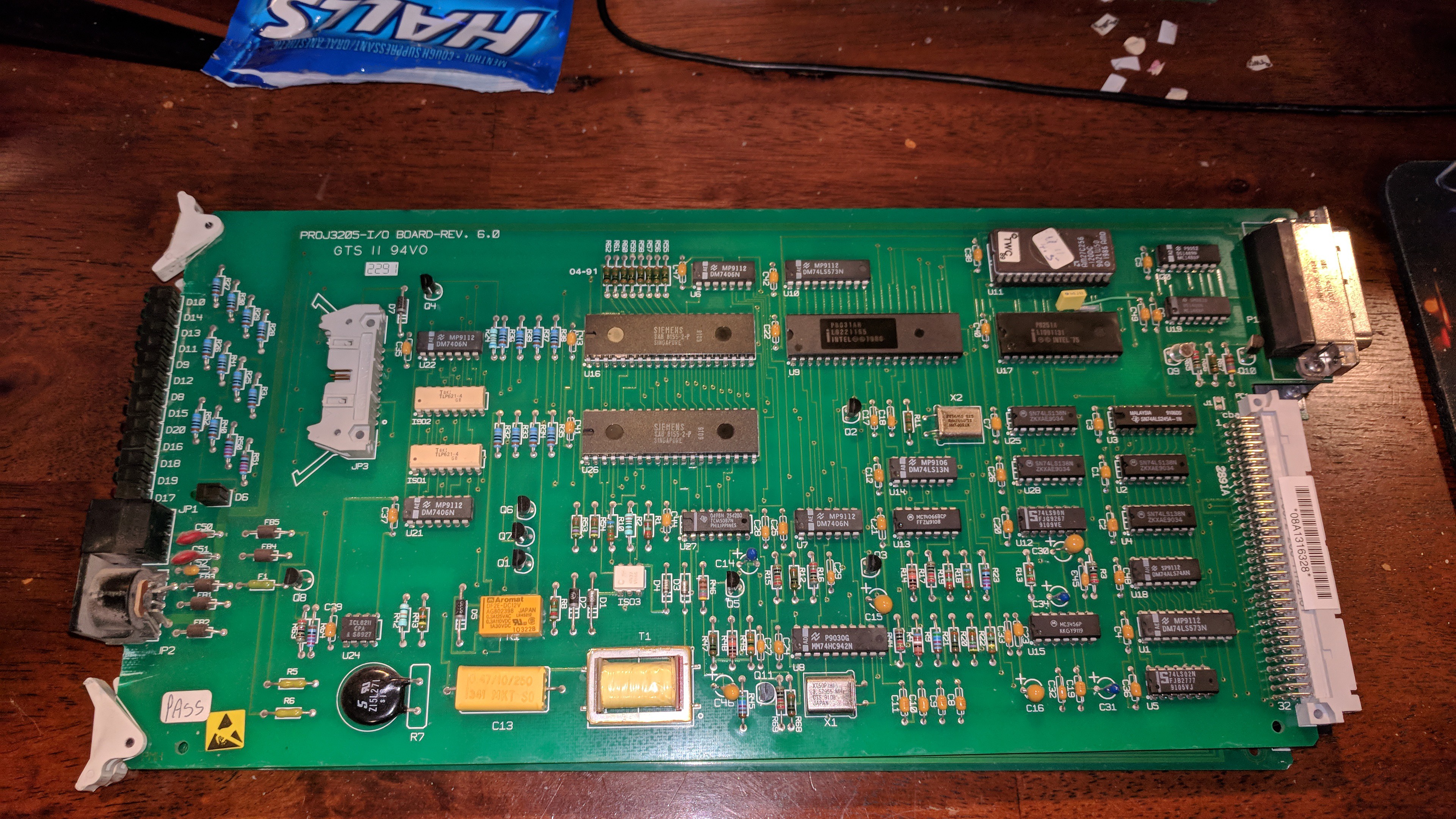
And by the time I got to the data card, I said screw it. I was done! I intended on replacing the data card with my own design, but we will get to that later. I documented just enough so I could figure out what to do with it.
![]()
Whew..... Well that's done! or... is it?
-
Buzzing out connections
03/09/2021 at 02:11 • 0 commentsFast forward to the first week of July in 2019. I was off work for a week, so it was time to get busy.
The only thing left to do at this point is basically start buzzing out the connections. This was a very painstaking process that took DAYS to perform.
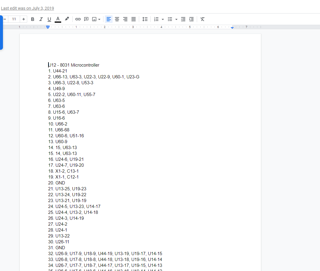
Basically, I started with every chip, Went into Google Docs (so i could do realtime saves) and put down the chip number/location, and pins. and buzzed out where they all went. I called this my netlist chart.
Did I mention that was a painstaking process? This was the only way I knew of on how to get the design into something I could work with and study.
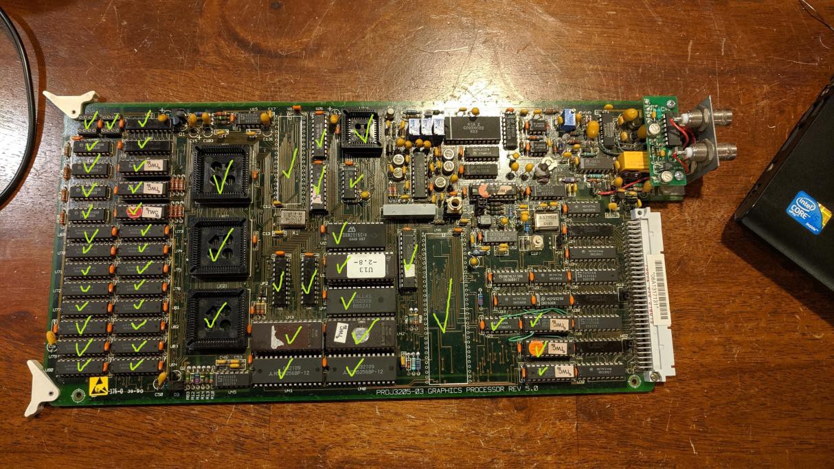
Basically started with this:
![]()
I had mspaint open on my laptop sitting next to the card, where I was recording the information as I went along. Basically checkmarking off one thing at a time as I did the work:
![]()
Then you have to catch mistakes as you go along. For example, as you branch out one chip at a time, eventually get to the chip at the other end. This will allow you to cross-check the connections you already made and check for mistakes. Oh.. and I found many. had to go back and double check multiple times.
Eventually after multiple days of painstaking eye-stabbing work, and needing a neck brace afterwords, you end up with this:
![]()
Granted, this is just one board! There are still 3 more to go after this one. WHEEEEEEEEEEE i just wanna go jump off a bridge at this point. Luckily, I didn't. This took some serious dedication.
Eventually, you end up with something like this:
![]()
This is great! but... not really helpful. Now it was time to spend another few weeks on turning that into a schematic.
By the end of this, I was extremely exhausted. Going it alone was starting to take its toll by this point:
![]()
More later....
-
The FPGAs
03/09/2021 at 01:01 • 0 commentsI knew I was going to have to cross paths with this eventually. the FPGAs. the Graphics board uses 3 XC2018s. the XC2064 was an iconic FPGA, one of the first ones released, and was heavily documented and reverse engineered.
the bitstreams are stored in the two XC PROMs in the upper left corner of the graphics card. the FPGAs themselves read out that bitstream, and when its fully read and configured, the FPGA asserts the DONE signal. This will release the board from RESET.
There are ways to reverse engineer the bitstreams back into logic. Sadly, I had no idea how to do this or had access to that, so I began posting around.
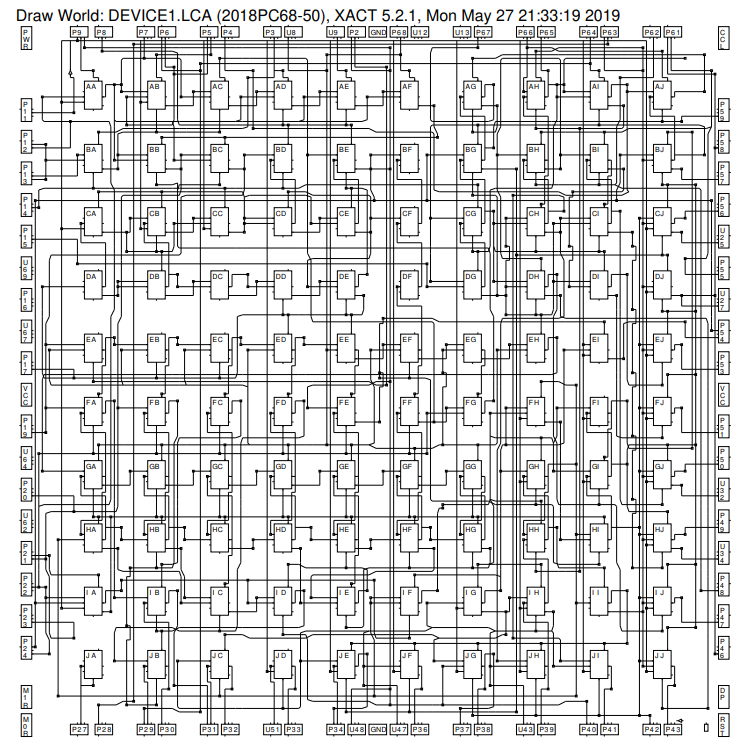
There was a guy on github which I ran into and he was gracious and invited me to a private github which contains scripts and code that he create to attempt to reverse the bitstream from an XC2018 back into XACT logic.
However, I did not have XACT and its hard to find out there on the internet. its an old DOS program and it works with these old school chips. Luckily he sent me his copy in private.
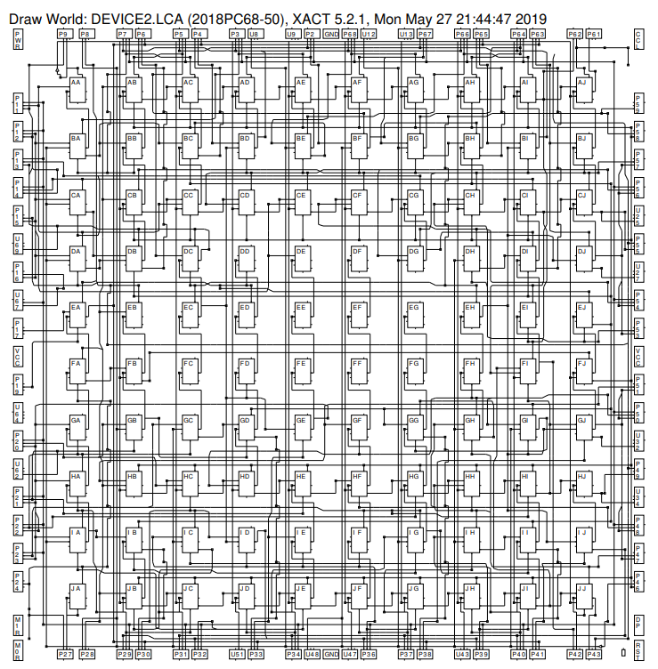
So after running the scripts to try and reverse the bitstreams, i got multiple errors and reported back. He attempted to fix the errors, and i was able to run the scripts successfully and get back xact logic!
Here is the logic that XACT was able to read from the chip closest to the 8031:
![]()
The bottom two chips appeared to have identical logic, and once I did some buzzing out of the circuits, they are probably the interleaving muxes.
![]()
I was thinking COOL!! This is really badass. I can actually see the logic that was in these chips. I was hoping this would help uncover some black magic. Especially since the 8031 chip's UART is configured as an SPI port, and its clocking 8 bits directly into that device1 FPGA.
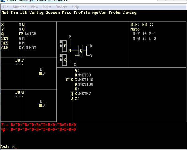
I started inspecting things in XACT, like so:
![]()
However, if you look closely at the XACT logic diagrams, there are lots of sections that appear "disconnected" and/or doesn't make sense.
Turns out, there are flaws in the reverse bitstream script. Sadly, those flaws were never fixed.
Ultimately, I had to abandon the idea of going directly after the FPGA logic to figure out how things are done. Could someone else potentially take this bitstream and then figure out where I failed? Yea probably. Matter of fact, I am hoping so!
But, I failed at this. So I had to move up a layer. Seeing that the 8031 is connected into the FPGA array and seems to be intermingled with that circuit, I quickly made an assumption that the 8031 is the framebuffer control CPU. So I went after it's ROM instead to figure how to talk to this chip.
If you cannot control the framebuffer? Then again as before, the whole thing is pointless. Since the FPGA black magic didn't work out, I had to do the next best thing and study the AMI/Nortel/TWC ROM.
Oh well.... another roadblock encountered. I was feeling pretty deflated, losing motivation and getting depressed and thinking I may not be able to crack this.... Well, at this point all I could do was move on!
-
Studying the ROMs
03/09/2021 at 00:16 • 0 commentsBetween the time period of January of 2019 until about June, i got involved in another project that was pretty much a stepping stone to this one. I dont know if its worthy of having another project blog on it or not since it was fairly simple compared to this. Anyways...
In the "lull" period of those few months, I decided to start diving further into the ROM to see if I could figure out anything that could aide in the process.
Again, I didn't know the 68K at all from a software/ASM standpoint so this was going to be a challenge. I found several sites teaching the 68k. one of them being Marky Jester's tutorial site which proved to be a very educational tool for me. I found another one based around the Sega, and that helped with some learning as well.
I tried contacting Steve at BMOW to help me, but he was very busy with life and other projects so he was unable to lend a hand. So, on to other avenues I suppose.
I contacted Marky directly to see if he could help me out with studying the ROMs. He tried to analyze things, gave me tips and hints, and also said there were some very math intensive routines in the graphics ROM. I am assuming that is a ROM-based vector graphics library which unfortunately, I have not figured out how to use those. I don't know the arguments and their types.
This was his best guess analysis:
![]()
![]()
Although his assessment was more or less guesswork since he, nor I, understood the hardware yet, it was a really good first attempt. Especially at helping me understand the ASM and how things work.
Ultimately, he figured out that the majority of it looks like it was written in some other high level language and compiled down due to how the stack was manipulated from subroutine to subroutine.
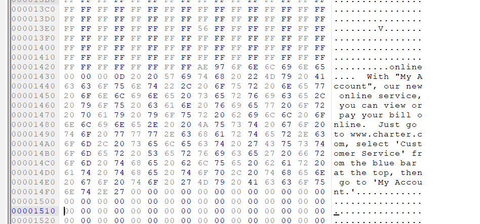
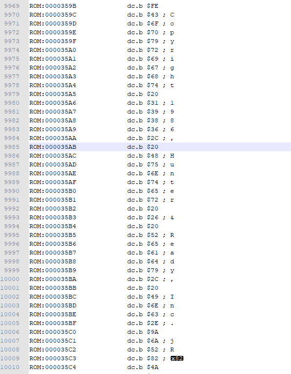
I did manage to take a peek at the other ROM/EEPROM dumps, and found neat things like this:
![]()
Neat! This is where the advertising crawls shown on the LOT8s were stored. in an AM2864 EEPROM on the CPU card.
-
Sgt Pepper Graphics
03/08/2021 at 23:45 • 0 commentsAt this point, I am committed, I wasn't going to let the 4000 go out in the night without any fanfare. I had to awaken the old beast and get this machine working again. I had a conversation with one of the original graphics designers of the 4000, Mike Searce.
He explained how things were done from his end, and that the graphics card was codenamed: "Sgt Pepper" Which i love things like this. its like archeology to me.
I wanted to start at the head of the snake first. The graphics card. because if I couldn't figure out the graphics card on a graphics machine, this whole project would be dead before it started. (btw, there are still mysteries to this day). This card was intimidating to look at, at first due to the multiple PALs, and the 3 FPGAs obfuscating tons of the logic, so I knew I was in for a major time with this.
First thing I needed to do is figure out what the bus standard was. I started chasing out the CPU card first to the eurodin slot to see if it matched up with anything out there. Turns out, the Data and Address lines as well as a few other lines matches up with VME Bus! I also had some help from a wonderful person who was a second set of eyes and confirmed it could be VMEBus.
However, as we will see later, Nortel/AMI did not use the VME standard as-is. they kept alot of it the same, but they changed how the interrupt lines are handled to free up pins for other voltages, plus a handful of other things. Moral of the story: Don't go plugging in standard VME devices into the backplane! bad things will happen. But its a major leap forward to figuring it out at least.
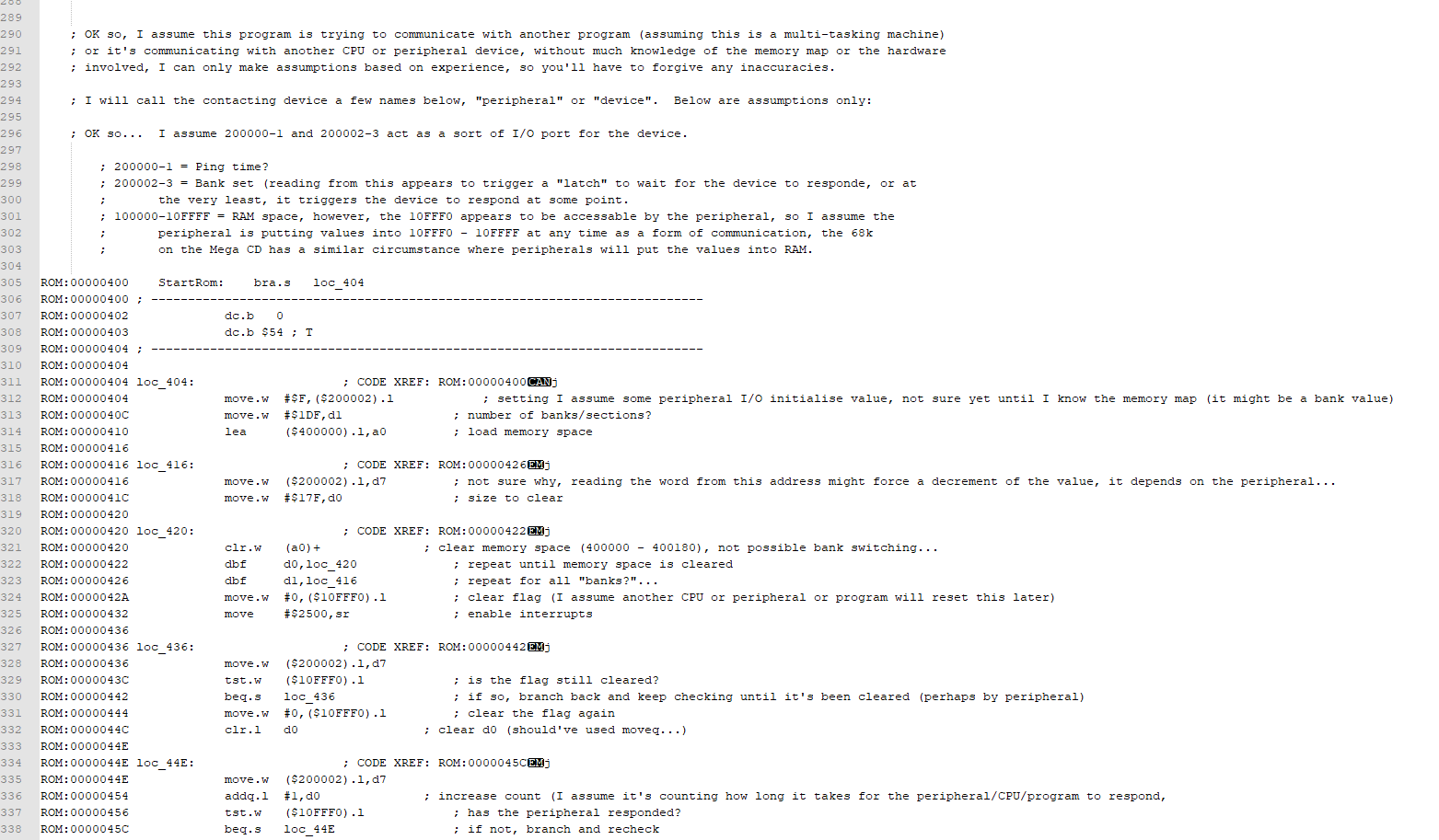
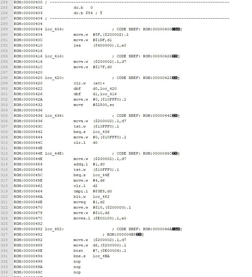
I then decided to start checking out the ROM. Well, the ROM wasn't making a whole lot of sense because I did not know the board's address map where everything is. On top of this, before this point, I only knew the 68K hardware and bus cycles. I knew NOTHING about the assembly language of the 68K at this point!
![]()
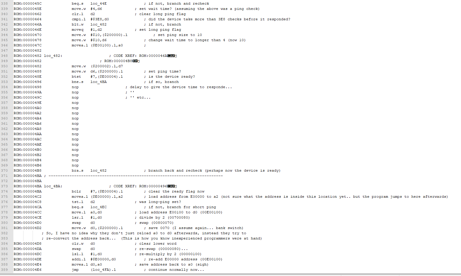
One thing that did stand out to me was this:
![]()
Hunter and Ready Systems Inc. Well that's a pretty good giveaway who did the ROM. So, I did some googling and found out that they did the Versatile Real Time Executive OS, or VRTX OS for this machine. But, alas, I had no manuals or even know what to do here yet. Nothing was making sense at this point. So i figured the next move is to literally go through the board, point to point, and buzz out the connections into a netlist. a Fluke multimeter and Google Docs to the rescue!
-
The Hardware
03/08/2021 at 23:23 • 0 commentsSince at this point I have pretty much figured out that I am on my own with this, with the exception of a few good friends for support, I decided to start my journey. Now that the preface is over, its time to move on!
So the first thing I decided to do was stare at the PCBs a little bit to at least determine the hardware. And this is what I have gathered:
CPU Card: contains 4MB of DRAM, and an MC68010 CPU.
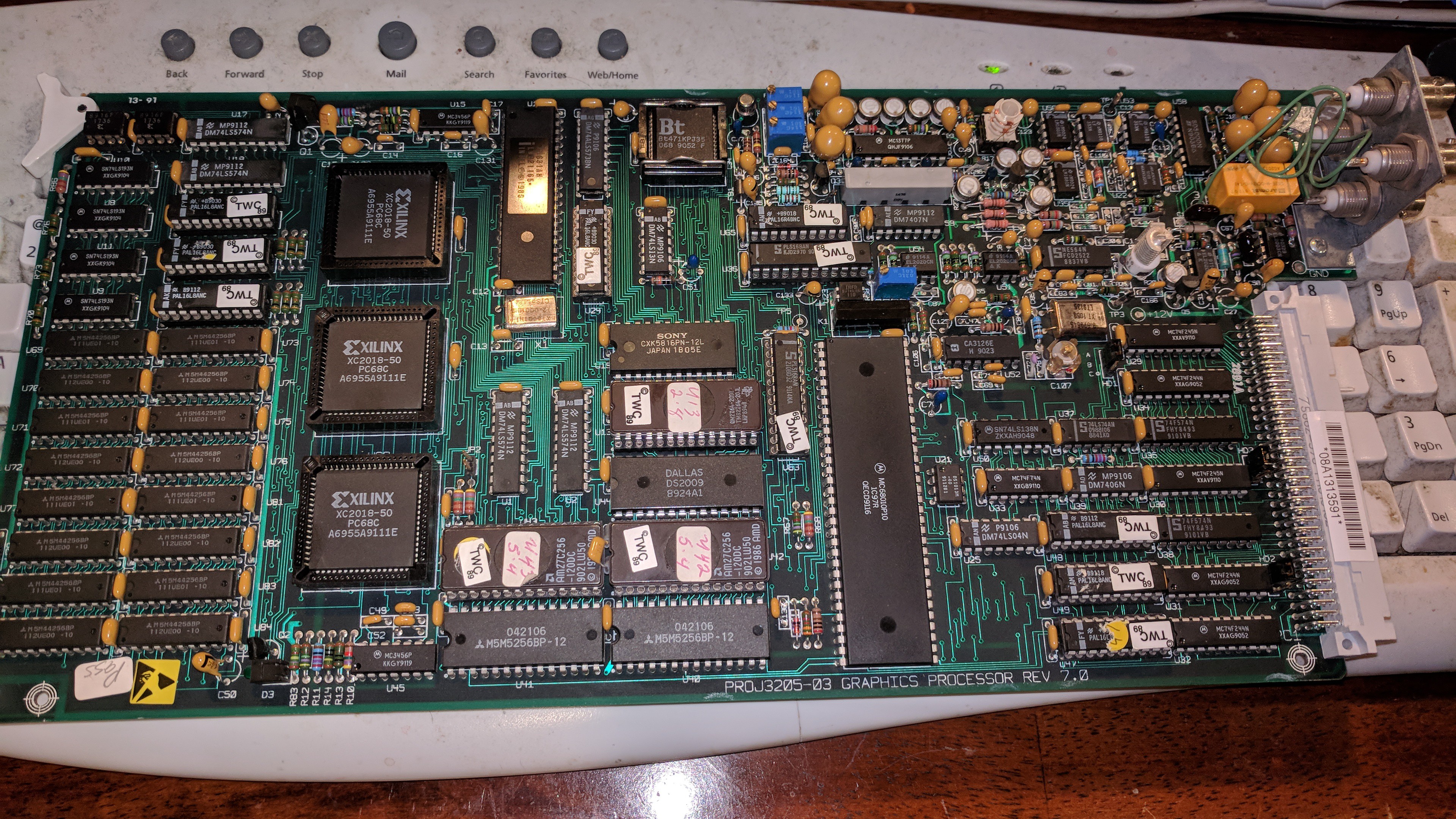
Graphics: This one is interesting. it contains an MC68010 CPU as well, AND an 8031 CPU (MCS51).
I/O card: Contains two PIO ICs and an 8031 CPU as well as a standard UART IC.
Data Card: This one is dual purpose, it has the audio and data circuitry on it as well as a 3-channel analog radio/RF stage for the various subcarriers. It contains an 8044 CPU which is a strange one. From what I could google, that chip is basically an 8051 with an SDLC controller instead of a serial UART. thats how I figured out what data it accepted, I was able to disassemble ROM to figure out how it initialized the SDLC transceiver.
Do I think this thing was overengineered? Probably. Maybe for futureproofing. But... there were alot of questionable design decisions, and what I think are blunders/bottlenecks. As we will see
![]()
![]()
![]()
![]()
Here is a video I published on youtube outlining the hardware:
-
Social Networking
03/08/2021 at 22:54 • 0 commentsThe next step in the process was getting a brief overview of the hardware that this thing is carrying, Dumping the ROMs to take a peek at the code, and then... potential networking with others in the TWC/Retro-computing hobby to see if anyone could have potentially saved the code when the feed was still online. So, I was reaching out to anyone I possibly could have.
Sadly however, to my knowledge, nobody was able to capture the data from the feed to be able to replay later. the data frames were SDLC frames at 115.2Kbps, over an FSK subcarrier. So without the proper hardware, its just not easy to do. Maybe with a sampling logic analyzer with the ability to record, or using a SDR radio to demodulate the signal and just store it into a bitstream. Something. But alas, no. I connected with an individual who had run these machines in his house when they were still operating, and he tried various methods within his means to record the signal, but all attempts failed since you need the correct setup to do so. And I don't have a time-machine so I cannot go back and capture the signal. :-(
So the moral of the story is: The software is lost, and never to be recovered again. TWC likely got rid of the VAX machines that ran these, and wouldn't talk to me anyways, the original designers have long since retired and don't have any of the information either, being 30+ years ago, their memory of specifics is fading.
There is also no documentation or schematics, or engineering diagrams for this machine. it literally was a mystery box of retro-computing hardware. So with that said, I was pretty much stuck to start from scratch.
Luckily, the circle of friends I gained had crisp crystal clear reference footage I could go by. And, on top of that, he still retained the original capture machine he used to record the system while in service, as well as the system itself. This proved to be vastly helpful for reproducing the correct colors, since he could verify color output on the same machine as the reference footage, and same recording device. So I could quickly compare his footage against my software output and compare the differences. This allowed me to recalibrate all the color values. They should be accurate. But, more on that later.
Anyways. Now it was time to start studying the hardware.
Reverse Engineering The Weather STAR 4000
The Weather STAR 4000: A Journey of reverse engineering the hardware to an iconic machine of the 1980s/90s.