-
Second assembly and testing
03/22/2021 at 04:20 • 0 comments03/21/2021
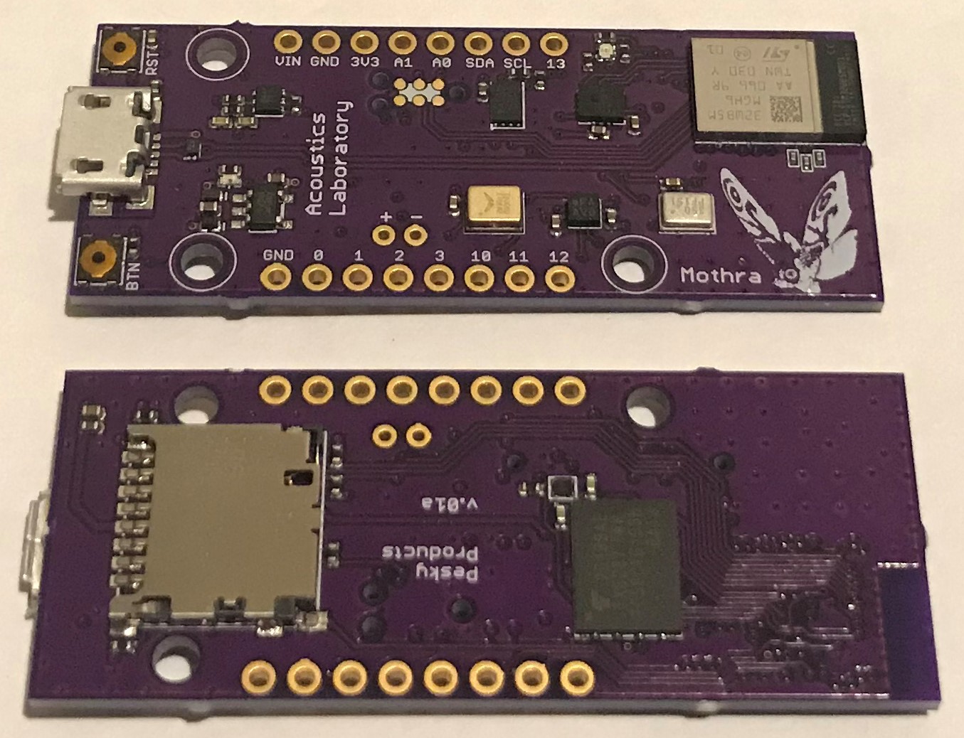
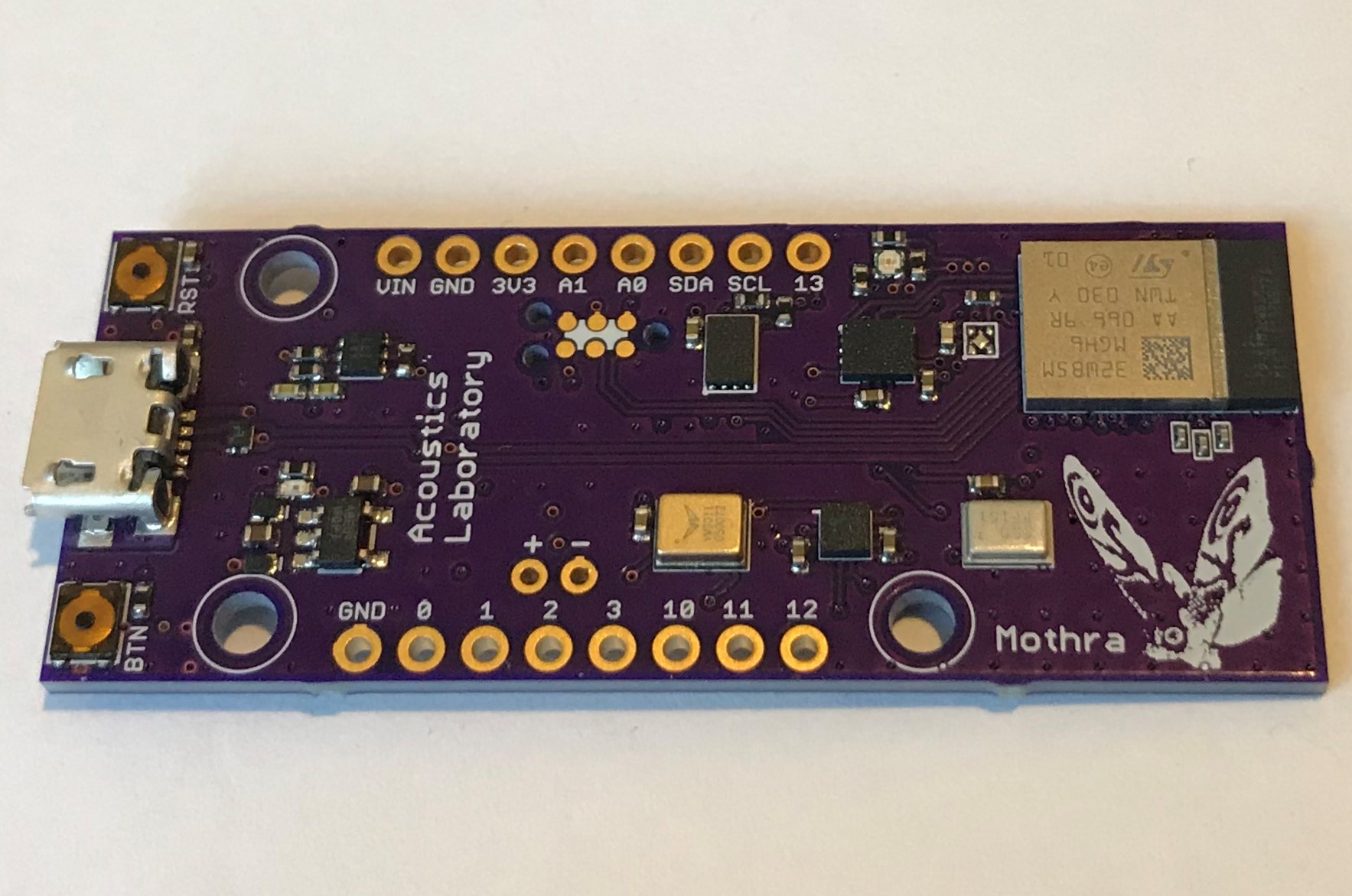
Got the revised pcbs back from OSH Park and put a couple together today.

Happy to say no shorts or design errors....yet.
Thomas Roell provided a preliminary Arduino core for testing the boards. I was able to blink the three RGB leds, read MCU temperature, and read battery voltage. I found all three I2C sensors on the internal I2C bus and was able to get the BMA400 to wake on motion and sleep on no motion. I verified I could record the sound of my voice using the ICS41350 PDM microphone. I verified BLE Tx using the Nordic UART service.
The RSSI of the module was around -50 dB when close to the smartphone. This is a little bit worse than what I have measured using the Firefly with the discrete STM32WB55 and its pcb antenna, which was somewhat surprising.
We have some more software development before we can test the IIS3DWB. And for some reason I wasn't able to get the SD card to work yet. Still, for one day's worth of assembly and testing the design seems to be working about as well as can be expected.
I ran a simple blink sketch with the MCU put into STOP mode for five seconds at the end of the main loop and used an ST power meter to check power consumption. The Mothra device is using ~210 uA in STOP mode, where it really should be using ~20 uA. So somewhat of a mystery here as to what is causing the extra 10x power usage in low power mode.
Early days, still a bit of work to do before we can start using the device as intended...
-
First Assembly
03/12/2021 at 22:36 • 0 comments03/08/2021
It's always fun to get the first boards from OSH park and spend some time assembling them. This is when you find out what dumb mistakes were made in haste. And of course, after putting two of the Mothra.v01 pcbs together, I discovered that I had swapped VDD and GND when connecting the power-control LDO to the NAND flash.


I had to remove the LDO to avoid the resultant short. This means that every component on the first version except the NAND flash should work as designed or at least be testable.
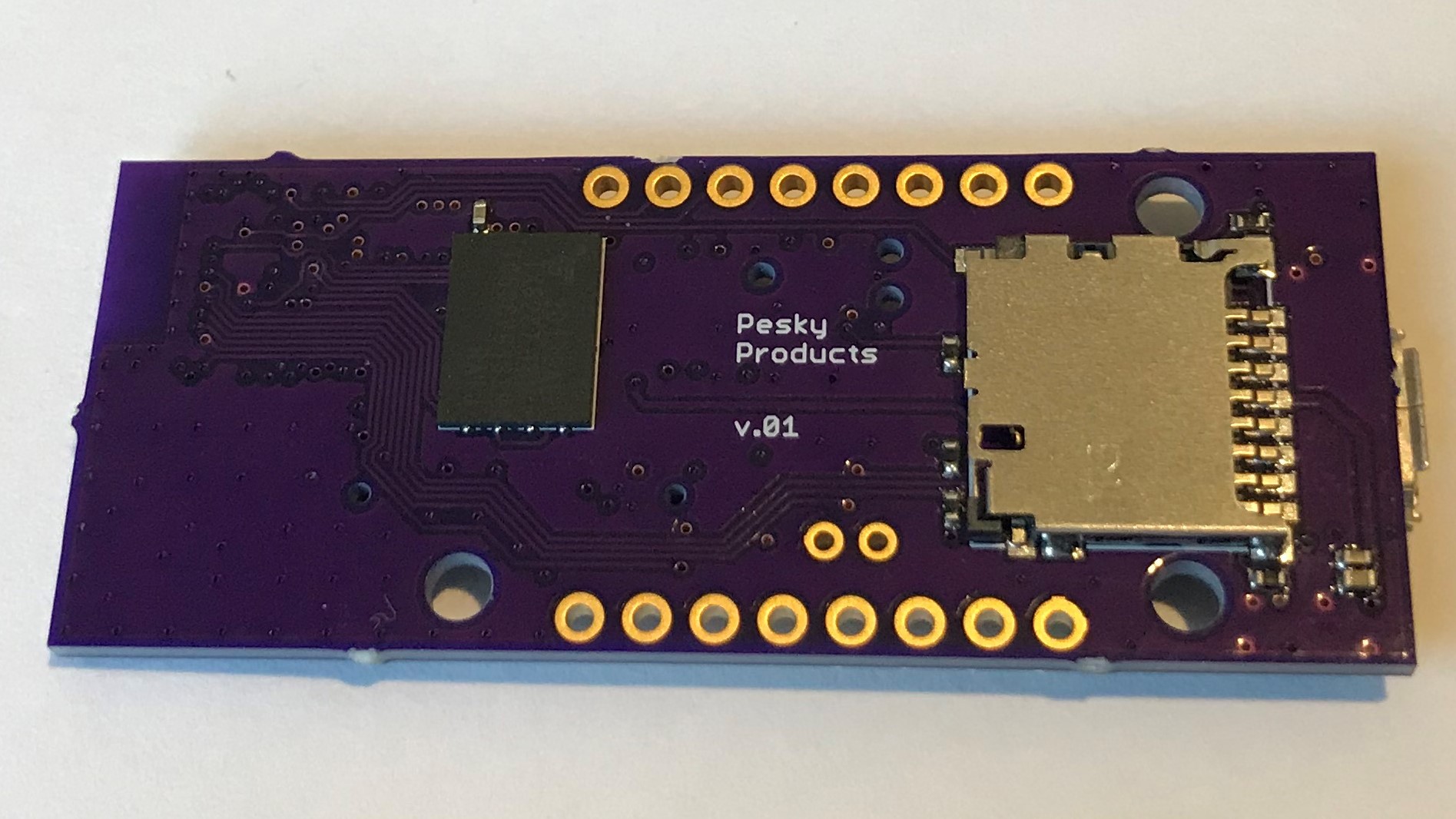
You can see the trace fanout on the bottom layer for the QSPI IIS3DWB and SPI SD Card et al. The design rules "require" that all traces route out of the bottom of the module such that the area to the right (in the above image of the board bottom, the area bottom left) of the module remain free of components and signals and be covered with ground plane and vias. This makes the trace traffic mighty congested even on a four-layer pcb; the second and third layers look about the same as the bottom one.
The STM32WB5MMG module embeds a STM32WB55VG 100-pin WLCSP and there are 85 total pins in the small 7.3 mm x 11 mm module.

I was worried that the 0.435 pitch pins on the periphery might be hard to solder. However, I found it was surprisingly easy using my usual 26 gauge syringe with low-temperature solder paste and a combo quartz heater plate and hot air gun.
This was my first experience using 0201 passive components. Three sensitive pins require 3.3 nF filter capacitors near the module, which are recommended to be 0201 (or smaller!) Somewhat to my surprise, these were as easy to use as the 0402 passives I regularly use. I am tempted to start using this package size more often, especially in very small designs.
I remember when I ordered some 0201 caps by mistake years ago (I still have them) and thought "there is no way I could ever make use of these!". What seemed impossible then will become a matter of course soon enough...
The fix to the botched circuit was easy to affect and we should have Mothra.v01a pcbs available soon. In the meantime, we are testing what we can using the wounded boards.
Mothra: Acoustics Laboratory on a Stick
STM32WB55 host with microphones and accelerometers and lots of memory for vibration and sound analysis
 Kris Winer


