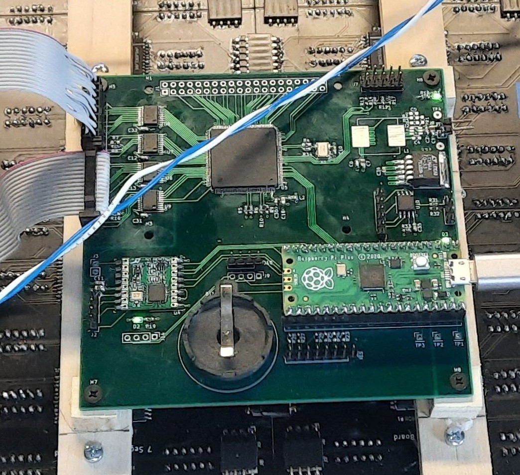
Unfortunately as I was excited to the display going I did not do much to document the control board assembly. It went fairly well. No white wires were needed as of yet. Only oppsie so far is that the two connectors for the display chains are about .05" to close to allow two ICD connectors to plug in. Had to create crimp connectors for the other.

Things tested:
- Power Supply (ditched the switcher and just used the linear regulator)
- Pico is up and running
- FPGA comes up and configures
- All SPI outputs for the display matrix are working.
Things to tested: Basically everything not required to make lights blink...
- Real time clock.
- Temp sensor
- RF Module
- ATINTY for IR receiving
Basic FPGA operation:
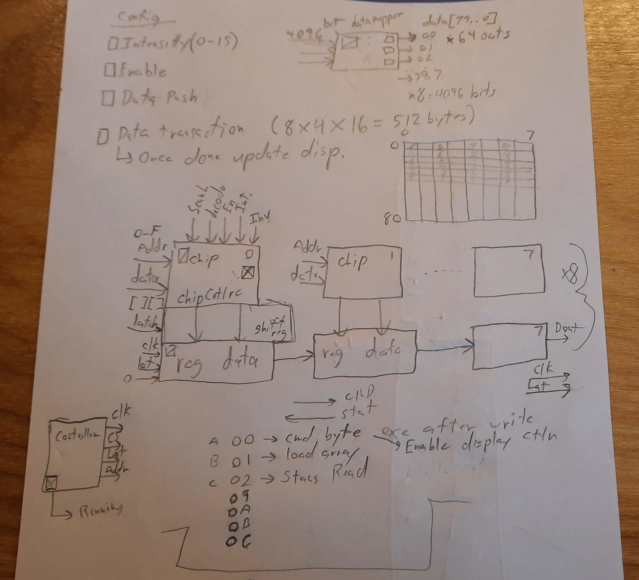
The FPGA is fairly straightforward. Below is a list of the major modules and my "block diagram" of the internals. I can provide more information if anyone is interested in how it works.
FPGA Modules:
- SPI Controller - Allows the PICO to control the matrix over SPI
- Data Mapper - Maps the data from the XY display RAM to the segment memory
- Chip Controller - Handles the configuration and programming of a single MAX7219
- Display Controller - Handles the clocking and addressing of data form the Chip Controllers
- Matrix Core - Implements the 8x8 grid of chip controllers, attached to the display controller, Data mapper and display RAM. This is where most of the work gets done.
FPGA Block diagram:

 seasleyece
Discussions
Become a Hackaday.io Member
Create an account to leave a comment. Already have an account? Log In.