-
Fab Update and Firmware
08/01/2017 at 01:43 • 1 commentSo I'm really leaning towards macrofab for manufacturing, I've got the board uploaded and nearly finished configuring the components when I found a small issue. The issue is the coilcraft RF inductors are not stocked by by Macrofab for the quantity of boards I want to order and there is no indication of how many boards need to be ordered for them to stock the parts. I'm going to communicate with their customer service on how I should proceed, most likely going to buy the parts and supply them myself, or populate them myself post macrofab.
Moving on to firmware. At my place of work I've taken on a more systems engineering role so I am working with firmware engineers again and it has got my mind working again in regards to firmware.
For the S1G-RF firmware I'm planing on a state-machine bare-metal firmware design. In short it will boot up into a default state and await commands over a variety of interfaces and respond etc. From the perspective of the firmware each mode will be a state within the overall state machine despite them being referred to as modes. The mode terminology is uses to differentiate states that provide function vs ones that are for say pairing, house keeping, or processing. Tentatively I am envisioning the firmware to have the following states:
- Idle - The default state, boot up state, awaits commands to change modes into another state, or to resume previous state from its last power up.
- Configuration - In this state the the radio can can pair with another and form a link. After a link is established the radio awaits a command to select its mode of operation.
- UART Mode - This mode has the a radio talk over UART sort of like a virtual com port but wireless.
- SPI Mode - In this mode the radio will use SPI to communicate in a similar fashion as UART mode, think SPI virtual com port but wireless.
- USB Mode - This mode the radio uses USB to communicate, same idea virtual com port but wireless over USB.
- Serializer Mode - In this mode the radio will sample a bank of inputs and transmit them wireless, the idea will be for sending servo signals wirelessly etc.
- Programmable Mode - Programmable mode will be a mode that allows user code to run for custom applications, with all the radio control and pairing stuff handled in libraries. Make your own Sub 1GHZ RF devices essentially.
The listed states are not the only ones there will be, in the future as I come up with more ideas there will be future modes added for alternative operations/applications. The firmware is being developed in C using a makefile project exported by STM32CubeMX Studio (I spoke of this before but this is for the folks that have been following since the prize began etc) in a linux environment using the ARM GNU Toolchain. So far the driver software for all the required hardware peripherals on the STM32 has been configured and setup, it compiles just fine. Early on in the firmware development I found a non-RTOS C driver for the ADF7023, during that same time I go the driver to compile for the STM32 using the STM32 generated SPI library successfully. Shortly after firmware development stopped.Moving forward with firmware development the plan is to make a block diagram of the state machine and then turn the diagram into C code. This will make it a lot easier to write clean code and give me time to work out the states. All code will be published to the same github repo as before for those that want to take a look. Thats all for this update, another is on its way after I make my diagrams, stay tuned!!!
-
Fabrication Plans
04/10/2017 at 14:37 • 0 commentsIts good to come back to this project. The last few months have been very busy for me working a new job with a decent commute (not much time for hacks). Now that I'm used to me new routine at my new job I can manage some time to work on S1G-RF again.
Last time I left off I was starting the firmware. Getting back to it I'm planning to fabricate the board and build some prototypes then continue the firmware development process. At the last minute however I decided to have my friend and colleague Alex Camilo run through my schematic and board. He found a few bugs in my design that I didn't find myself nor did the other folks in my circles I shared the design with. I have since fixed the bugs (reference schematic not transposed correctly etc) my next phase is to think about fabrication.
Most of the time I use OSHPark for my prototype PCBs and populate them by hand but this time I'm not sure if I'm going to go that route. The reason being is that components are pretty costly for the ADF7023's supporting passive components, particularly the RF inductors. Another reason is the design while simple on the surface is a rather complex one to assemble and to assemble correctly, I'm afraid I might make mistakes that will make debugging the protos a headache. So I have been considering using macrofab for manufacturing a small prototype batch. They will assemble them without issue and any bugs in the design should be my fault etc is the idea.
I appreciate the continued enthusiasm for this project and my many others and I hope to make more time to dedicate to this wonderful community that has brought me so much!
Stay Tuned folks !!!
-
Project Update: Firmware and Hardware Changes
12/19/2016 at 23:08 • 0 commentsHey folks! this project has been on the backburner for a few weeks while I've been tending to other matters. A few developments have occurred since the last update. Shortly after posting about the adapter boards in the last project log I started on the firmware.
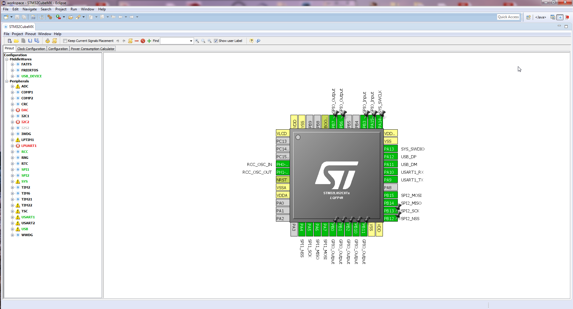
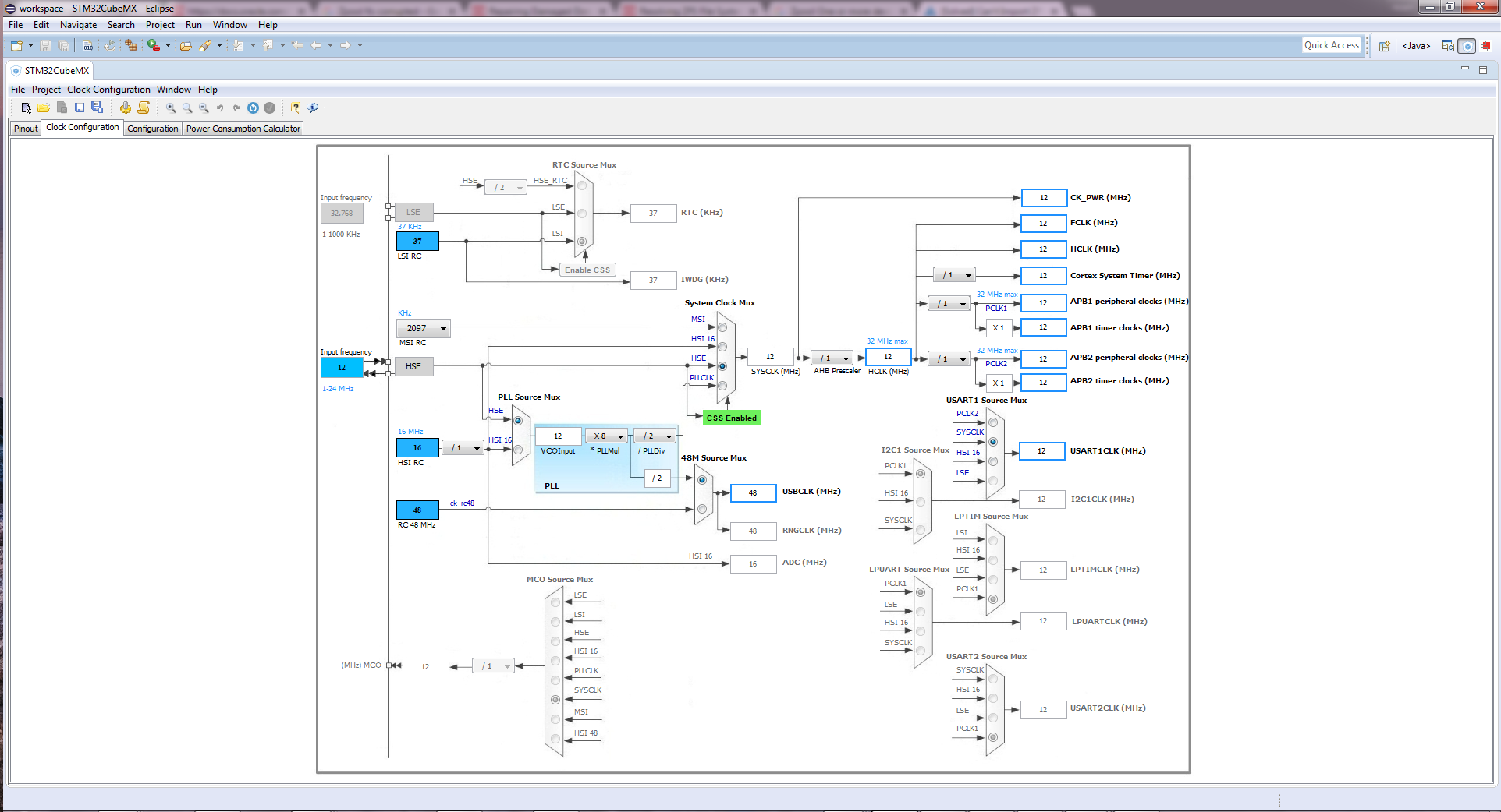
The firmware for the S1G-RF is going to be written in C using the manufacture libraries generated by ST Microelectronics' app STM32CubeMX. With that application I was able to generate all the driver code for all the peripherals in use on the STM32 for the S1G-RF hardware, this also includes USB virtual serial port code! STM32CubeMX is a simple GUI application and you just pick and choose everything you need, select the peripherals then configure the clocks, export code done, totally magic!
Peripherals selected and configured:
![]()
Clock Configuration:
![]()
After configuring all the peripherals and clocks on the STM32 the code is exported in the form of an Eclipse project, the flavor of which depends on which ARM IDE you select in the preferences, each option is effectively a custom build of Eclipse with an ARM toolchain and some GUI features shoved in it. Since I prefer to develop software on Linux and with a text editor I needed to convert the project to a standard C makefile format. To achive this I used a simple python script I found online, here it is:
https://github.com/baoshi/CubeMX2Makefile
Really easy to use and works like a charm. I am currently compiling and building the firmware with the ARM GNU Toolchain on Debian stretch using the makefile and code generated by STM32CubeMX and the python script. ARM GNU Toolchain can be found here for those of you that want to look at the code and compile it yourselves: https://launchpad.net/gcc-arm-embedded .
Now as far as the SPI driver code goes for the ADF7023 transceiver chip my original plan was to sleuth through the datasheet and write my own driver library, but fortunately Analog Devices did all the hard work. Turns out Analog Devices has a github page that has a ton of open source C drivers for many devices they sell. The repository is here: https://github.com/analogdevicesinc/no-OS it covers a lot of devices they have and assumes there is no OS in your application so these drivers are best suited for a baremetal firmware approach. The source code for the ADF7023 specifically is found here : https://github.com/analogdevicesinc/no-OS/tree/master/drivers/ADF7023 , it makes reference to another file pair called communication.h/.c where you need to implement a few functions for controlling the SPI peripheral on your master device, I simply implemented the functions as wrappers that call the STM32 SPI driver code. I only spent a couple hours working on the firmware but after a bit of reading compiler errors and debugging I got the ADF7023 driver code compiling onto of the STM32 peripheral driver codebase successfully. The project's firmware code can be found here: https://github.com/adamjvr/S1G-RF-firmwware all code that does not belong to ST Microelectronics or Analog Devices Inc. is released under the MIT open source license. Still much more to come on this, I'm still hammering out the overall functionality and when I have a clear roadmap I'll get back to writing more code.
At the start of the project log I mentioned some updates to the hardware. One of the updates will be adjustments made to the ground pours around the RF transceiver, RF amplifier matching circuits, and antenna connectors. I want to pull back the groun pours tad around the antenna traces and tranceiver, as recommended by the FaradayRF project. They are already several design iterations in on their 900MHZ radio and I appreciate their input! Please also check out their project too https://faradayrf.com/ if you are a ham interested in 900MHZ their platform is for you. Anyways back to S1G-RF!!! :) In addition to copper pour adjustments I want to had some small switch banks for setting which functional mode the S1G-RF is in. The switch will pull certain GPIO pins either low or high, when the STM32 onboard starts up it will read their pins for a 4 digit binary value. The binary value as set by the switches on the pins will correspond to one of the S1G-RF's functional modes. These additions won't take long to implement, after I get them in my plan is to go back to working the firmware some more before ordering PCBs. The idea is by writing the firmware now I will hopefully catch any possible mistakes I made in the hardware or perhaps learn that I need additional features for my desired functionalities. Anyways more to come on this project, soon I'm just getting started :) !
-
Small Update
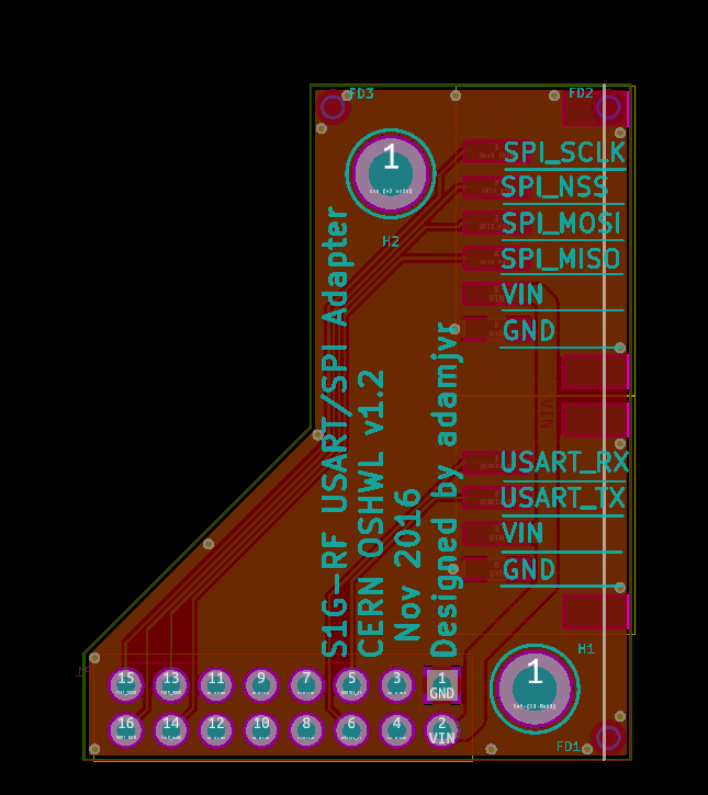
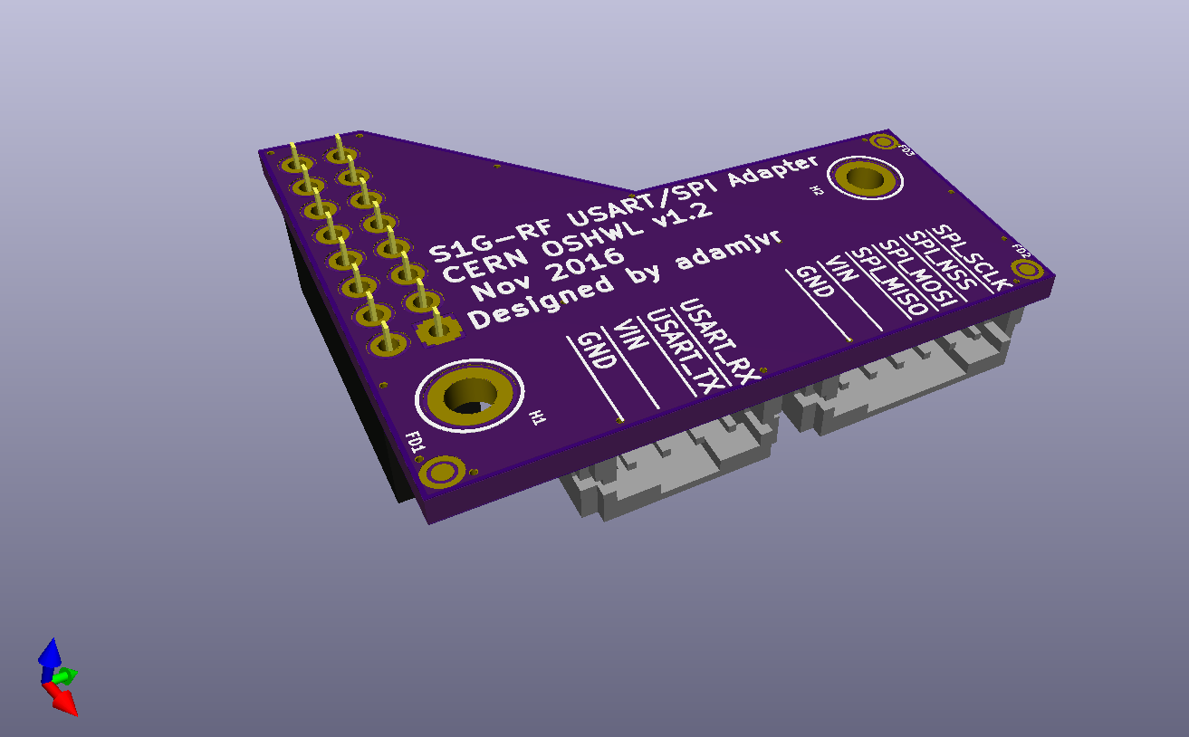
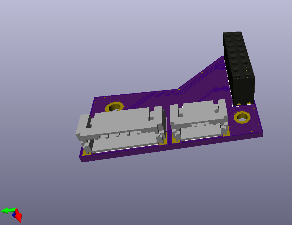
11/14/2016 at 05:54 • 0 commentsSo, I've been researching and doing more tweaks to the radio PCBs. There's been a few commits to the git, mostly adjustments with grounding and ground pours. The main part about this update is the addition of an adapter PCB. This PCB converts the 2.54mm header into snap fit JST connectors breaking out the SPI to a 6 pin connector with power and ground, and USART broken out to a 4 pin connector with power and ground as well. With this addon adapter the S1G radio modules can be used by embedded devices in lieu of USB connectivity.
![]()
3D Views
![]()
![]()
The PCB press fits ontop of the radio modules and can be screwed down. I am going to design some 3D printable spacers/standoffs to sit between both PCBs. There will be other adapters down the line to make interfacing with the S1G simple for many different applications, there will also be a printable housing that supports these modular adapters. Stay tuned for more updates on the project!
-
First Pass of PCBs done
11/12/2016 at 00:20 • 0 commentsHey so I got a little ambitious over the last few days and did a lot of work to the PCB. I'm happy to share my first pass on routing on both PCBs for this project log. First off there were a number of changes to the schematic and the connectors used on the board, these specs are still subject to change over the course of the project. Anyways I swapped out the fancy SMT connectors for 2.54mm pitch pin header and broke out all the signals to a single header. This header allows the radio to communicate over SPI or USART, the header also allows for power to be fed into the board for applications where USB power is unavailable. I also swtiched to this kind of connector because its more popular and easier to interface with, 2.54mm Pitch is pretty standard.
So this project encompasses two versions of the same radio circuitry, one version with separate PA/LNA matching circuitry and antennas, the other one uses a combined match and a single antenna. The combined implementation is meant for application where size is an issue, the separate implementation is for size independent applications such as drone ground stations.
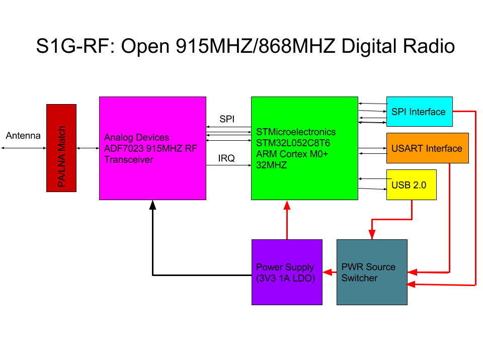
Before I unveil the PCBs, I wanna outline the general function of them, I didn't elaborate on that all that much in the first post. There is a diagram below to help understand:
![]()
The diagram above shows the general system overview of both of the S1GRF PCBs. The heart of both is the ADF7023 transceiver IC, this is controlled by an ARM Cortex M0+ over SPI serial. The ARM Cortex M0+ being used is the STM32L052C8T6 its a simple ARM micro-controller clocked at 32MHZ. The STM32's job is to provide a USB 2.0 interface, USART, and SPI interface for connecting to user applications. How these interfaces will function will be later defined when the firmware gets developed. Also the serial interfaces that are available on the pin connector along with GPIO pins. Also in the diagram is a power source switcher, this is essentially a simple circuit consisting of a MOSFET and diode, this switches the LDO to be fed off the USB port instead of the pin connector.
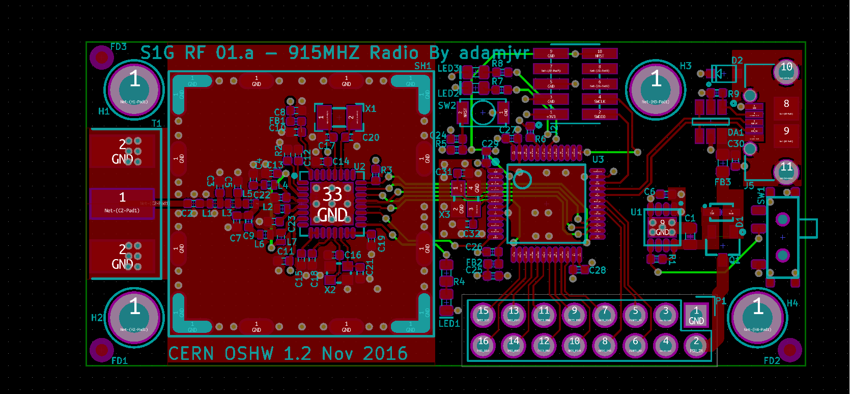
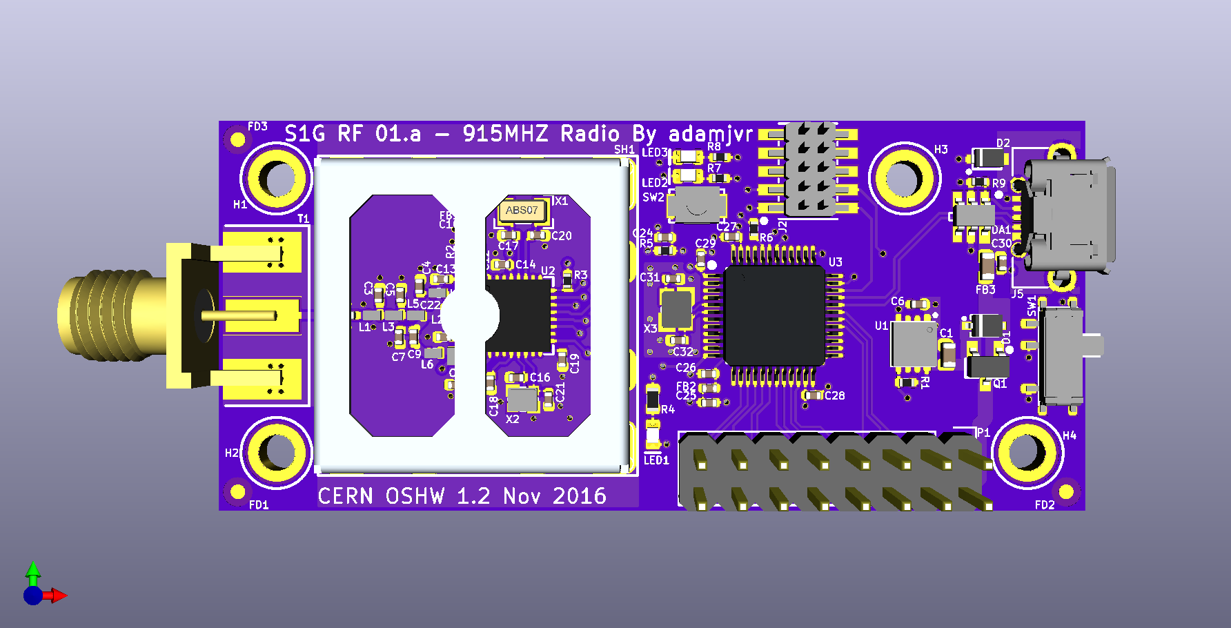
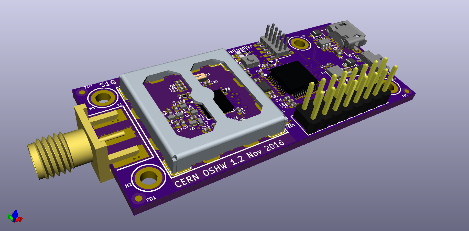
Now for the PCBs! First here is the combined PA/LNA match implementation:
2D From KiCAD:
![]()
KiCAD 3D Top Side:
![]()
KiCAD 3D Angled:
![]()
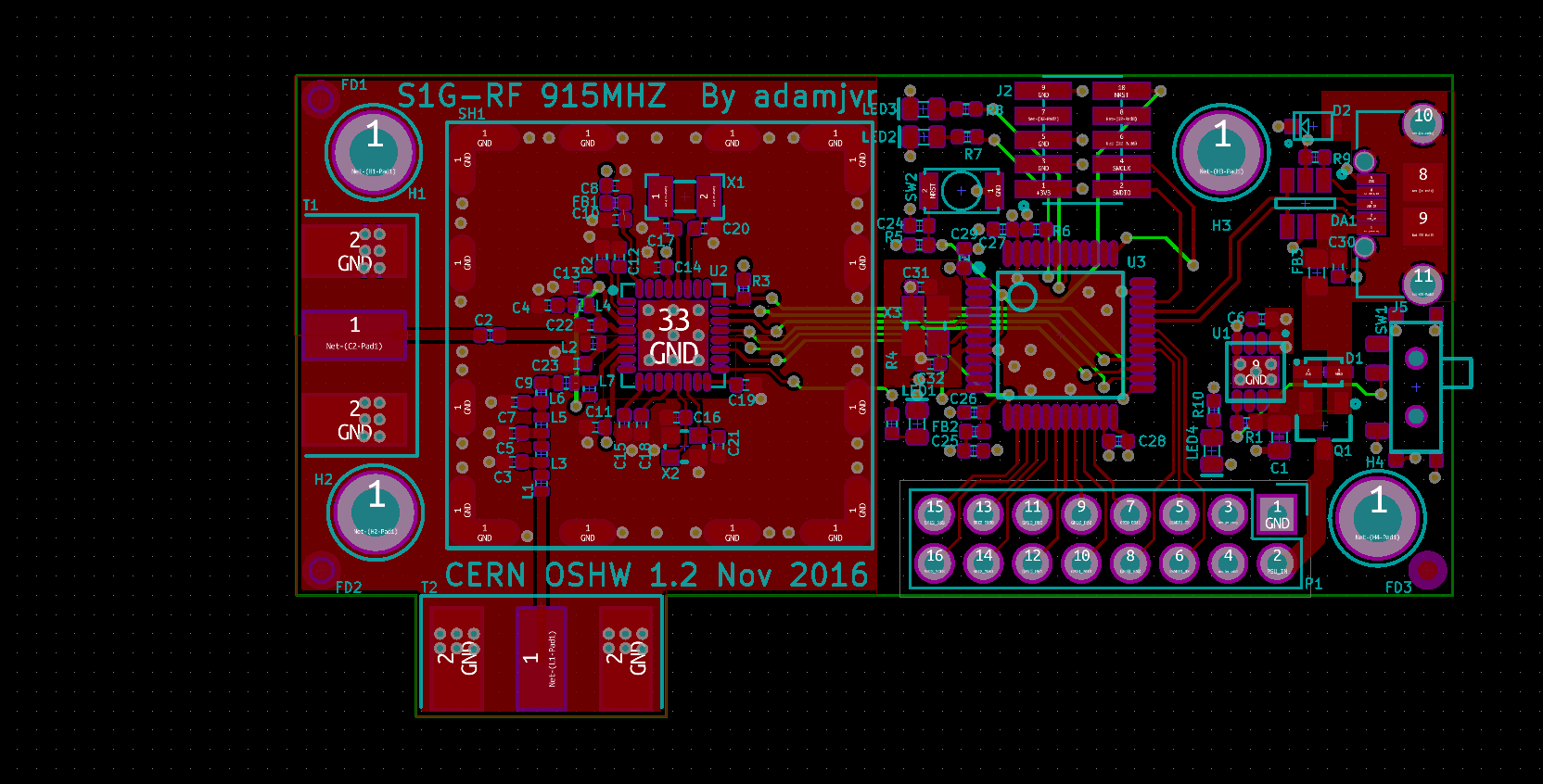
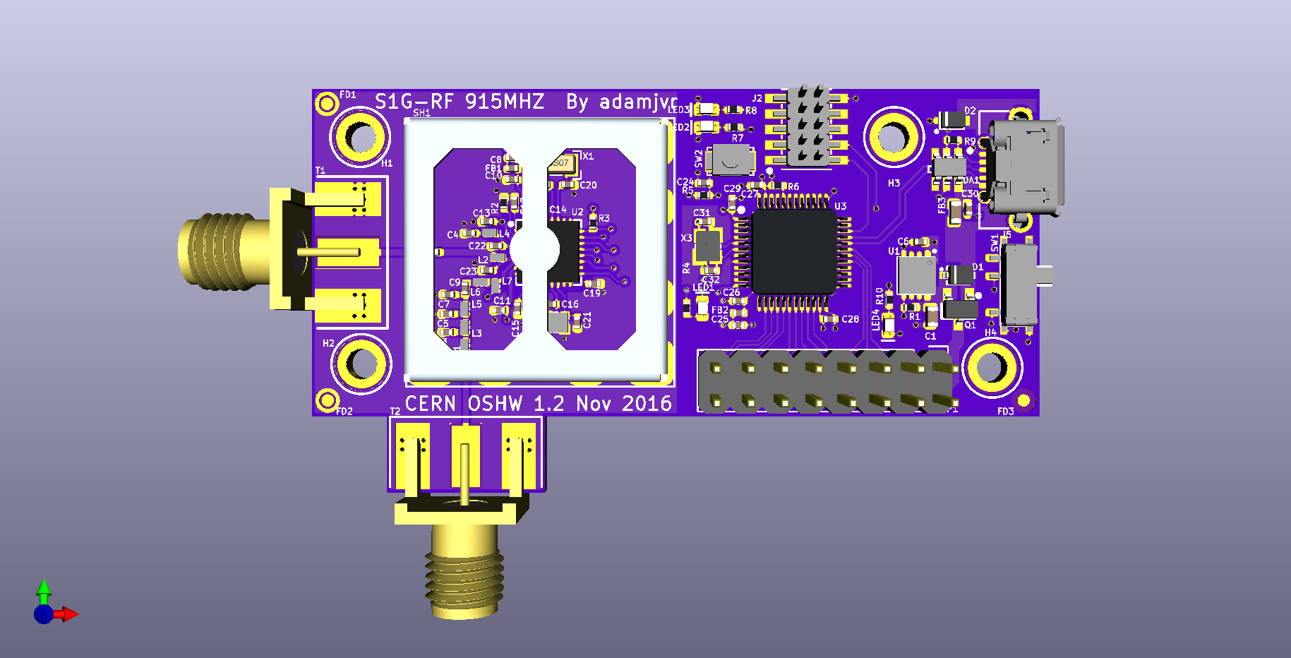
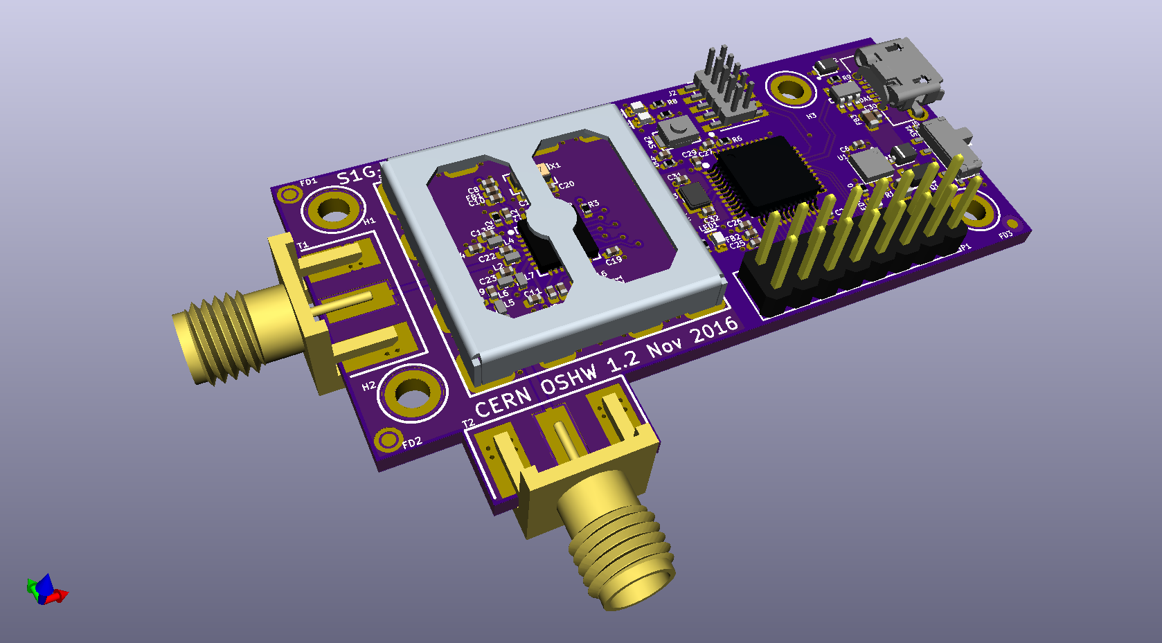
Separate PA/LNA Match Implementation:
2D From KiCAD:
![]()
KiCAD 3D Top Side:
KiCAD 3D Anagled:![]()
So thats the initial first pass on the PCB for both versions of the radio, I'll be reading app notes and tuning these designs quite a bit before I build so stay tuned for updates on what I do and what I'll learn ;)![]()
-
It Starts
11/08/2016 at 02:57 • 0 commentsSo I've been wanting to do this project for a long time, awhile ago myself and a couple friends were interested in long range XBee radios frm Maxstream. The prices were pretty high at the time so we thought about rolling our own PCB for one of the wireless chipset that Maxstream used. Though at the time we had no experience in PCB design let along designing RF PCBs. So after a few years of gaining experience designing all sorts of things, I decided to explore this project again.
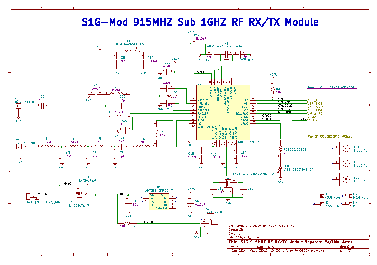
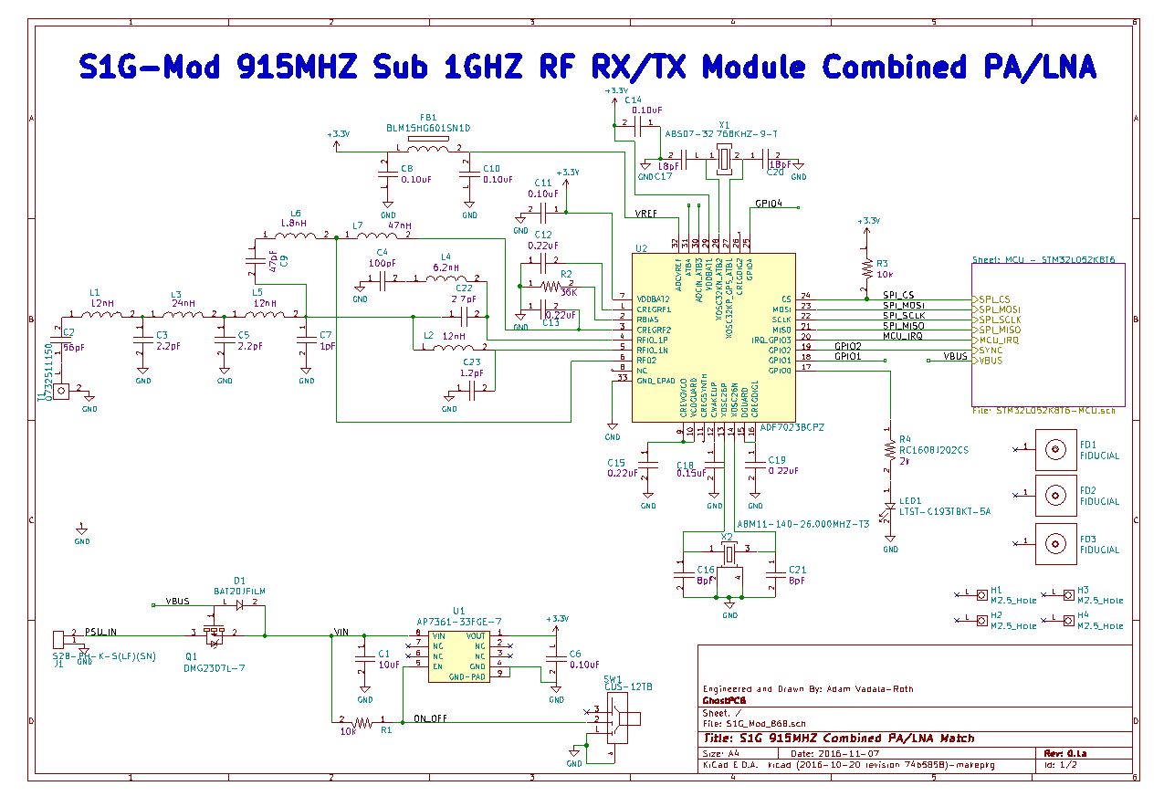
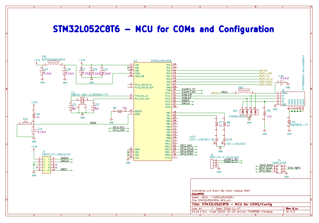
With that I did some searching of RF transceivers and came upon the ADF7023, its a pretty nice chipset and supposedly capable of transmitting at a fairly great distance. The modules I will be developing will essentially be ADF7023 + STM32 ARM Cortex M0+ on a board with SMA antennas, several connection ports, and USB. The RF section is nearly a straight implementation of the reference design but some components have been swapped out for ones with better tolerance and RF grade. The rest of the schematic is orginial to the project. At this point I've created two schematics, one for separate and combined PA/LNA matches. This should let me explore the capabilities of the chipset and allow me to build 4 unique radios, for 433MHZ the baords will be the same but components changed.
Here are the Schematics:
Separate Matches
![]()
Combined Match
![]()
MCU Section, its the same for both boards:
![]()
So that;s where I am at currently, these are subject to change a lot over the course of development, this is my first real RF project as I don't count any of the 2.4GHZ stuff I've done so comment any suggestions if you'd like :) Stay tuned for more!
S1G RF: Sub 1GHZ Radio Modules 915MHZ and 433MHZ
Sub 1GHZ RF wireless modules operating at 915MHZ and 433MHZ ISM bands, based on the ADF7023, full open source!
 AVR
AVR