zaphod
-
Conclusion and Next Steps
08/01/2021 at 18:00 • 0 commentsConclusion:
Overall I'm fairly pleased with how the project turned out. It more or less works, in the sense that its an accurate free running digital clock, and the hardware isn't too hacked together. That being said I think there are a number of things I could have done better:
- improved board design
- improved electrical/mechanical integration
- better parts selection
- better software/firmware
Improved board design:
The biggest issue with the main PCB is that it doesn't have a proper high frequency transmission path to the FPGA for the main time source signal. I initially did this since I was worried about needing to swap FPGA pins during development, and I figured my main time source signal wasn't fast enough to warrant designing proper microstriplines and adding RF connectors. In practice these turned out to be not great assumptions, I didn't really need to shuffle FPGA pins, and a 20MHz square wave is really pushing what you can just send down a normal wire. Hence the hack of adding in an SMA cable to get from the main oscillator to the FPGA.
Furthermore, if I was doing this again I think that I would redesign the PCB to plug right into the display module and thereby get rid of the need for a separate display wiring board, which brings me to the next section:
Improved electrical mechanical integration:
Right now the clock's electronics are spread across 3 circuit boards:
- the main board - a custom PCB
- the OCXO board - a chunk of copper clad board
- the wiring board - a chunk of perf-board
and the display module is separate from the main board/wiring board stack. I think that having the oscillator separate from the main board is reasonable since it allows me to change out the oscillator in the future, however, I think that the wiring board and main board probably should have been combined in to one PCB that just mounted onto the back of the display module. This would have reduced the board count, made the insides a lot neater, and would have made the final design a little smaller. I originally decided to separate the wiring board and the main board since I thought that having a general purpose AVR+FPGA board might be handy, but after all of the nonsense of changing the FPGA part way through due to supply issues I'm not sure that the final board is all that useful as a general purpose thing after all.
I also would've done a PCB for the OCXO if I was doing this again, since that way I could get the SMA connector and microstriplines exactly right.
The final major annoyance is that the AVR programming port is buried under the display wiring board, which just adds more friction to the firmware development process. If I was doing this again I'd certainly try to find a better spot for the programmer.
Better parts selection:
I'm not too unhappy with the parts that I ended up using, since they were informed by the current parts shortage, but if that hadn't been an issue I think that I could've done a better job of picking parts.
The FPGA I used is complete overkill for this project, and was really only selected due to availability. Really I should've used a much smaller FPGA, or also put a softcore mcu on the FPGA in addition to my time counting logic.
Conversely the AVR micro is a little anemic. I mostly picked it since I'm familiar with the tools, but handling 64 bit time stamps in 8 bit C gets old fast. The other obvious fast solution would've been to thrown an ESP32 in there and just do everything in micropython, but that feels like overkill. Probably I should've spent some time looking at 32 bit arm stuff, and learning a new tool chain...
Better software/firmware:
I'm very happy with how well the verilog works, and I think I did a good job designing and simulating everything (I was even able to catch a bug in the simulator!), but the firmware and software are another story.
The firmware on the AVR is functional, but pretty rudimentary. Its basically just one giant thread, and I think it could be made a bit more functional if I added interrupt routines to handle the SPI and UART communications since that would allow me to adjust the clock's displayed time without needing to reset everything. The firmware also doesn't handle daylight savings time right now, which is a pretty big issue since it means that the clock will be resynchronized every 6 months, so I won't really get to watch it accumulate error over time. I think this could be fixed by writing firmware that lets me update the display without a reset, or by figuring out a good way to encode all of the nonsense that is timezones in the clock's firmware.
The software that sets the clock from a host computer is also nothing special. Right now its just a hundred lines of python and could certainly be a lot more sophisticated. But for now I think its good enough.So in conclusion, the clock isn't perfect, but I'm still happy with it. That being said there are some obvious next steps:
Next Steps:
there are a few things I still want to do:
- get timezones worked out so that the clock can be truly perpetual
- add an uninterruptible power supply/battery back up so that the clock can be transported/survive power outages without losing the epoch
- change the oscillator for an atomic source
- build an atomic oscilllator?
Getting timezones working is basically just a software/firmware effort and so it shouldn't be that hard, but we'll see how motivated I am to do pure software...
Adding an uninterruptible power supply would be pretty cool and I have some ideas for this right now, but the question of how much power the clock needs will in large part be determined by its oscillator, so this might have to wait until I figure out a better oscillator.
Changing the OCXO for an ebay surplus rubidium oscillator is what I really want to do next since then I'd finally have an atomic clock, but rubidium oscillators are a little expensive (even as surplus), and could likely be a project on its own just to get powered up and working, which is why I didn't do it as part of the first phase of this project. Additionally, I'd like to spend some more time trying to figure out how to characterize the accuracy of my clock as is, since I don't want to spend the money on a rubidium oscillator, unless I can demonstrate that it actually made the clock better, and really measuring the clock's current accuracy could be a project in and of itself...
One day when I'm smarter and I have a lots of time and money (lol) I want to see if I can build a diy atomic oscillator, since I haven't been able to find anyone else who's done one online. This is starting to be the realm of wishful thinking, so I guess I'll end this project here. -
Updated Case
07/31/2021 at 22:52 • 0 commentsI did a previous project log on the case, and since then some things have changed.
Specifically I've done the following:
- redesigned the top cover now that I know how big the internals are
- designed some feet to allow airflow over the power supply
- put the FreeCAD files up on github: https://github.com/ZakSN/z_1_rtc_mech
- printed all of the parts
The Top Cover
I made two major changes to the top cover, its now taller than I originally anticipated since the wiring boards and SMA cables add some height, and the USB plug hole was redesigned to fit around the SMA cable.
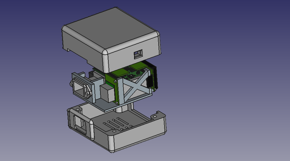
here's the old exploded view showing the USB plug hole:
![]()
and here's a new exploded view showing the modified USB plug hole, and slightly different aspect ratio:
![]()
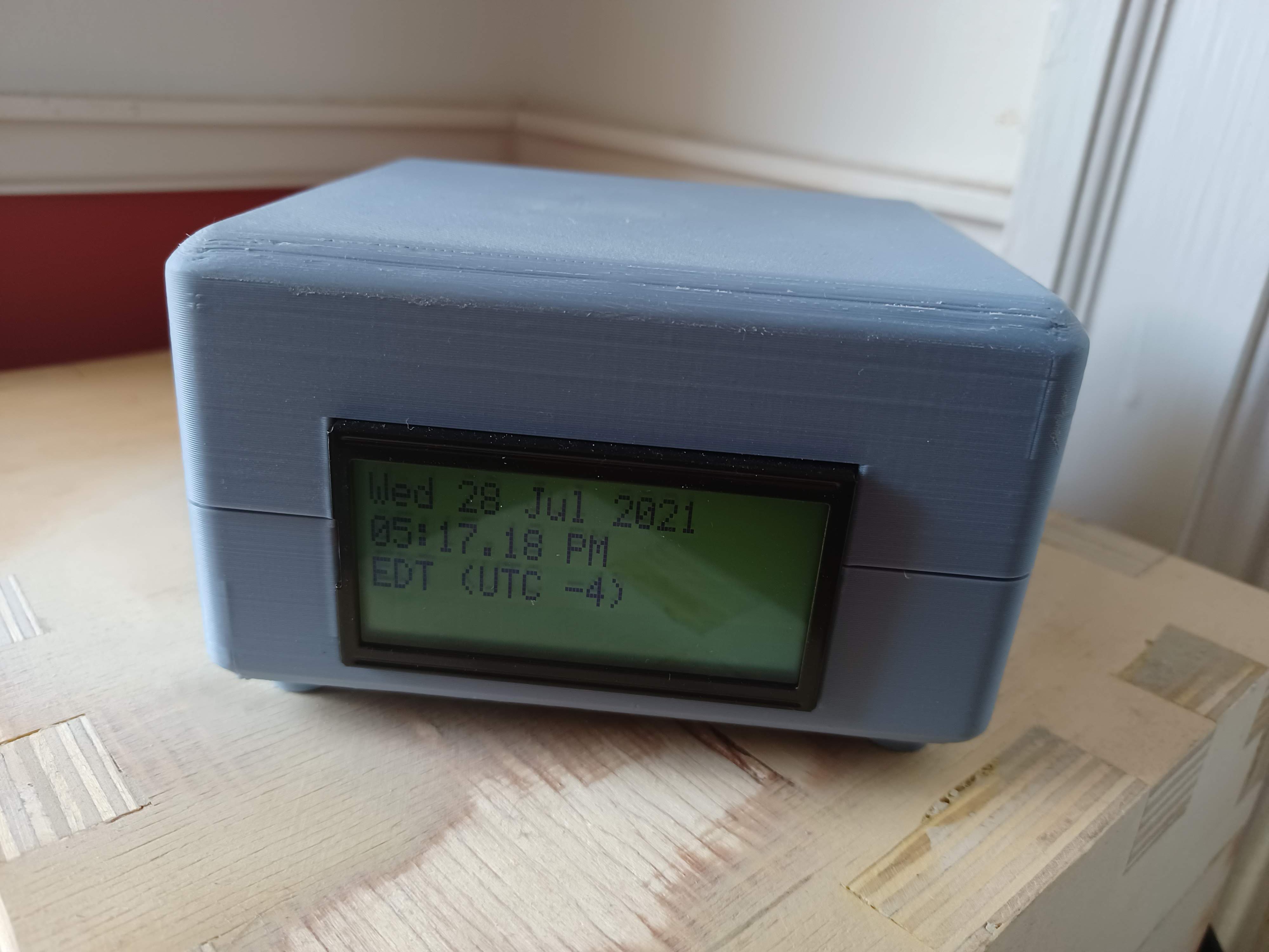
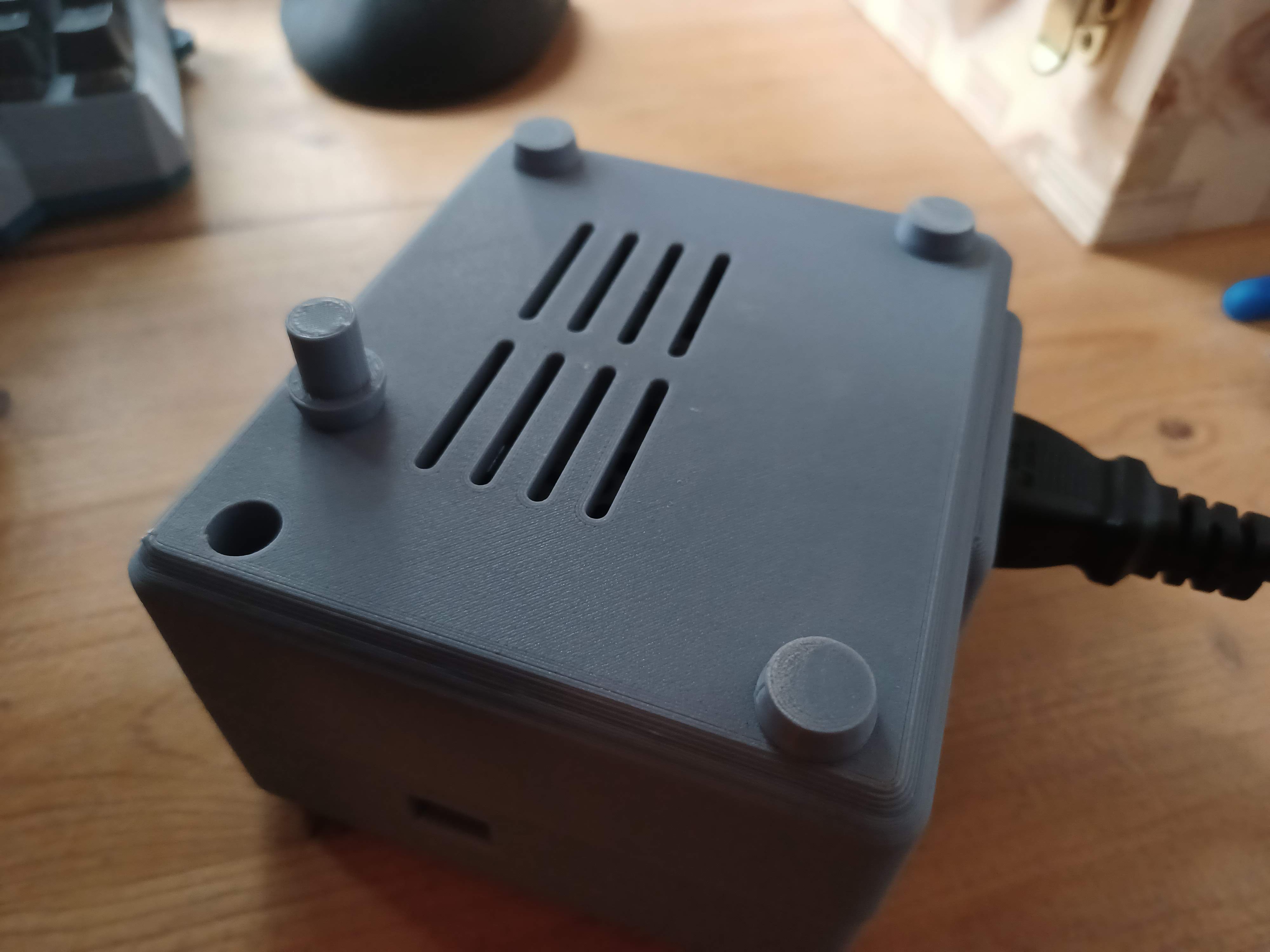
finally here's a few shots of the real case in situ:
![]()
![]()
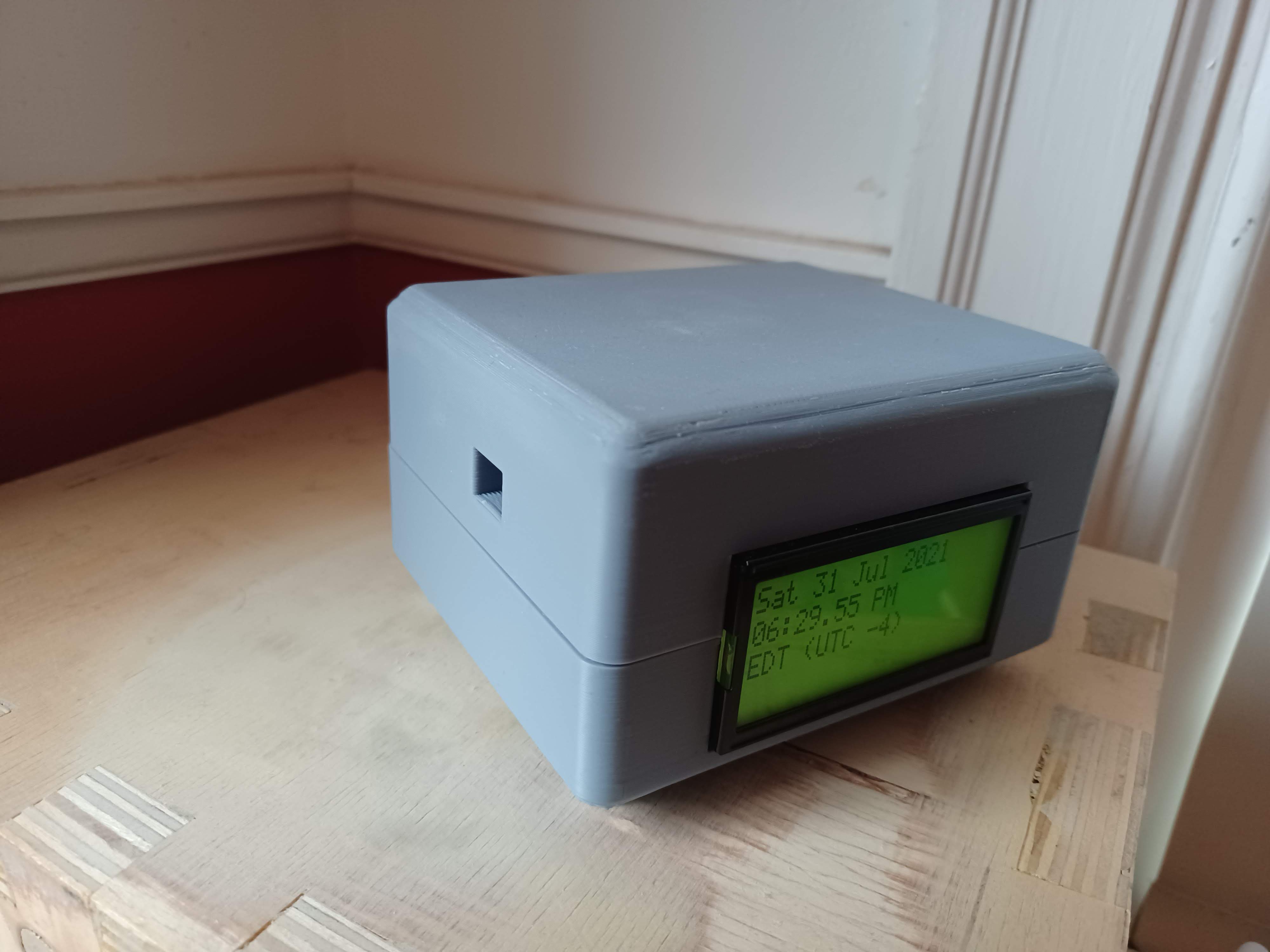
and one of the case removed from the clock so that you can see the inside:
![]()
Note the lug at the back of the case. This is to help retain the midframe near the AC power jack so that nothing bends when you plug/unplug the cable, this feature actually works pretty well.
The threaded inserts and USB plug hole weren't as much of a success. The threaded inserts work ok, but its hard to make them go in square, and as I set them in with my soldering iron they sort of filled up with plastic, hopefully they'll be more durable than just threading into the plastic.
The USB plug hole is a major annoyance, since it's two small and far away from the USB jack on the board and is therefore pretty hard to get a cable to plug in properly. I knew this would be a problem, which is why I originally designed a bigger recess (see image above), but there ended up just not being room for such a large recess once I had the SMA cable installed as well.
The Feet
The clock needed some little feet to raise it up off the surface it sits on so that there would be some airflow through the cooling grille on the bottom of the enclosure. The electronics don't get particularly hot, but I figured a little airflow probably couldn't hurt.
The feet are pretty simple and just friction fit into the bottom of the case (They pry out with a pocket knife for disassembly):
![]()
everything is printed with PLA+ on my Ender 3, with ~0.3mm layer height, 70C bed and 200C nozzle. I don't have gcode or STLs posted anywhere, so if you want the STLs for some reason you'll have to export them out of FreeCAD yourself: https://github.com/ZakSN/z_1_rtc_mech. I did this because I didn't want to maintain up to date STLs in a repo (probably there's a git build hook for this, but oh well).
Whew, that's it for build logs. Next I'll write up a conclusion, next steps post, and I'll try and add an index of these build logs for easier navigation.
-
Squashing Hardware Bugs
07/28/2021 at 22:46 • 0 commentsIn the last project log I mentioned that I encountered some hardware bugs that required solving. They were:
- mechanical strain on the main electrical assembly occasionally caused the display to stop working
- changing the wire that connects the main oscillator to the FPGA results in the clock not ticking any more
Solving problem 1
I initially suspected that this was due to a cold solder somewhere in the connections between the micro and the LCD, but after much reflowing of solder joints and continuity testing I couldn't find the problem.
Eventually, I just started desperately trying to see if any of the LCD data lines were connected to ground by accident, and this actually turned up a result. After some more hunting I found the source of the problem.
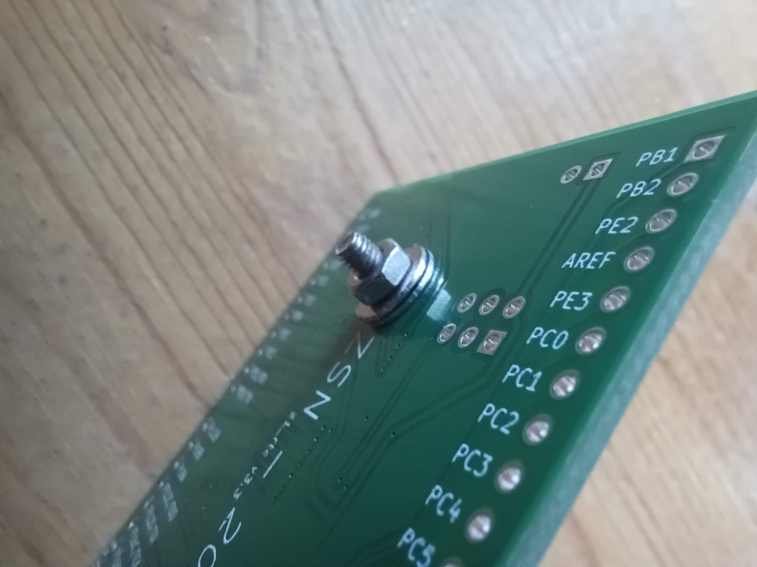
Instead of using proper standoffs I was using a nut and some washers to get the main PCB at the right height off of the power supply as shown in this image:
![]()
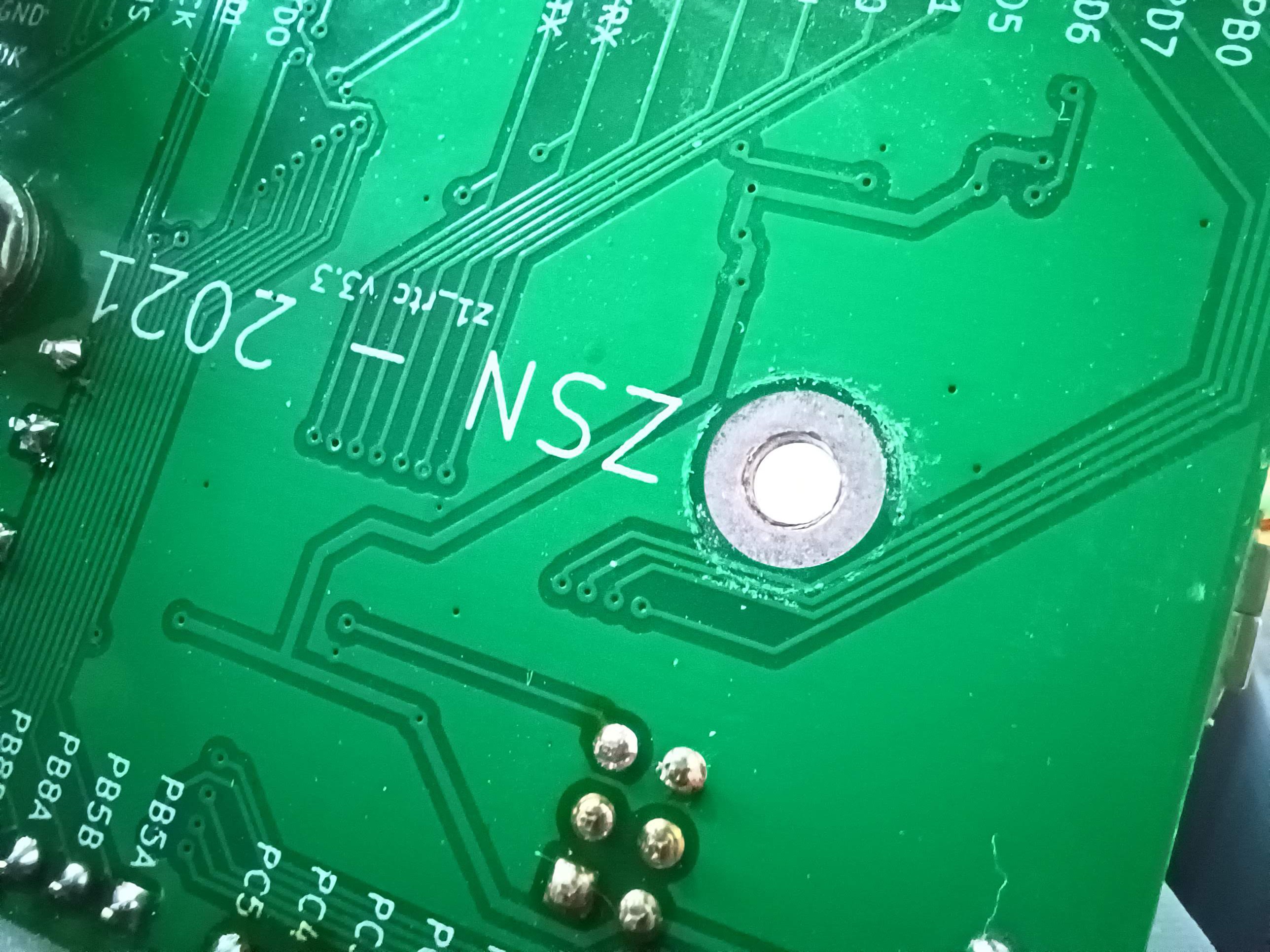
and it turns out that the edge of the washer was slightly sharp and larger than the plating around KiCad's default M3 hole. Furthermore, I had an LCD data line routed next to the mounting hole, and so the washer had cut through the soldermask on both the ground plane and the signal line and managed to just barely bridge the two. here's a picture showing the damaged soldermask where the washer was:
![]()
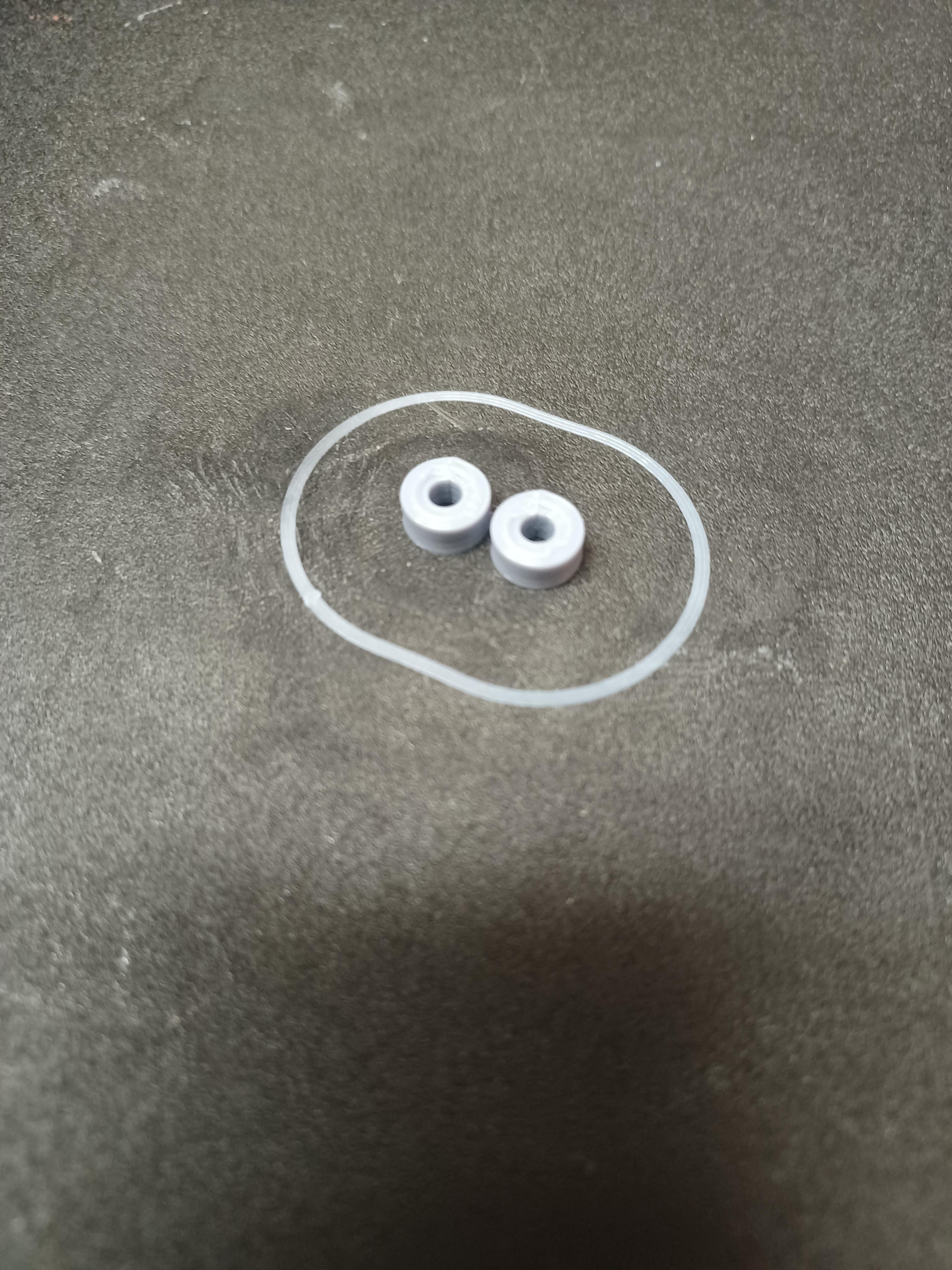
Annoyingly, this bridge was not very stable, and so the error it presented was intermittent and sometimes solved by bending electronics assembly a little, making it seem like the result of a cold solder. Once I'd discovered the source of the bug though the solution was to simply 3d print some appropriately sized standoffs:
![]()
Solving Problem 2:
Problem 2 was a lot worse. Basically I got all of the firmware working while the hardware was in an unfinished state, and part of that unfinished state was that the wire connecting the main crystal to the FPGA was just a random chunk of wire I'd soldered in.
Later when I went to replace the random wire with a shorter piece of wire with headers (to allow the main PCB to be disassembled from the oscillator) the clock stopped ticking.
Fair enough, forcing a 20MHz square wave through some 0.1" headers is probably asking a lot, so I undid the headers and just soldered in a wire, and it still didn't work. So then I went back to the initial long wire, and it also didn't work...
At this point it was clear that there was some transmission line nonsense going on that I do not have the tools to deal with, so I started getting desperate. I tried all sorts of different wires, I tried changing FPGA pins/slew rates, I tried using some shielded cable (cut out of an old USB cord), and basically nothing worked.
During testing I periodically switched back to the initial wire and every once in a while it would work again, but not always. At this point I was worried that the physical structure of the conductors was acting as a resonator or filter or something.
Out of shear desperation I decided to try replacing the 20MHz line with an SMA cable, and connect to the main PCB and the OCXO with proper SMA connectors. In the end this is what ended up working which is great! But also indicated that I really should have done better job of considering my high frequency signal path in the first place, which I mostly neglected since "20MHz isn't that fast". (a 20MHz square wave has some really high freq components though!)
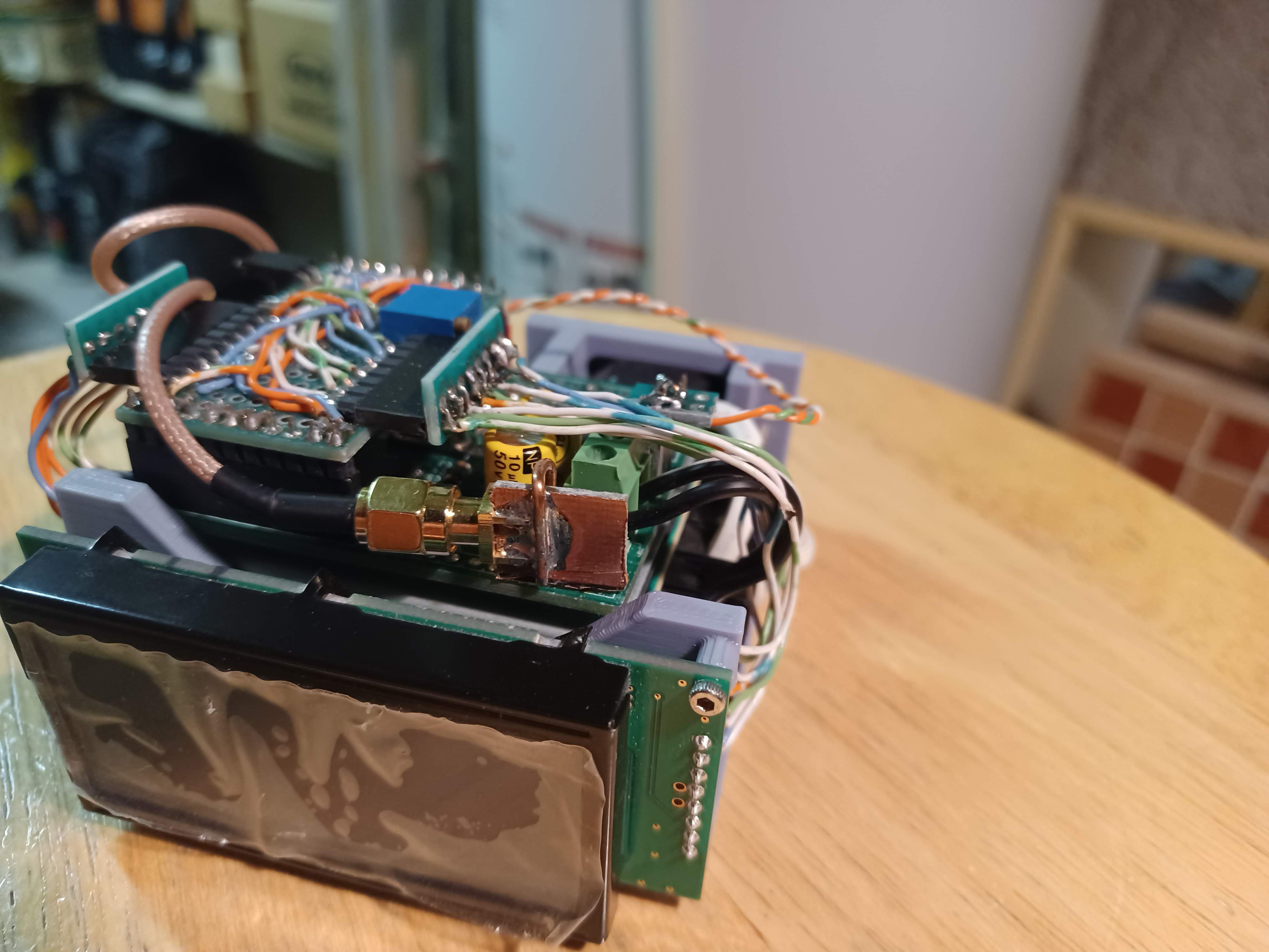
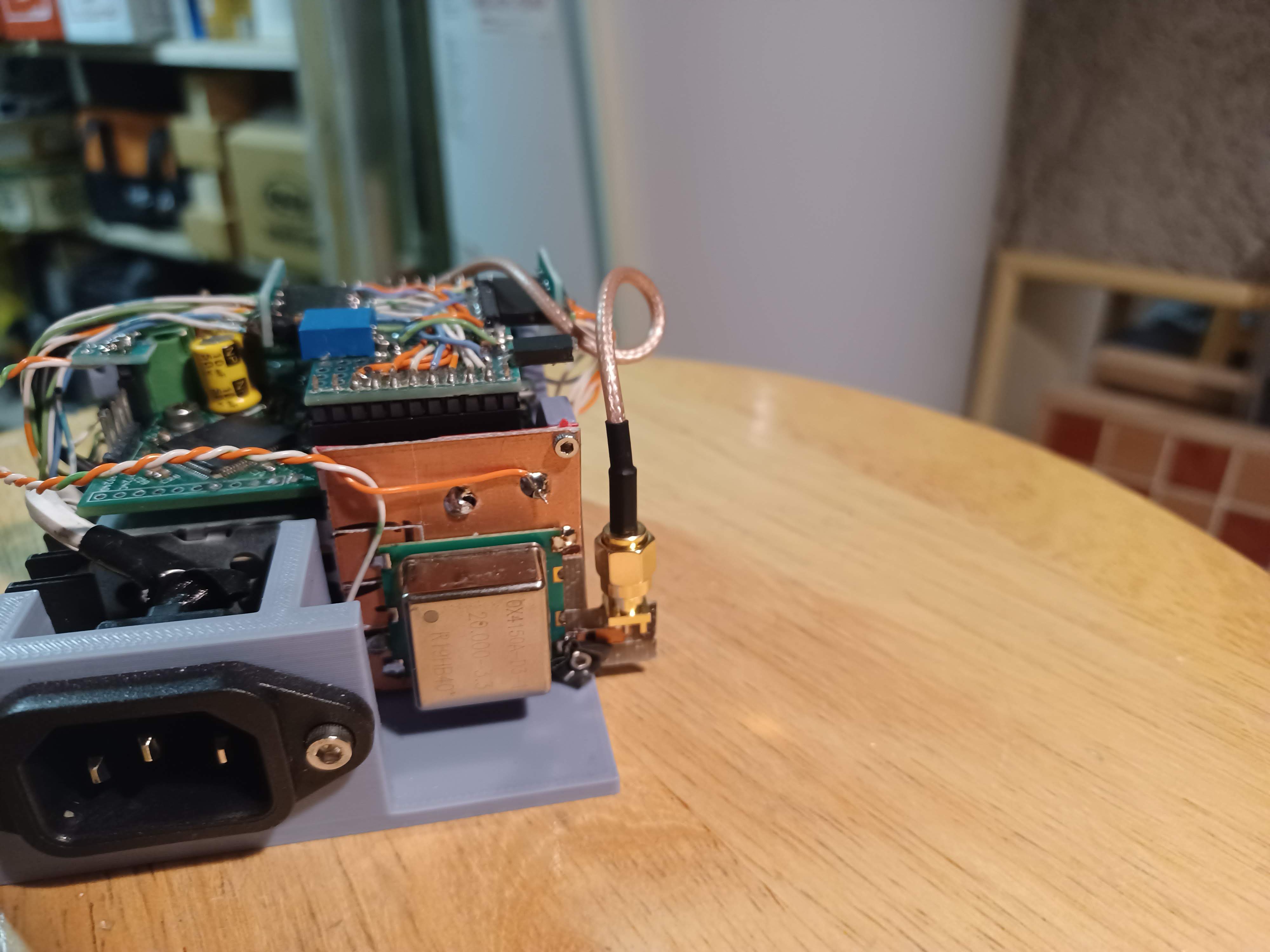
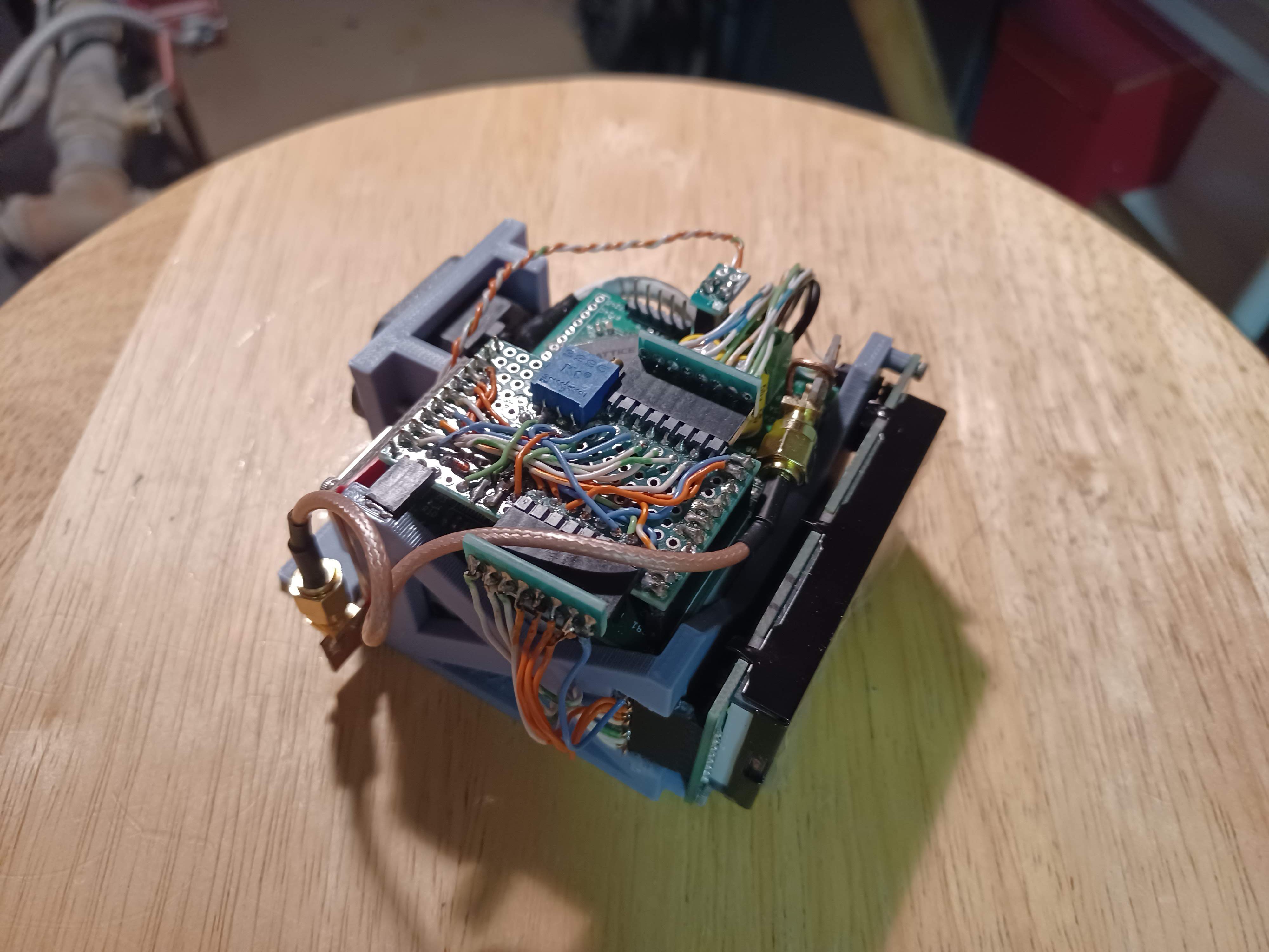
Anyway, In order to get this fix working I needed to build an adapter board that would allow me to hack an SMA jack onto the main PCB, and carrier board for the OCXO that includes an SMA jack. In the end my solution looked like this:
![]()
this figure shows the PCB side connection, the SMA connector is on a small right angle board that connects the signal and ground to the main PCB ![]()
this figure shows the board I made for the OCXO, its just hacked out of copper clad (vaguely dead bug style), and has wires for power, as well as a spot for the other SMA connector ![]()
this figure just shows the whole run of SMA cable As you can see from the images above, its a bit of a hack job, but it does have some retro ham radio/diy rf vibes which makes me feel all warm and fuzzy inside.
also worth mentioning that I did try to cut the tracks that connect to the SMA jacks such that they form 50 Ohm microstrip lines to try and avoid reflections at the SMA jacks, but IDK if it helped much in the end, since the dimensions are just what I could do by hand, and IDK what the impedance of either the OCXO output or the FPGA input is.
-
It lives!
07/28/2021 at 22:03 • 0 commentsA lot has happened since the last project log, specifically I got the firmware into a usable state, wrote some simple scripts for setting the clock, and printed the top cover. This is what it looks like right now:
![]()
In addition to getting the firmware and software in a working state, I also had to hunt down two hardware bugs in order to get the hardware to a point where I'm comfortable calling it done.
As such I'll split up this discussion over a couple of project logs. This log will discuss the firmware and software, and the next log will discuss the hardware bugs I had to fix. I'll also try to write a log discussing the case design since that's changed a little as well.
on to the firmware!
Firmware for this project lives here: https://github.com/ZakSN/z_1_rtc/tree/master/firmware/avr
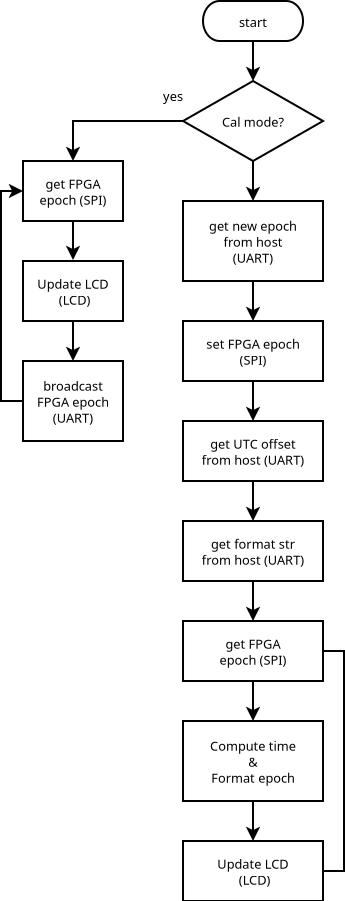
The clock's firmware has a couple of important functions:
- allow a user (via a host computer) to put a new epoch into the fpga's epoch register
- retrieve the current fpga epoch
- calculate the current time from the fpga epoch
- format and display the current time on the device display
additionally the firmware retains a simple mode call 'cal mode' where the fpga epoch register is not reset, and the clock simply broadcasts the current fpga epoch (starting from 0x0 at reset) over uart and to the display.
Ultimately full detail will only come from reading the code in the repo above, but here's a flow chart that explains what the clock's firmware does:
![]()
Basically, 'cal mode' allows me to produce calibration graphs as seen in this project log, and !'cal mode' lets the clock act like a clock.
In !'cal mode' the clock needs some setup information, specifically:- we need to know the current unix epoch (e.g. what time is it?)
- we need to know the current timezone (e.g. how many hours offset from the unix epoch)
- and we need to know how to format the time for the display
all of this information is provided to the clock via a simple python script that basically just checks the computer's clock for NTP time information and then blasts bits at the clock over UART.
Internally the clock uses the avr gcc `time.h` lib to do time calculation. This works pretty well, but has a couple of quirks due to running in an embedded environment:
- avr gcc uses a different (smaller) epoch, so I have to convert the FPGA (64 bit unix) epoch to an avr epoch
- daylight savings time/timezones don't work (the timezone database is too huge for embedded apps and so the avr gcc implementation of `time.h` just doesn't deal with timezones)
to get around the timezone thing I just embed the current timezone in the display format. This at least lets the clock display the current timezone as e.g. 'EDT (UTC -4)', but it means that the clock needs to be reset when ever daylight savings time changes occur, which while not ideal is acceptable.
I think that's everything I want to say about the firmware/software for the clock. As usual its probably more informative to just go and read the code in the repo if you really care about how this thing works for some reason...
-
ticking accurately
07/12/2021 at 20:45 • 0 commentsIn the last update I got the clock ticking, but it was not doing so accurately (I was able to notice it lose a half hour over the course of a couple days), and the firmware/verilog running on it was a bit of a mess
the first order of business was cleaning up the code repo. This was just some organization and some simple changes to the verilog top level to get it to work on the new FPGA. As part of this clean up I added UART support to the device's firmware, so now it blasts the number of seconds since it was powered up (I call this the clock's epoch (i.e. like the unix epoch)) out over the UART. I also added a software directory and some host side python scripts to allow me to calibrate the clock.
Specifically I wrote two scripts:
- z_1_rtc_host.py
- plot_error.py
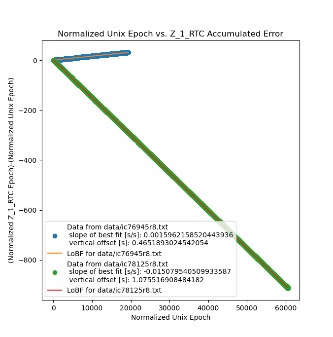
z_1_rtc_host.py counts the number of seconds that the clock has accumulated or lost since the program was started. It works by comparing the clock's internal epoch to the unix time stamp reported by my computer (since the clock starts at 0 when you power it up the script normalizes both time stamps to the t=0 being the time that the program started). The output of the script is just a simple .csv with one column showing how long the measurement has been running for, and the other showing how many seconds the clock has lost (negative number), or accumulated (positive number).plot_error.py just plots the .csv file with the number of seconds (according to my computer) that the experiment ran for as the independent variable. With no tuning I got a graph that looked like this:
![]()
no tuning, after running for ~60kSec This image is mostly pretty bad, after ~60kSec the clock was ~900Sec slow, or in other words it lost about 15 minutes in only 16.66 hours, which is far from usable. This is a deviation of about 1.5%. That being said, the graph is very linear, which means that the observed error is systematic, and can therefore be calibrated out, at least in theory.
I went ahead and calculated a corrected master frequency based on the slope of the line in the last image, and replaced the nominal OCXO master frequency with the calculated OCXO master frequency in the main divider module, and reran the experiment:
![]()
green is before tuning, and blue is after tuning Obviously this is a lot better, but not perfect. Now the clock is running ~0.15% fast, so in the ~22kSec I ran the second experiment for the clock still manged to pick up ~33Sec, or about half a minute in just over 6 hours. Still not usable. While the observed error is still linear, and can therefore be corrected for I figured that it was probably indicating an underlying flaw in the verilog responsible for counting the pulses coming from the master oscillator.
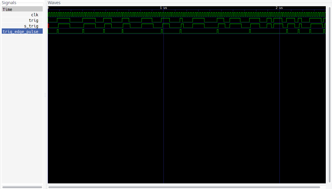
So, after some messing around I went back to my initial simulations and was able to spot a doozy of a bug. IDK how I missed it the first time around, but here it is:![]()
this is the output of the divider test bench (link), showing the signals responsible for synchronizing the master oscillator to the FPGA's internal clock, and then producing a single clock pulse that can be used to increment the counting logic. Basically trig is the master oscillator, and trig_edge_pulse should be a one FPGA clock pulse that corresponds to the rising edge of the master oscillator, however, if you look just before the 1us (and 2us) mark you can see that trig_edge_pulse is missing a master oscillator edge! this is bad news!
(notes:- the simulation time base is arbitrary, so 1us is not a real time
- the simulation shows trig as irregular, and clk (as well as all clk referenced signals) as regular, in practice this is reversed, the FPGA clk is irregular and the master oscillator is regular, but writing simulations with an irregular clk is annoying.
)
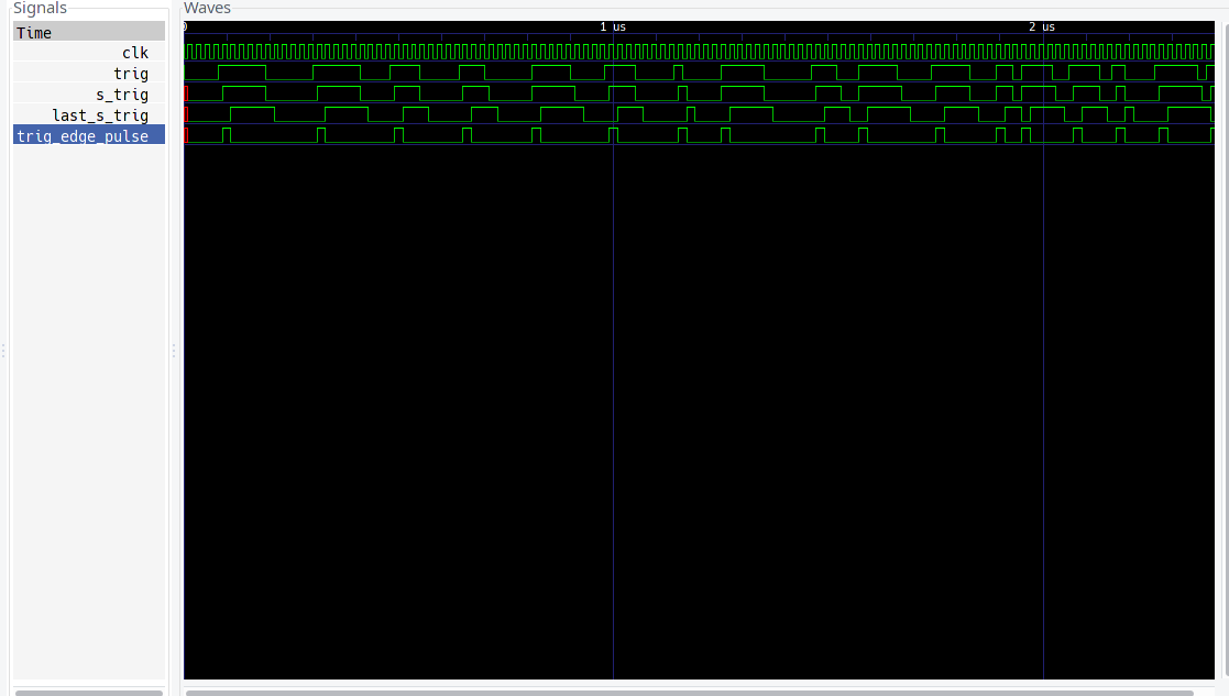
It seems like the error occurs only when the the external trigger coincides with the rising edge of the FPGA clk. Thus the solution was to add another synchronization step as follows:![]()
here we see that there is a trig_edge_pulse on every rising edge of the trigger signal!
But the real proof of a squashed bug is in the real world, so here's a measurement with the patched verilog and the initial values for divider frequency:

and as you can see the clock is dead on accurate. In ~80kSec it did not gain or lose a single second, which is almost a whole day without any observable error!
Unfortunately, this means that I'm going to have a hard time telling just how accurate the clock actually is, unless I want to take a really long measurement. For example, the accuracy I'm trying to beat is +/- 1sec/30day (what Casio rates most of their wristwatches to), or ~3.85e-7. In practical terms this means that I would have to run the clock for at least a month continuously in order to observe any error since I can only measure to a precision of one second. This is compounded by the fact that my computer clock, despite being synchronized to NTP, will inevitably have some error and if it is on the order of 1 sec/month then I may not be able to observe any error in my clock. Thus in order to get a reliable measurement demonstrating accuracy better than 1sec/month I would have to run an experiment for much longer than a month. Or, I need more than 1 second precision in my measurement setup.
Nonetheless, these are very encouraging results. They demonstrate that the clock is certainly 'usabely accurate', and is quite likely as good as or better than 1sec/month.Notes:
some notes that didn't fit into the rest of the post.
first note:
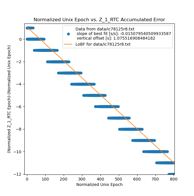
since the process of comparing the unix timestamp to the clock is not synchronized with the clock's ticking you can sometimes get +/- 1 sec of observed instantaneous error, e.g:
- computer checks unix time stamp, gets value of 1000, which is what the clock is displaying,
- clock ticks over, and displays value of 1001
- computer checks clock time stamp, gets value of 1001 (meanwhile the unix time stamp has rolled over at somepoint)
- calculates error as 1001-1000=+1 sec
the upshot of this is that as the clock drifts the graphs show overlaping regions of error, that appear as a thick line in the zoomed out graphs above. If you zoom on them in it looks like this:
![]()
that's also why the calculated slope of the error after I fixed the bug was something on the order of 5e-8 instead of just 0 (as discussed above, my setup wasn't running long enough to detect errors of this magnitude)
second note:
the maximum theoretical accuracy for the clock is limited by the accuracy of the crystal. Part number: OX4150A-D3-1-20.000-3.3-7. Naively adding freq calibration and stability numbers (ignoring aging), gives a number of +\- 107ppb or 1.07e-7 or a little under four times better than a Casio watch. In practice, probably only about as good as a Casio watch. -
It ticks! for real this time!
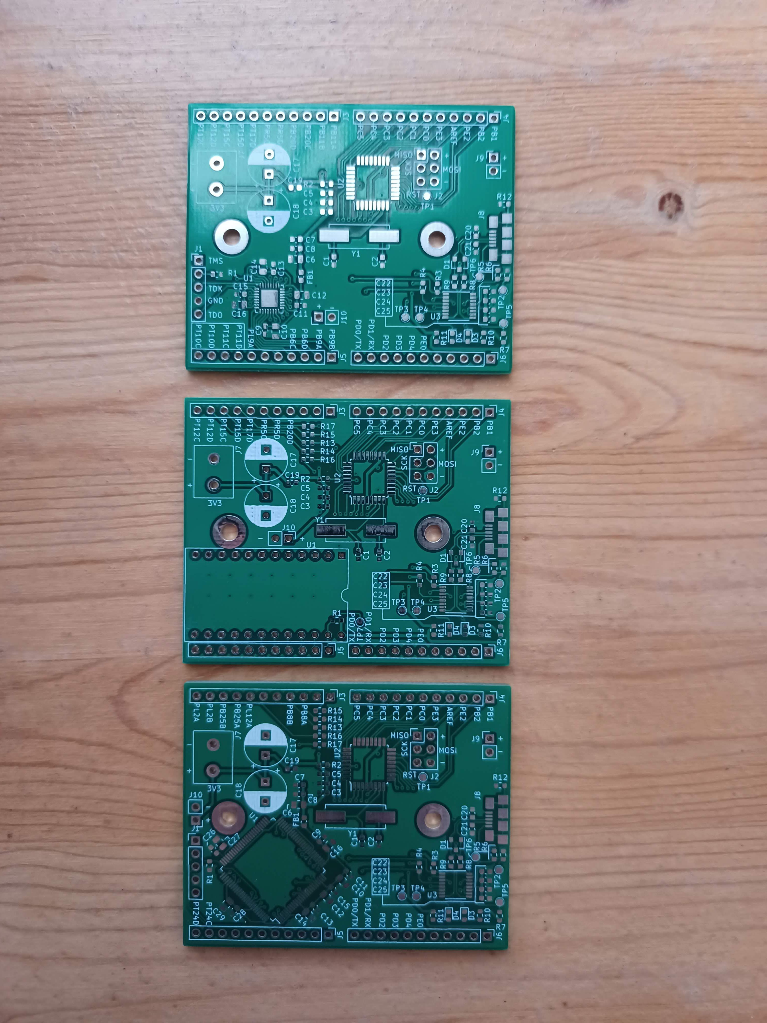
07/04/2021 at 22:30 • 0 commentsin my last post I described the new revisions to the main PCB. They have arrived and I've successfully populated a v3.3 board.
here's a comparison shot of all 3 versions of the PCB:
![]()
from top to bottom we have: v3.1, v3.2, and v3.3.
Basically everything is identical across all three version except the FPGA, v3.1 is designed to work with a 32QFN lmcxo2-1200hc part (the same as in the tinyFPGA Ax1), v3.2 is designed to include an entire tinyFPGA board, and v3.3 uses a 100TQFP lmcxo2-2000hc part.
As you'll recall I was unable to order more of the 1200hc parts and so I had to switch to the 2000hc part, which is unfortunately an order of magnitude more than I really need, but its at least in stock, and a package that I can solder. I basically designed the v3.2 as as back up in case the v3.3 didn't work, so I started bringup with the v3.3.
Assembly of the v3.3 board was pretty straightforward. Since the micro and FTDI circuits were exactly the same, they went together no problem. I did run out of capacitors though, and had to harvest some 0603 0.1uF from an old v1 board. Soldering on the 100TQFP was a pain, since I don't have a proper hot air station, but I got there in the end, all though I spent a lot of time hunting down and individually reflowing bad solders. I also had a nasty intermittently disconnected cold solder on one of the headers that attaches the main board to the display interconnect board, that took a long time to hunt down (I even ended up replacing the micro before figuring out that the intermittancy was due to a bad solder joint, and not a blown micro).
Since I all ready had test code ready to go I was able to confirm that the micro and FTDI chip were up an running pretty quickly. Getting the FPGA configured took some more effort though.
I'm using the tinyFPGA programmer for all of this, which is a little ten dollar USB->JTAG bridge with some software that's designed to make it go with the tinyFPGA Ax1 and Ax2 boards. However, the lmcxo2-2000hc-5tg100i is not one of the chips that is used on the Ax1 and Ax2 boards. I was hoping that it would just work out of the box anyway, but I was not so lucky.
I briefly considered getting the official Lattice JTAG programming cable, but its like $230, and even ebay clones are ~$30. Thus the only cost effective solution was to take a hack at the tinyFPGA programmer software: https://github.com/tinyfpga/TinyFPGA-Programmer-Application
From what I can see the tinyFPGA programming software consists of 3 major parts:
- the firmware on the PIC microcontroller located on the programming adapter. I didn't touch this, but I think its conceptually pretty simple: all it does is present a serial port to the host and manipulate some GPIO according to commands from the host. I don't think it even knows about the JTAG protocol, which I think is all handled by the host, but don't quote me on that.
- a python command line interface for talking to the serial port presented by the programming adapter. I think this cmd interface is technically human usable, but I always use the gui. This is the part that knows the JTAG protocol, and how to parse *.JED files.
- finally a little python gui that talks to the cmd interface and handle's some niceties like file picking and warning you when a programming file has been updated on the disk (link to this above)
The code base for the gui seems pretty stable, based on the github page, while the cmd interface seems to have had some more work done on it (the gui submodules an old version of the cmd interface).
To make a long story short, the reason that the gui wasn't programming my chip is that once it identifies an adapter it checks the IDCODE of the device that you're trying to program. IDCODEs uniquely identify the part number, and the programmer lets you configure the target if the IDCODE matches the chip used in the tinyFPGA Ax1 or Ax2. After some digging (page 187 of this: https://media.digikey.com/pdf/Data%20Sheets/Lattice%20PDFs/MachX02%20Family%20Handbook.pd ) I was able to figure out the IDOCODE of the lmcxo2-2000hc-5tg100i, and then add it to the list of known/acceptable devices. I was half expecting to need to do some more hacking, but once It could identify the attached device everything else just worked, and so my whole patch was like five lines:
diff --git a/tinyfpga-programmer-gui.py b/tinyfpga-programmer-gui.py
old mode 100644
new mode 100755
index f3a0f3e..254c539
--- a/tinyfpga-programmer-gui.py
+++ b/tinyfpga-programmer-gui.py
@@ -169,7 +169,6 @@ class TinyFPGAASeries(ProgrammerHardwareAdapter):

             def status_callback(status):
                 global port_success
-
                 if status == [0x43, 0x80, 0x2B, 0x01]:
                     com_port_status_sv.set("Connected to TinyFPGA A1. Ready to program.")
                     port_success = True
@@ -178,6 +177,12 @@ class TinyFPGAASeries(ProgrammerHardwareAdapter):
                     com_port_status_sv.set("Connected to TinyFPGA A2. Ready to program.")
                     port_success = True

+                # https://media.digikey.com/pdf/Data%20Sheets/Lattice%20PDFs/MachX02%20Family%20Handbook.pdf
+                # page 187
+               elif status == [0x43, 0xB0, 0x2B, 0x01]:
+                    com_port_status_sv.set("Connected to MachXO2-2000HC device. Ready to program, maybe...")
+                   port_success = True
+
                 else:
                     com_port_status_sv.set("Cannot identify FPGA.  Please ensure proper FPGA power and JTAG connection.")
                     port_success = False
the above goes in this file: https://github.com/tinyfpga/TinyFPGA-Programmer-Application/blob/master/tinyfpga-programmer-gui.py
(in retrospect I probably could have just short circuited the IDCODE check logic and saved my self digging up the datasheet with IDCODES in it, but this is marginally less ugly...)
also shout out to @Luke Valenty for making all of the tinyFPGA stuff open source (and cheap)!
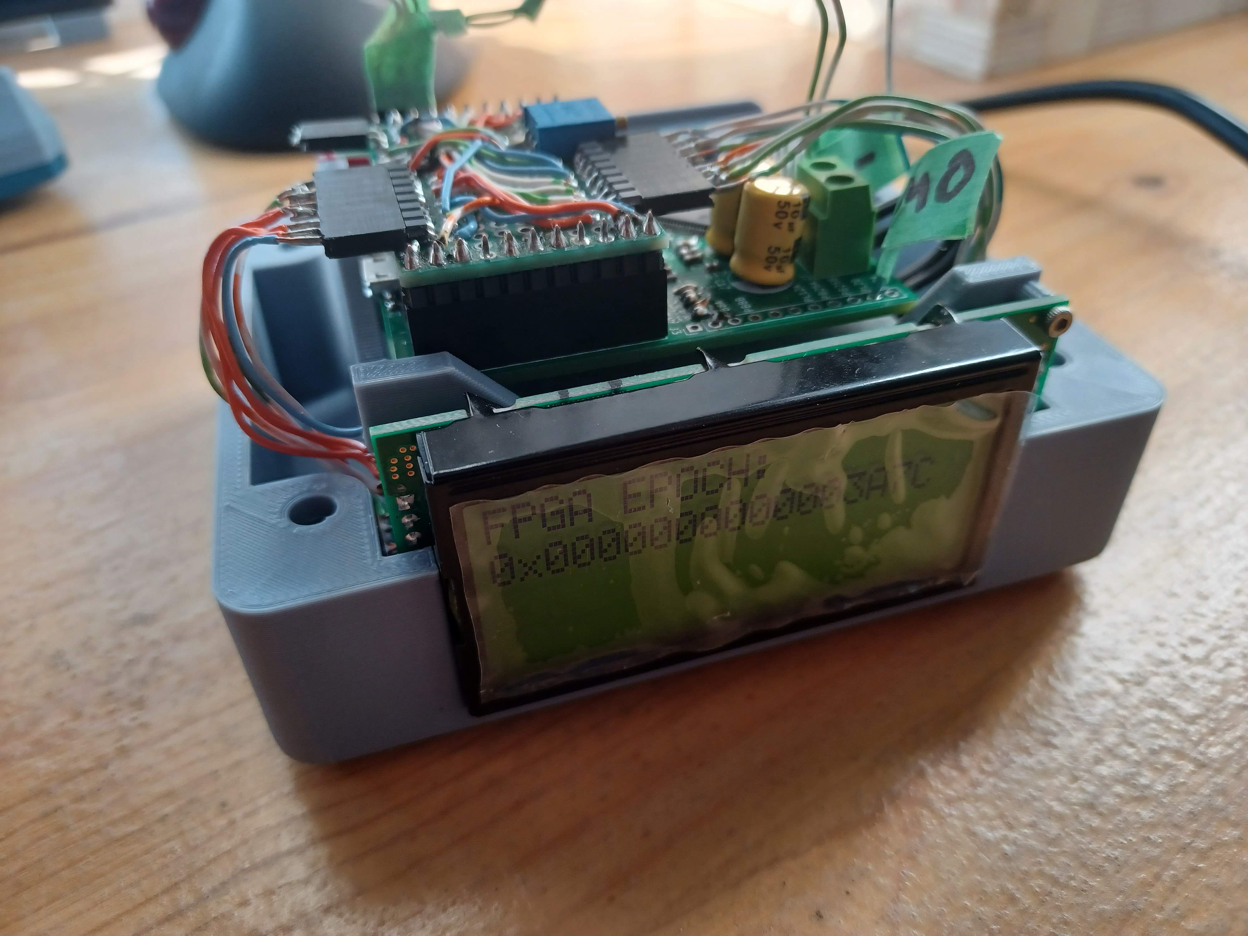
Thus, with all of the chips on my board working it was time to dump in my test code/fpga logic. As you'll recall from the last time I got it ticking things were mostly working but the main counter in the FPGA was occasionally rolling back to 0x0 when it shouldn't have. This time there were no such glitches and its been ticking on my desk for 0x3A7C (14972) seconds, or about 249 minutes and 32 seconds:
![]()
As a bonus that's even pretty accurate! I haven't done a careful accuracy measurement, so I wouldn't know its drifting unless it started missing minutes, but even so I'm pretty pleased, since this is the longest that I've run it from the OCXO, so I'm gald to see that it might be usablely accurate.
The final concern I have is that my FPGA logic just started miraculously working once I switched parts. I have a couple theories about this:
- the old lmcxo2-1200hc part I was using was pretty beatup and maybe about to die (I do think that I zapped one of the I/o at some point, so the rest of the chip might be sort of cooked too)
- the new part is a higher speed grade, and this means my sloppy logic works better since the new chip deals with the incoming master frequency better. This seems the most likely and implies that I ought to redesign the FPGA logic (or at least shuffle pins around to get the master freq on a high speed net)
- lucky routing on the FPGA, this also seems possible and I guess I'll find out when I try to change the verilog...
at any rate the next steps are:
- clean up all of the software/verilog and make sure everything is working
- do a careful check of the overall system accuracy, and hunt down all of the sources of error I can
- write all of the business logic to display a real time (not just a time stamp), as well as all of the set reset logic
- possibly write a client to set the clock to NTP over the serial port
but that's all "just software" (tm)
-
New PCB versions
06/21/2021 at 21:35 • 0 commentsAs mentioned in a previous post the current version (v3.1) of the clock's main PCB didn't work completely. Specifically it caused the FPGA to burn up shortly after being plugged in. This was a pretty mysterious problem, since the FPGA didn't blow immediately, but instead seemed to work for a few minutes (I was even able to configure it once) before starting to draw a lot of current and burning out.
The problem was further compounded by the fact that the particular part number I had specc'd is on back order everywhere, and as a result I was unable to order more parts and do more testing. Additionally the parts I was initially testing with were in unknown condition, since they were originally bought for/built into the first hardware version that I started over a year ago, and hadn't been stored very carefully in the interim. Finally, it's possible that the flux I used during assembly was dodgy (all though this may just be paranoia).
Therefore it's time for some new board revisions.
Before starting on the next version I had to validate as much of the existing design as I could. I was quickly able to get the ATmega up and get it displaying stuff on the display thanks to some old code I had from the first pass at the project. I was also able to confirm that the ATmega ought to be able to talk to my verilog, provided I could get it running on a non-exploded FPGA. This was mostly covered in this log.
The final thing to validate was the FTDI UART/USB bridge. In the original (v1.0) design I had trouble getting the FTDI chip to survive for very long, likely due to a lack of USB protection, and so I had never written code to test bidirectional serial comms.
Fortunately the USB protection on the v3.1 board seems to be sufficient, and I was able to hack together some test code to confirm that I can send bits to the ATmega, and it can send bits back to me. (no picture here since it would just be a screengrab of `minicom` or `cu`).
Thus, I felt ready to begin designing new PCBs. Ideally, the device would use the LMCXO2-1200HC-4SG32C, which is exactly the FPGA in the tinyFPGA Ax2 devboard. Unfortunately the 1200HC is sold out everywhere, and so I needed an alternative. There are two obvious options
- embed a whole tinyFPGA Ax2 devboard
- find a similar part that is still in stock and redesign around it
Option 1 is obviously simpler and quicker, but doesn't give me the nerd-cred of having successfully embedded an FPGA on a PCB I've designed. Option 2 is certainly the hard road, but also presents a better learning opportunity (and maybe a better resume item :) )
At any rate it wasn't a clear decision, and so I decided to just do both options 1 and 2. Which takes a little longer, but doesn't cost much more since JLCPCB lets you batch PCB orders. Thus, option 1 became PCB v3.2, and option 2 became PCB v3.3.
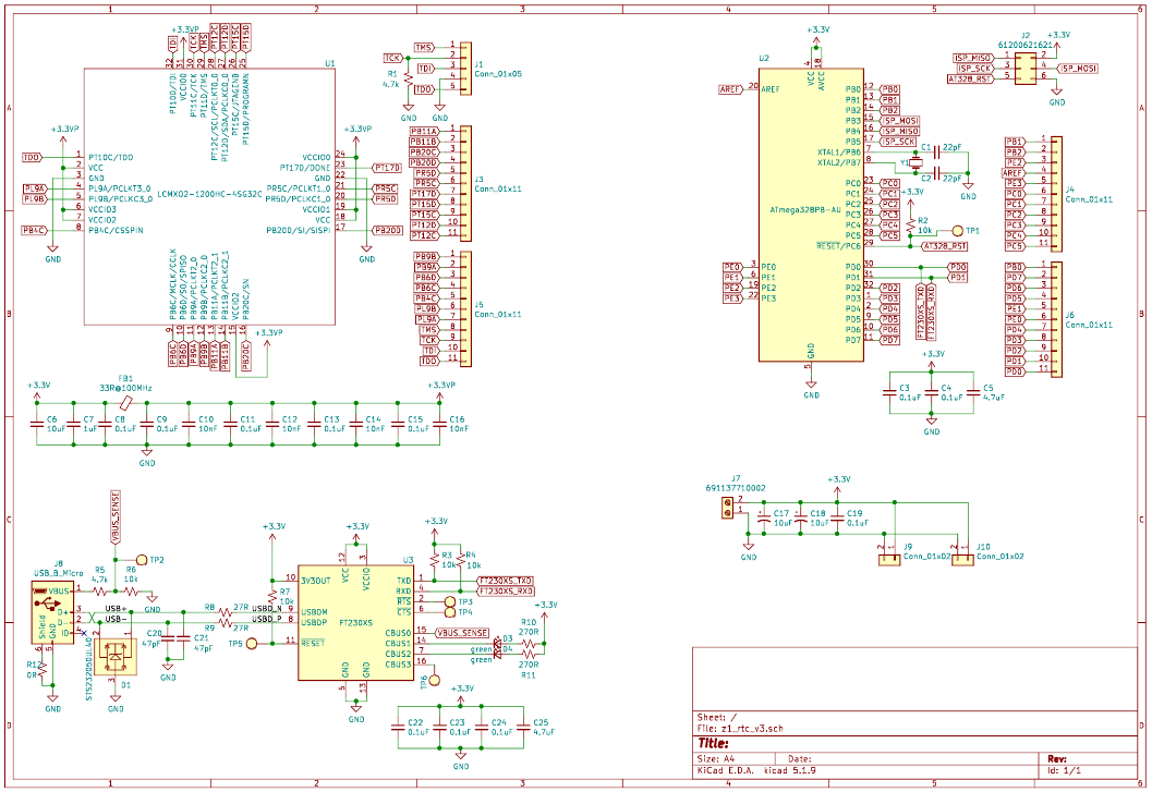
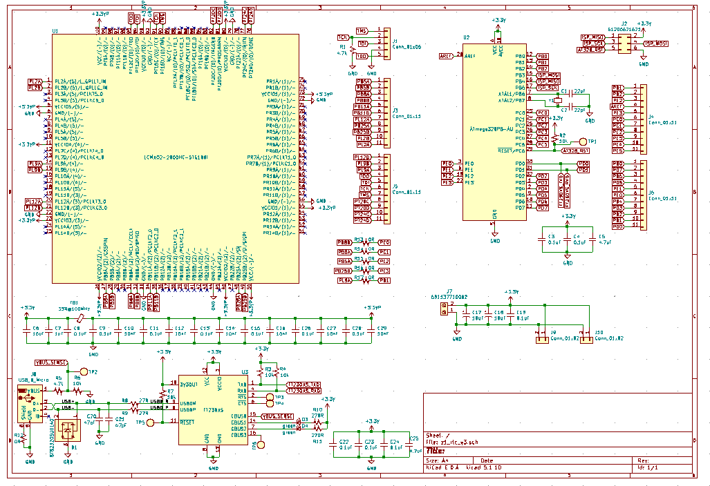
As a refresher this is the schematic for v3.1:
![]()
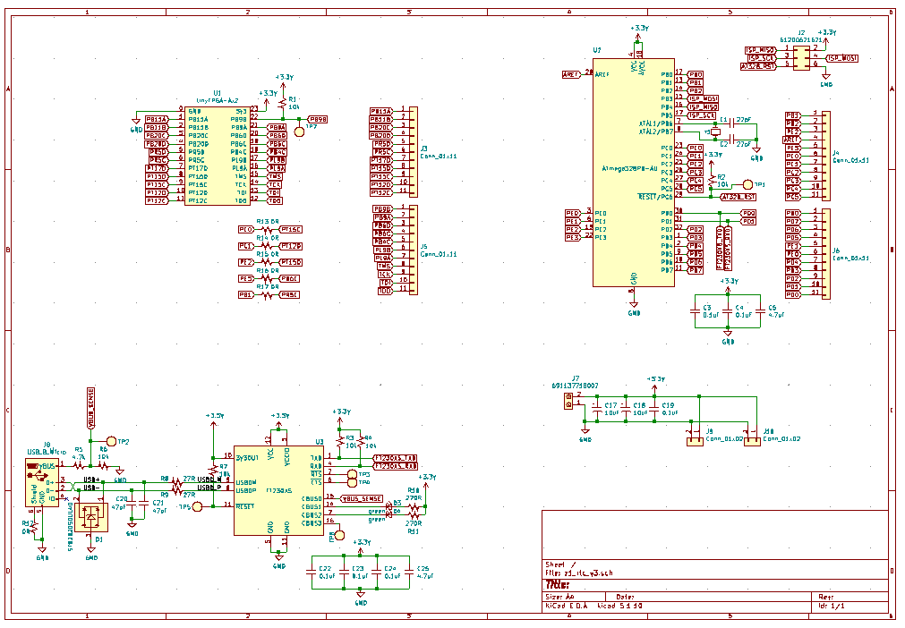
and this is the schematic for v3.2:
![]()
as you can see the v3.2 is a pretty simple replacement of the FPGA+support circuitry with the tinyFPGA-Ax2 module. The only other difference is the bank of 0R jumpers that are used to optionally connect some signals from the micro to the FPGA. Originally I had intended to just use the breakout pins to connect the micro and the FPGA, but the jumpers were easy to add, and will make the final design look a little neater.
For the v3.3 I needed to pick a chip I could actually order. After scraping through digikey and mouser, the cheapest (when considering shipping cost) similar chip I could order was the LCMXO2-2000HC-5TG100I, which is almost the same as the LCMXO2-1200HC-4SG32C, with a couple key differences:
- 2000 LUTs instead of 1200 (I was nowhere near topping out the 1200HC version, so this is pure overhead)
- TFQP-100 package instead of the QFN-32 (waaaaay more io than I'll ever need, but slightly easier to solder down I guess)
- a different speed grade, (series 5, instead of 4, rated for (I)ndustrial, instead of (C)onsumer use)
basically the new chip is complete overkill for what I need, costs like twice as much, and comes in a giant '90s style TFQP with a bazillion pins, but, I was able to buy it this year.
Thus, with my new parts in hand I went ahead and designed v3.3:![]()
which is the same as v3.2 except with an FPGA and the associated support circuitry instead of the module. There will certainly be some sweat and tears required to get my verilog setup and running on the new FPGA, but hopefully it won't be too bad, and if it doesn't work I can always fallback on the v3.2 design.
After some quick layout I went ahead and ordered the boards from JLCPCB, and they should be here in a couple weeks.
If you're interested in finding all of the flaws in boards that I've already paid money for the designs are up on github here: https://github.com/ZakSN/z_1_rtc_pcb, there's a branch for each of v3.1, v3.2, v3.3 (see the readme).
As I mentioned in the last project log, the current FPGA design doesn't really work properly, there's a lot of things that it could be, but I suspect that its also a lot more complicated than it needs to be, and so I plan to try and audit the logic design while I wait for boards to arrive. I may also post a log explaining how the logic currently works, since I'll need to refigure it out anyway.
-
It ticks! (sort of)
06/04/2021 at 23:05 • 0 commentsAs mentioned in a previous project log, there's something up (idk what) with the FPGA circuit on the clock's main board and I fried my last two FPGAs. Unfortunately the Lattice part I had designed around is no longer available so I can't debug the current version of the board.
My plan is to redesign the PCB around a slightly different Lattice FPGA that is still in stock, but first I wanted to confirm that I have a minimum viable FPGA configuration and minimum viable firmware for the micro.
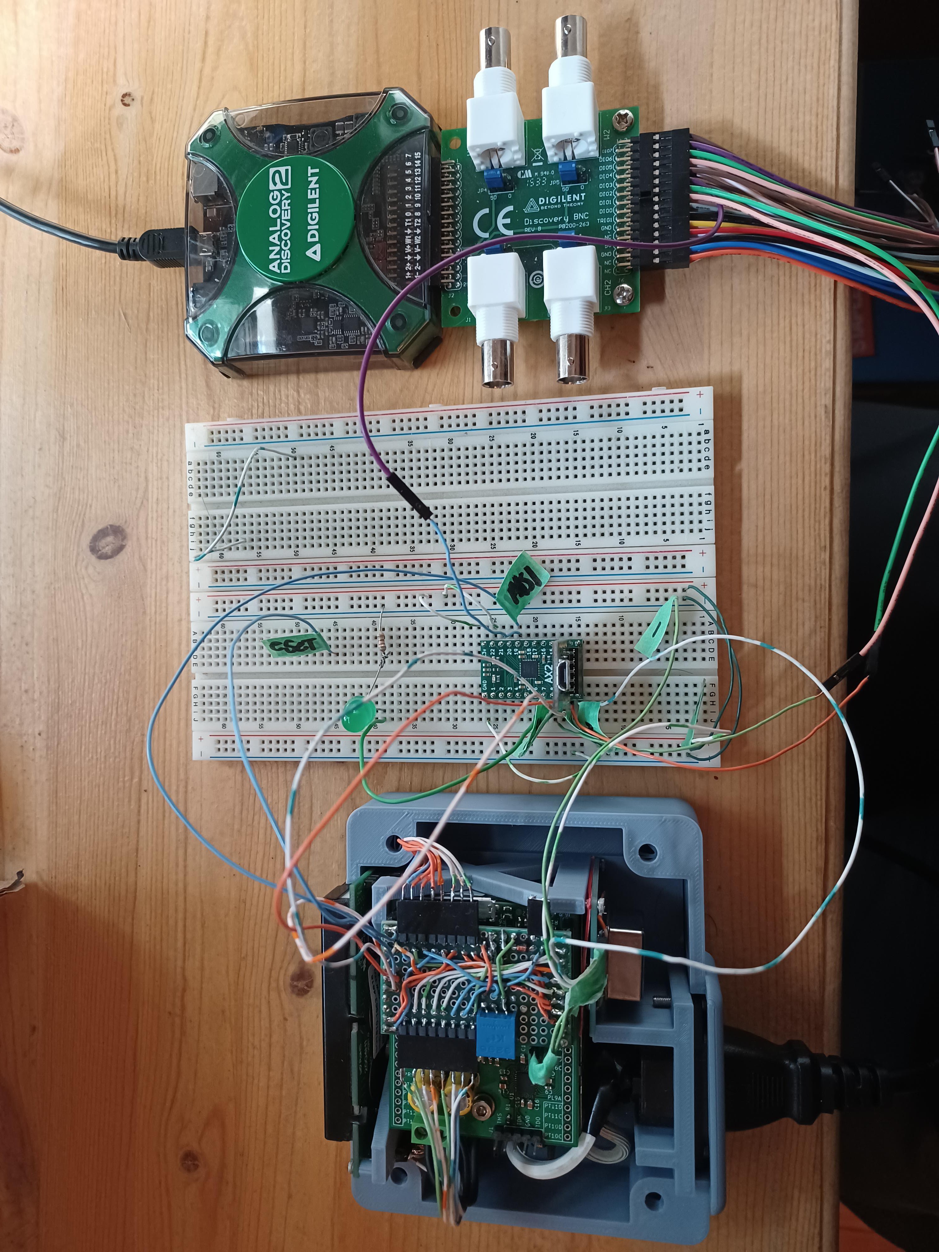
I had developed some example code and a mostly working FPGA config the last time I was working on this project so it was mostly a case of wiring in my TinyFPGA dev board in place of the busted FPGA on the PCB and uploading all of my test code. The hardware setup looks like this:
![]()
top to bottom: USB scope/logic analyzer (analog discovery 2), breadboard with tinyFPGA devboard, the rest of the clock In the setup above the tinyFPGA devboard (on the breadboard) is counting pulses from the master oscillator (silver can near the AC plug in the image above), dividing the master frequency down to 1Hz, and then incrementing an epoch register every second. The ATmega (in the clock on the PCB) just periodically polls the FPGA for the current value in the epoch register over SPI, and then throws that value up on the display. So this test setup confirms the following:
- the FPGA is able to divide a signal down to 1Hz
- the FPGA is able to increment a register and communicate this value over SPI (SPI FSM works)
- the micro is able to update the display
- the micro is able to communicate over SPI with the FPGA
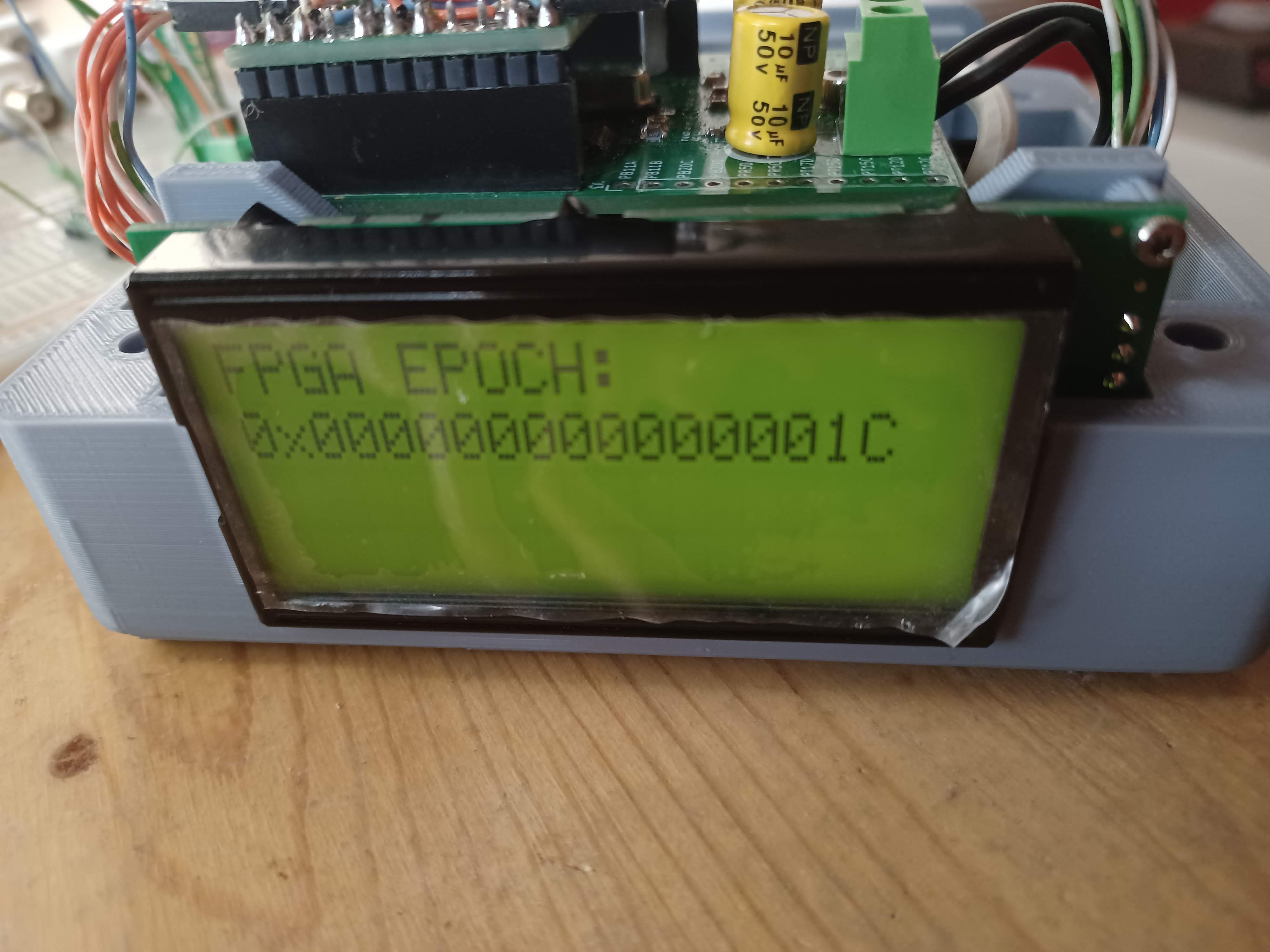
As the image below demonstrates, this was mostly a success:
![]()
here the clock is showing that the FPGA has counted 64'h1C (?'d28) seconds since the clock was turned on. Since the master frequency is 20MHz this means that the FPGA has counted 28*20 = 560 million edges, and reported this over a spi connection.
In theory all of the code/logic to do this all ready existed in a working state from the last time I was working on this project, but it took a while to remember how it all went together. (mysteriously I also had interrupts misconfigured in the 'good' version of the code, which took way too long to debug). But this means that we have a known starting point to begin working on changing the FPGA to a part that is actually available, which is what the next couple of project logs will discuss.
As you probably guessed from the title of this post, dear reader, there is some qualification to the success described above. And that is that the clock is really really inaccurate right now, and the FPGA occasionally loses the state of the epoch register and rolls over to 0x0 prematurely.
There is an obvious problem with the above setup that certainly contributes to (and may be the source of) the above problem; that is that the 20MHz master frequency signal is being dumped right into a breadboard in order to connect to the tinyFPGA. This is suboptimal to say the least. Hopefully a shorter more direct connection between the OCXO and the FPGA will reduce parasitic capacitences and improve the accuracy a little. However there are still other possible sources of error:
- the OCXO's real frequency is not its nominal frequency and this will introduce a systematic error in the epoch count.
- I'm not worried about this though because it should be easy to calibrate out
- I also don't think that this is the primary source of the error that I'm observing
- more likely something is wrong with the logic in the FPGA
- it could be missing edges from the master oscillator (contributes to poor accuracy)
- it is likely also missing some edges on internal signals and therefore rolling over when it shouldn't, its not clear which logic block this is occuring in, (could be the divider or the epoch counter), but this would potentially explain the poor accuracy and the premature roll over that is observed
- this is a more pernicious problem, and will likely require some deeper FPGA magic to resolve...
despite these qualifications, I'm still happy with the state of the project. Right now my focus is on getting a different FPGA integrated into the system, and getting back to this state, but with an FPGA that I can actually source, which is what I'll blog about next. After that we can work on hunting down all of the sources of error in the clock.
-
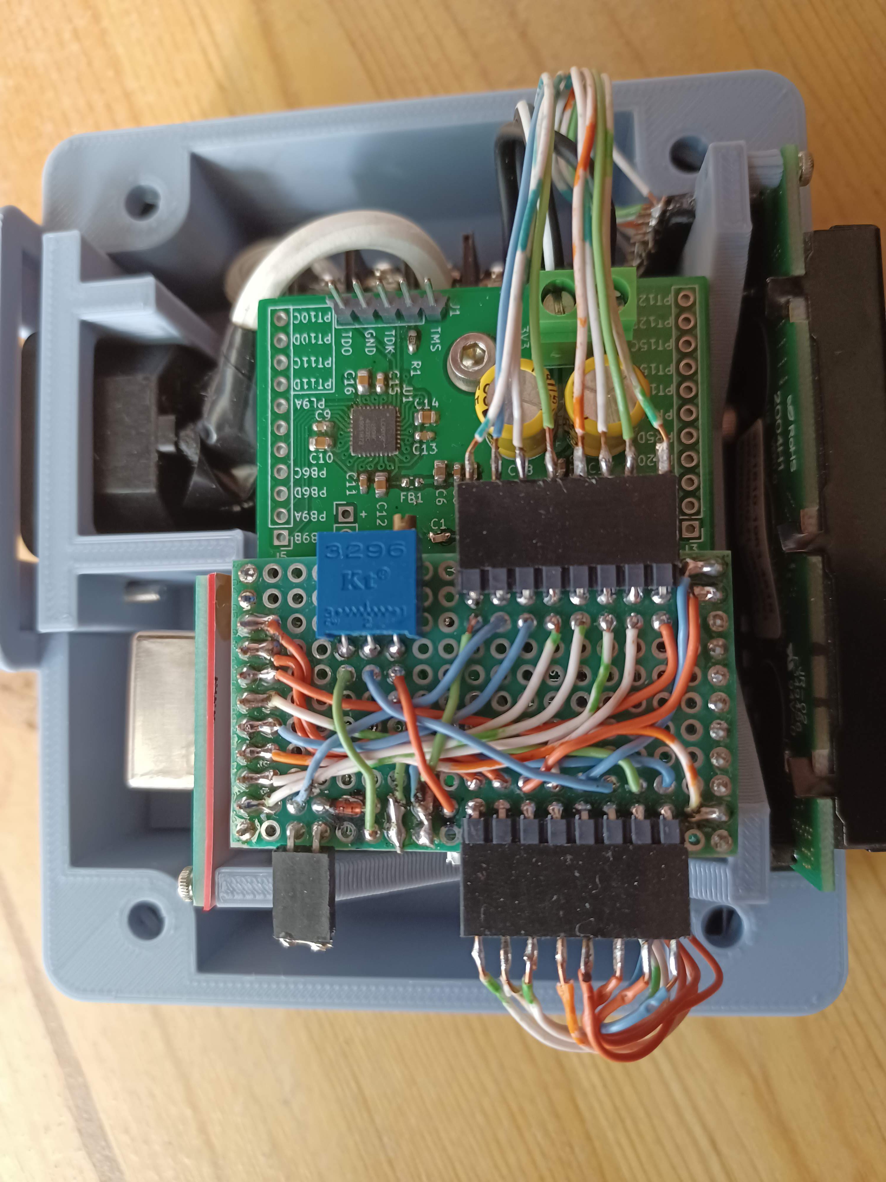
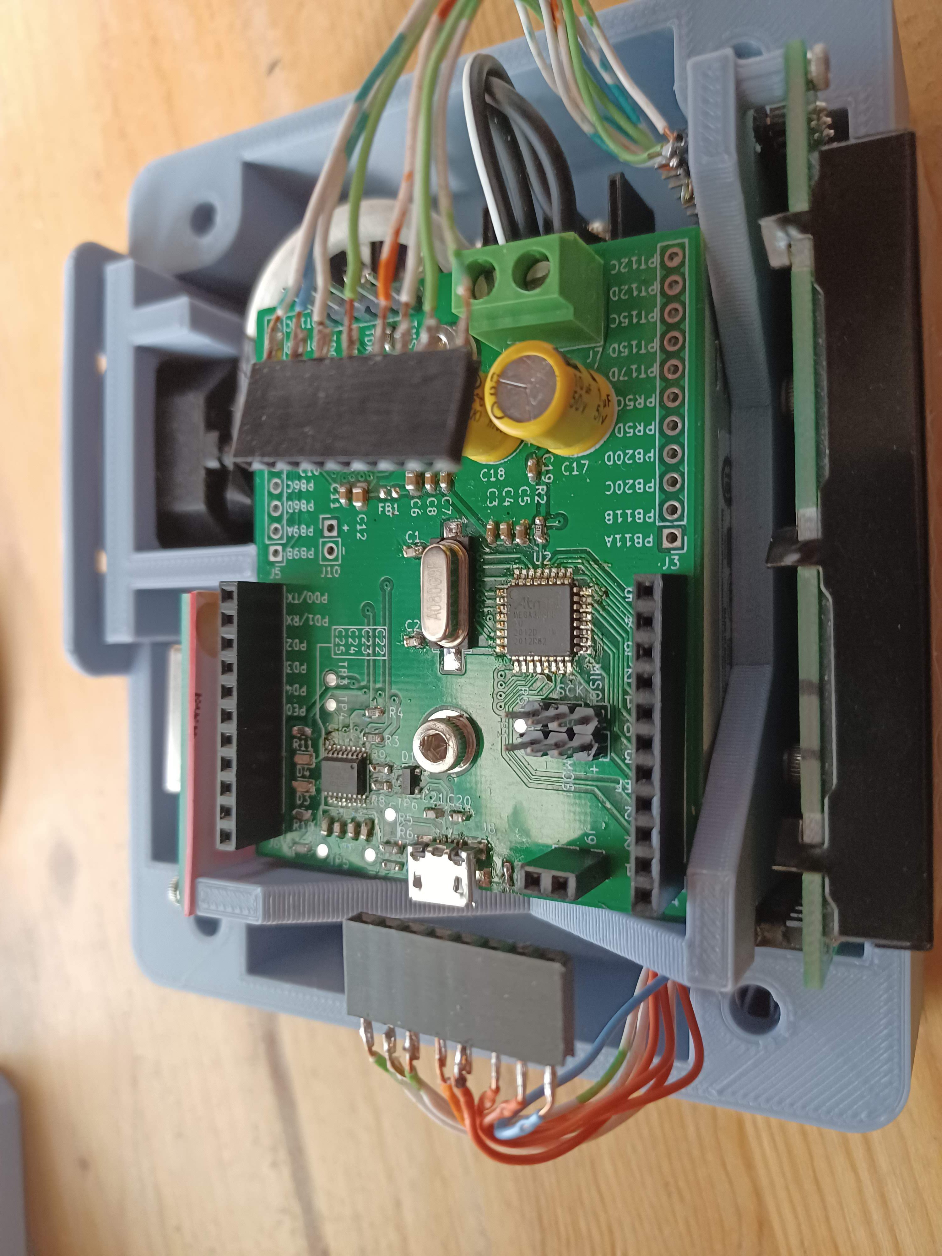
The Display Interconnect Board
05/27/2021 at 21:13 • 0 commentsThe display (this is the exact part used) is on the front of the clock and the main PCB is deep inside, and so some wiring needs to happen.
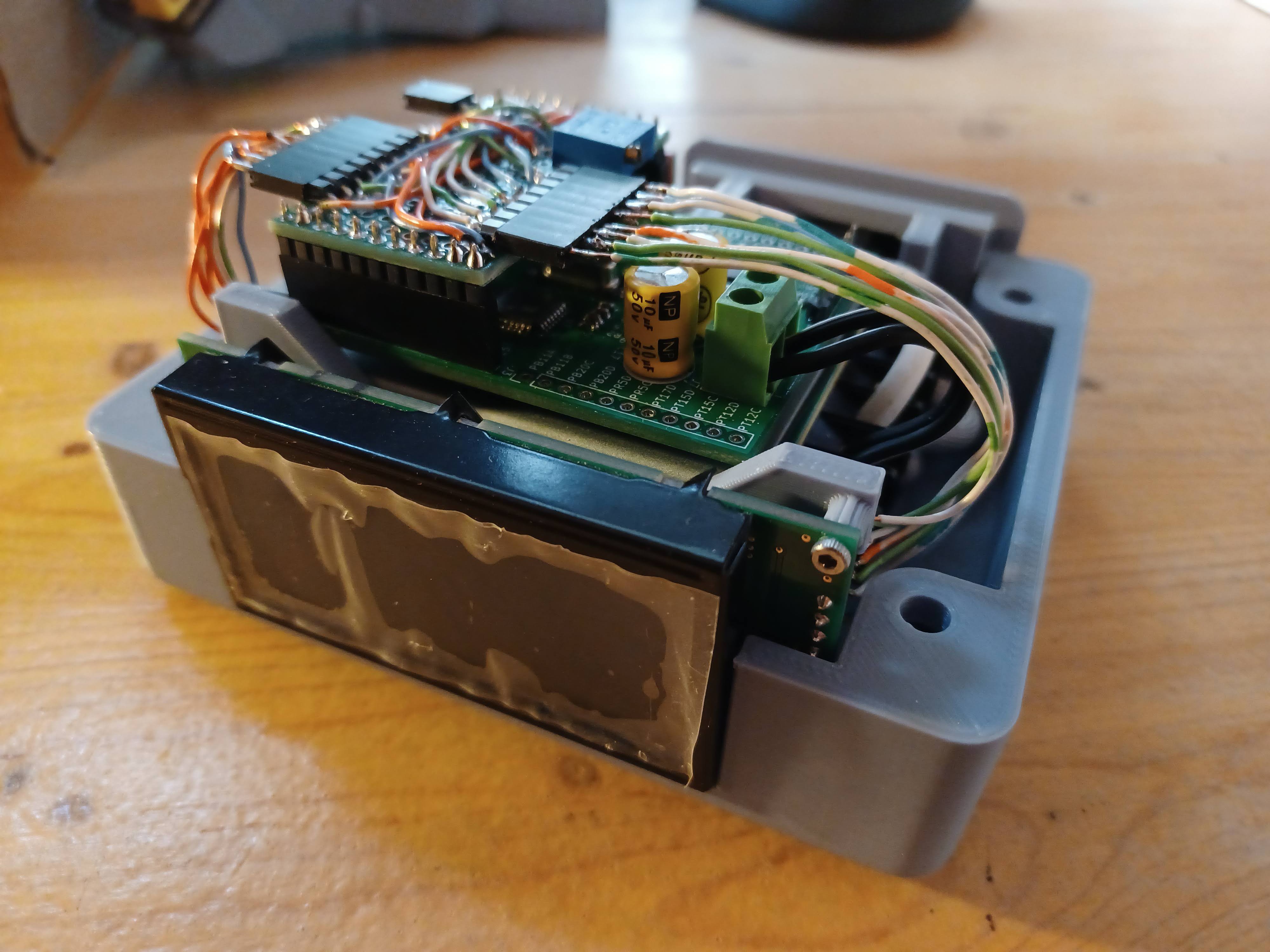
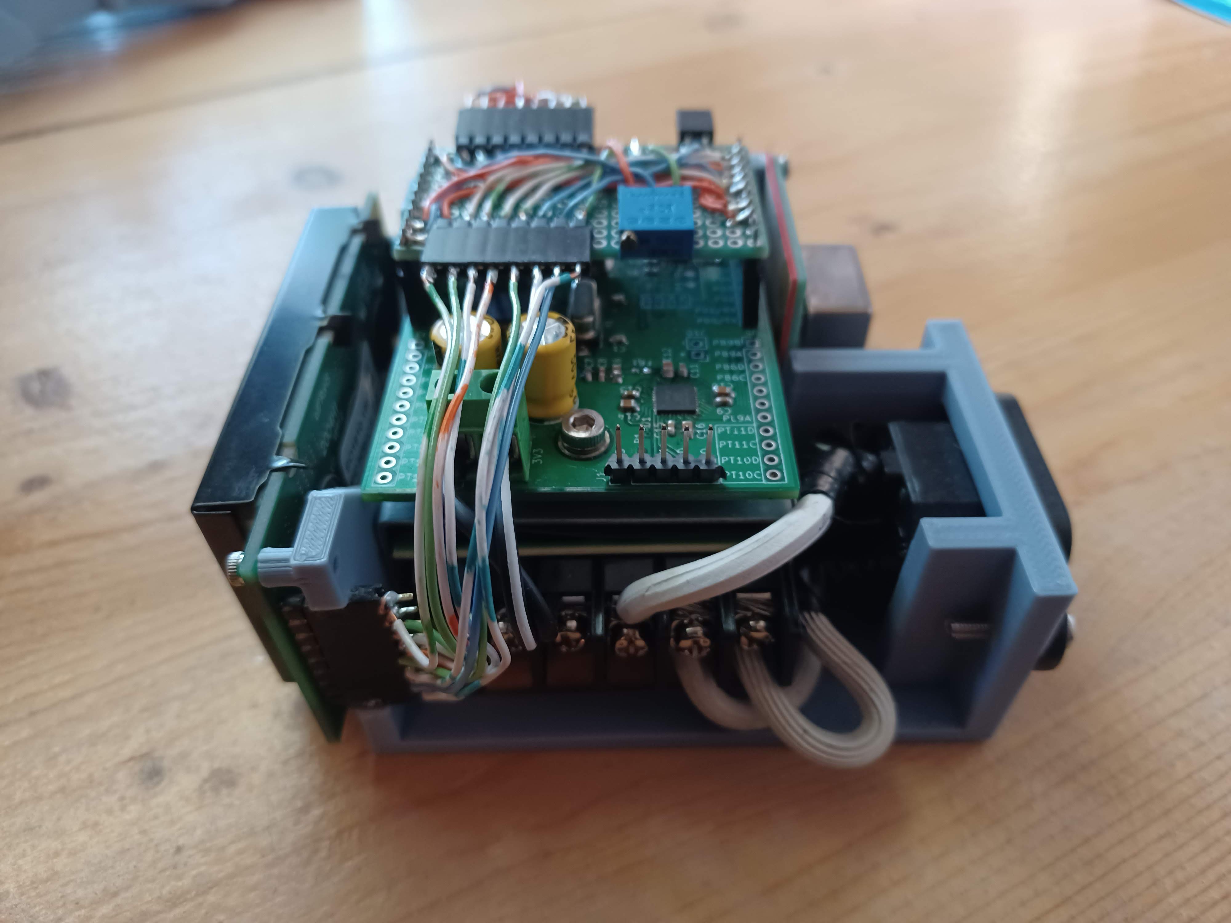
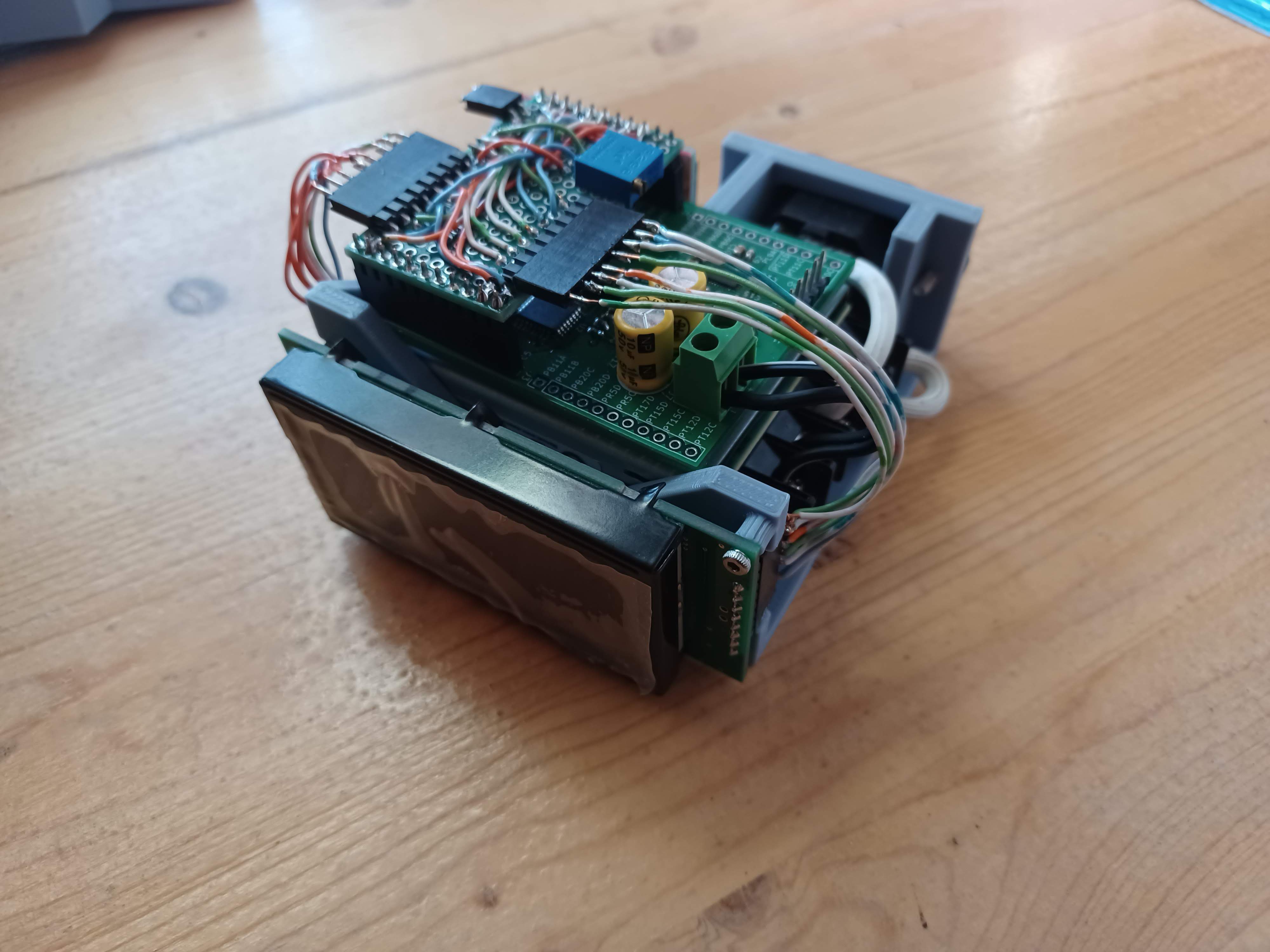
The display interface board is a little chunk of perfboard that connects wires coming from the display to the correct microcontroller pins, and sits right on top of the main board like so:
![]()
with the interconnect board installed ![]()
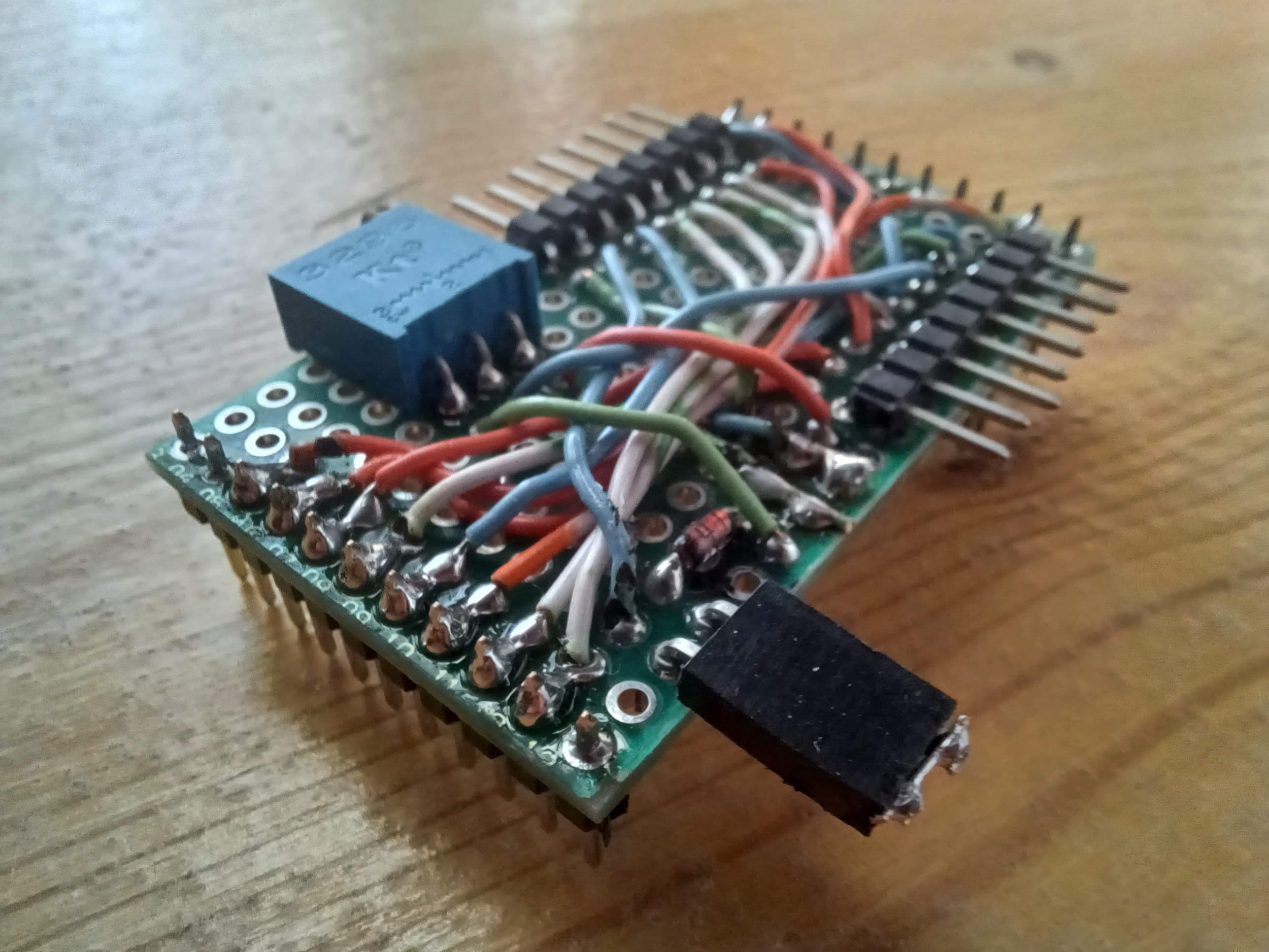
with the interconnect board out The board itself is very simple, it just has some wires, a trim pot, and a diode. The trimmer is used to set the display contrast, and the diode drops the 3v3 supply by ~0.7v for the display back light which is not rated for 3v3. Here's a pic of the interconnect board popped out of its socket:
![]()
the shorted jumper is for the back light power, so that I can have it enabled or disabled. I might eventually connect the back light to something (switch or micro pin, etc) so I left a connector.
Since I'm probably going to have to order V4 boards for this project I might also make a pcb for the interconnect board, and the master oscillator carrier board, which are both just perfboard right now. we'll see.
-
The 3D Printed Case
05/27/2021 at 20:53 • 0 commentsElectronics need to go in a box so they don't get dusty. When I started this project in 2019 I didn't have a 3D printer and so the case was built out of some aluminum duct work and scrap wood. There are pictures at the bottom of this post.
I spent most of 2020 working on my undergraduate capstone project, and due to the G L O B A L P A N D E M I C it was all done remotely. In practice this was a good excuse to buy a 3D printer since it was "for school".Now that I have a 3D printer it makes sense that I would 3D print my electronics enclosures. So that's what I'm doing.
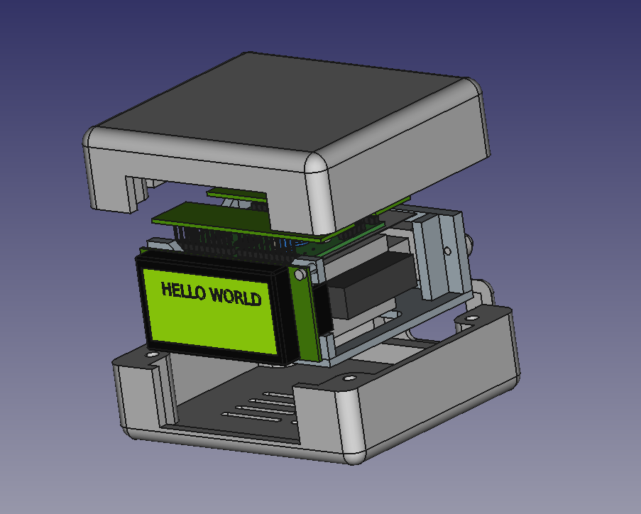
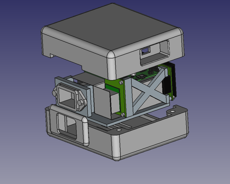
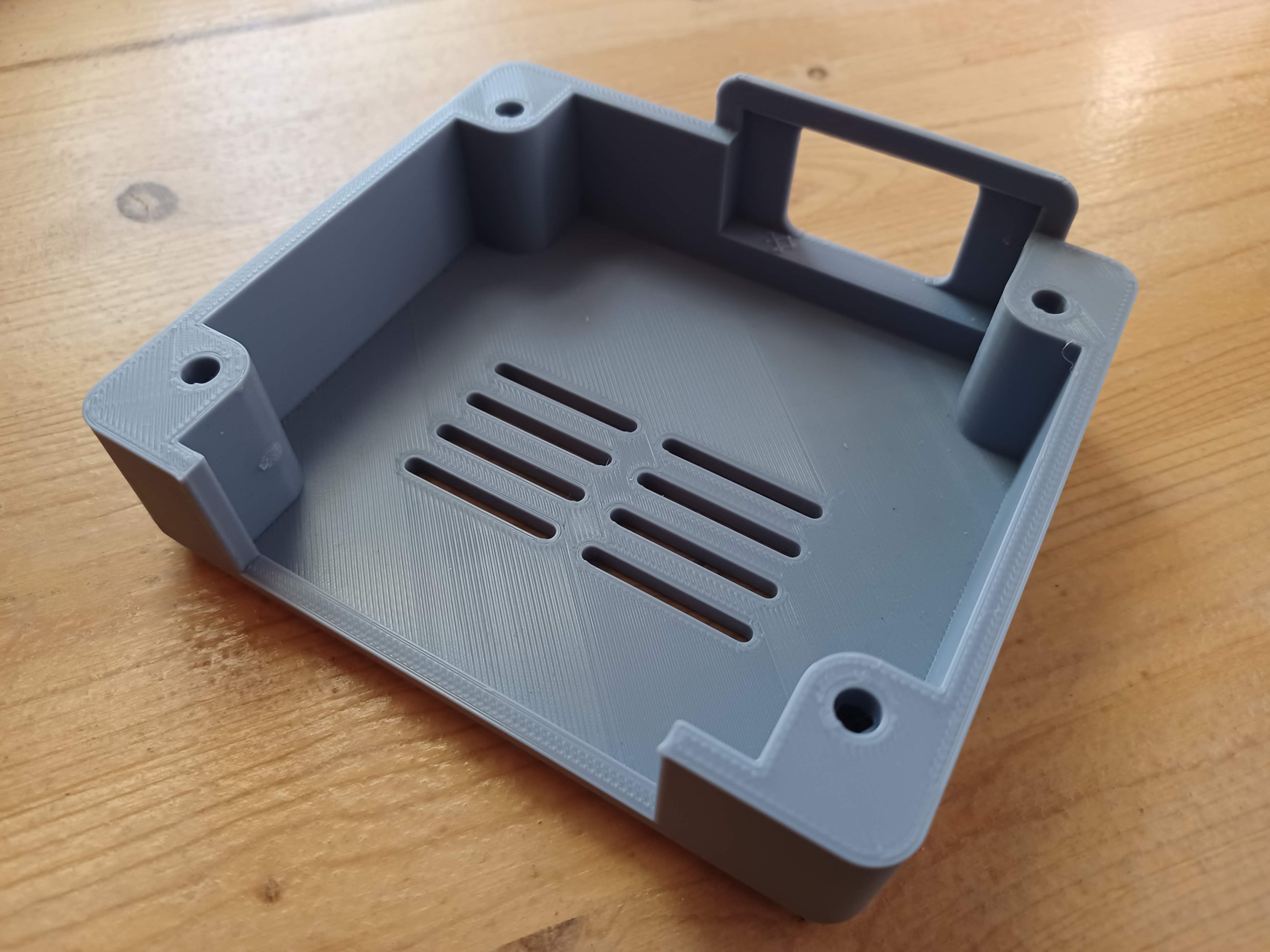
The largest component in the clock is the mains to 3v3 power supply which is a 3v3 meanwell RS-15 series unit. Datasheet [pdf]. As such I designed around the power supply. I like my projects to be easy to work on so I designed the case in 3 parts: a bottom and top cover that bolt together and sandwich a midframe assembly between them. The midframe holds all of the electronics and can be removed from the rest of the case simply by taking the top cover off. Some exploded views of the case:
![]()
![]()
There is a recess for the USB port on the left side, power input on the rear, the display on the front, and some cooling holes on the bottom. Eventually I'll also add some kind of feet as well so that the power supply gets some airflow.
The design is all done in FreeCAD, and thus far I've been printing in in PLA+ on my Ender 3. Since the top of the midframe contains a lot of interconnect wires that I didn't include in the CAD model I've held off printing the top until the project is more complete since I'm pretty sure that the top cover will require some redesigning.
In its current state the case+electronics looks like this:
![]()
The bottom cover:
![]()
and some shots of the mostly assembled midframe and electronics:
![]()
![]()