-
Rework of Sparkfun SEN-14844
03/31/2022 at 04:00 • 0 commentsTL;DR: The sensor was shorting against the groundplane of the red breakout PCB. By desoldering the sensor from the breakout board, adding some insulation to the PCB, then re-attaching the sensor, I was able to fix the intermittent fault where the thermal camera would hang during startup....
-----------------------------------------------------------------------------------------------------------------
To troubleshoot the sensor, I first downloaded a simple arduino sketch to scan the I2C bus. Search for "i2c scanner arduino" to get something similar. The scan detected my sensor every time, so I could be confident that the sensor wasn't 100% dead. However, the next step, to query the sensor for its serial number, usually failed. After reading through many threads online, I eventually emailed Sparkfun's tech support. Their reply was very quick, and helpfully pointed me to the thread at https://forum.sparkfun.com/viewtopic.php?f=147&t=55997&p=227179&hilit=90640#p227179
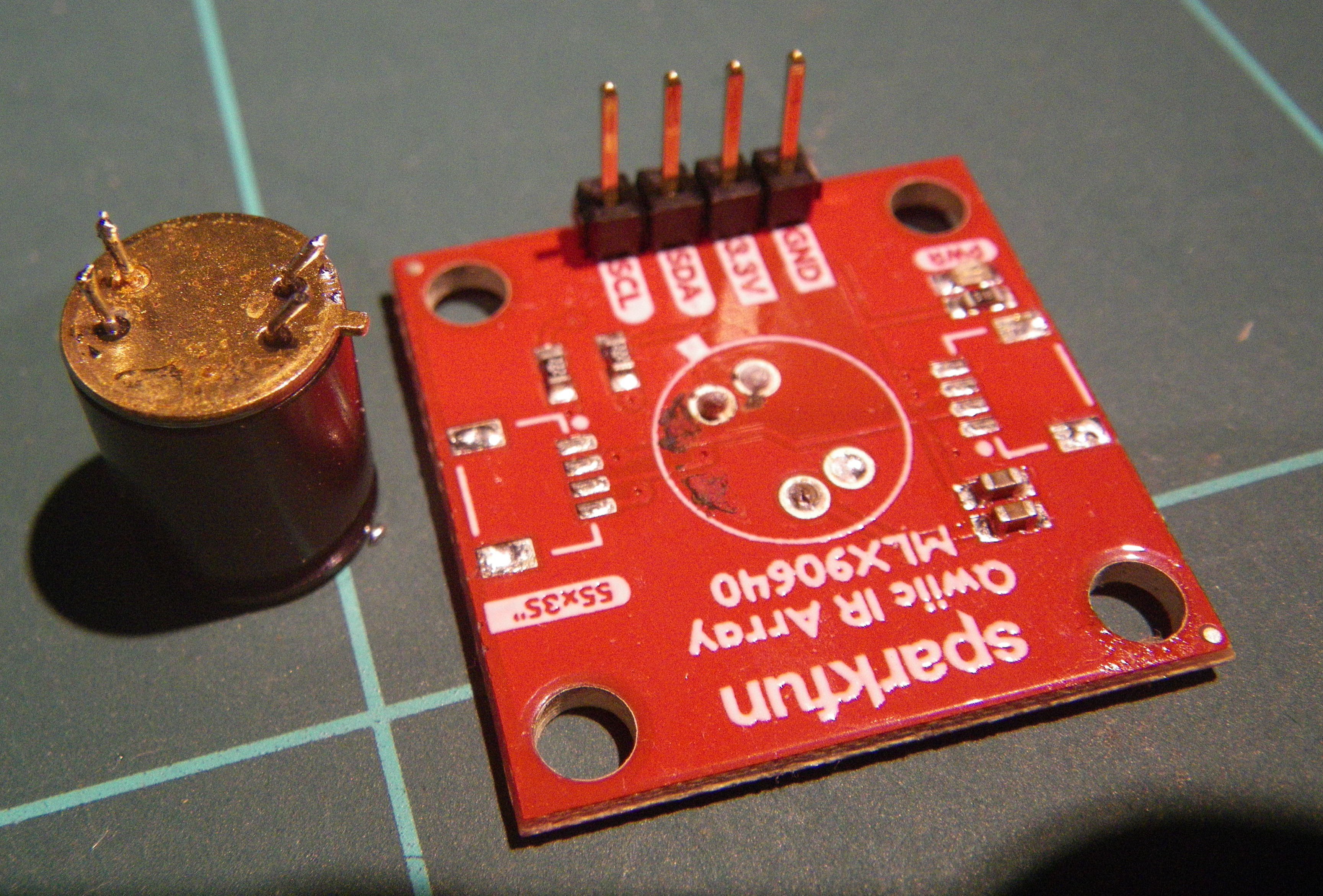
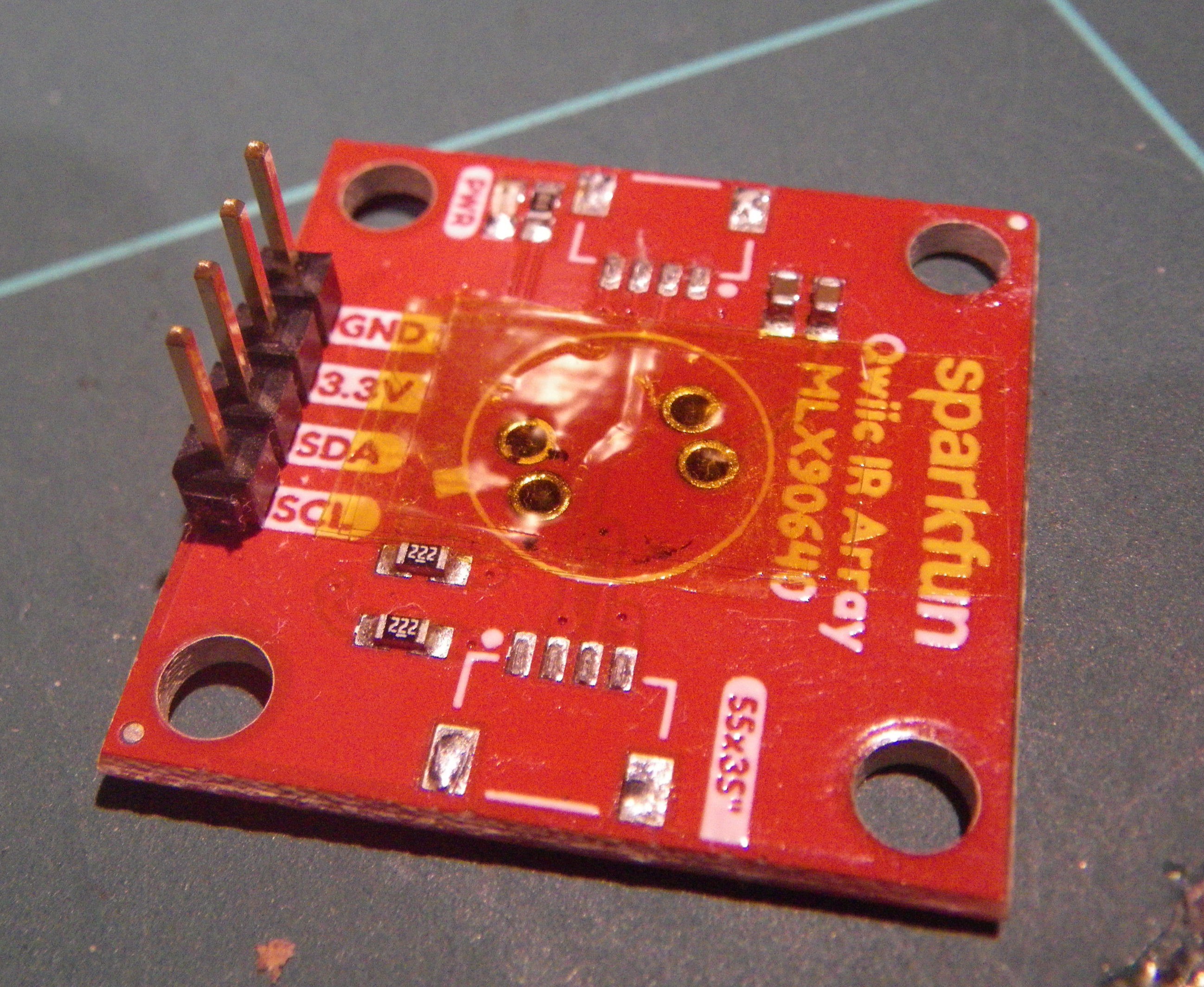
To be honest, nothing in the thread looked like the fault that I was seeing with my setup. I measured the resistances as suggested in the thread and everything checked out OK. But this is the trouble with an intermittent fault - sometimes it _looks_ OK! Being too impatient to wait for a replacement breakout board, it seemed worth a shot to to attempt the rework. I desoldered my breakout board from the thermal camera PCB. I then (carefully!) desoldered the sensor from the breakout PCB. After cleaning up the excess solder from the holes in the breakout PCB, I added a few layers of Kapton tape to insulate the breakout PCB from the sensor, then soldered the sensor back onto the PCB. I then resoldered the breakout PCB to the main PCB of the thermal camera. Success!
I was very surprised when this worked - intermittent faults are often difficult to isolate and repair, but this one was a win. I think for version 2 of my camera PCB, I will add a footprint for just the bare sensor and do away with the breakouts altogether. They are great for prototyping, but for such a simple circuit there's no advantage to using a breakout in the final product. This also aligns with my goal of trying to work around the global parts shortage - it seems foolish to design a PCB to be reliant on the third-party vendor of the breakout boards.
Having said that, I have been very impressed by the technical support from Sparkfun - thanks again!
MLX90640 sensor removed from breakout board Mounting holes cleaned up, PCB insulated with 3 layers of Kapton tape -
Issues
01/04/2022 at 08:00 • 0 commentsv0.1 has been sitting on my desk for a few months now. It mostly "just works" but recently I've been running into issues with the MLX90640 sensor not being recognised. When I get time I'll look at the I2C lines on the oscilloscope and try to work out what's going on. The Arduino software is a mess (this is why I haven't shared it yet, sorry!) but this doesn't explain the intermittent faults. More updates to follow....
-
PCB v0.1 design and errata
09/12/2021 at 04:35 • 0 commentsBefore I send a new PCB design for fabrication, it's good to double check a few items:
- Test points, for all power supply voltages, all the signals I will be using, and, if space permits, unused pins of ICs and microcontrollers, in case I want to add features later
- Silkscreen labels for all components and signals.
- this includes polarity markings for polarised components like diodes and electrolytic capacitors, and + and - signs for batteries or power supply.
- It's also a good idea to mark anything that can easily be mixed up, for example, the colours of different LEDs
- mounting holes. Even if they don't get used for mounting the PCB in the final product, they can be used to hold the PCB down during testing or assembly, and are also useful for passing wires through
- Board name and revision number. Even if I think it's a one-off.
Back when PCBs cost over $10 per square centimetre, it was important to minimise their size. Now that they are cheaper, I think improving usability of the PCB is usually a good trade off. Of course there will be exceptions!
During the present chip shortage, it's often a good idea to provide accommodation for component substitutions, if possible. This might include:
- allowing for different pin spacing on passive components like resistors and capacitors
- making room for differrent modules (like I have in this design, to accommodate the Adafruit or Sparkfun breakouts, or the bare Melexis sensor.
So, when I got the shiny v0.1 PCBs from the factory, I noticed that I had made one mistake and somehow swapped the SCK and MOSI lines for the screen on the schematic! Stupid. I had to mend this on the v0.1 PCB by manually soldering wires at R6 and R7. After a bit of testing, I also noticed that the readout for battery voltage is quite noisy. My oscilloscope shows ~230mV of ripple at ~150Hz on the input side of the DC-DC converter. The noise seems similar regardless of whether the unit is running from batteries or a lab power supply. Regardless of the cause, a capacitor between the ADC pin and ground helps smooth out some of this noise. To fix the v0.1 board I added a 1µF SMD capacitor (the first value I had at hand) in parallel with R9. Before I added the capacitor, ADC readings would fluctuate by ~50, the capacitor reduced them to ~3. It’s probably better to use a couple of caps of different values to remove different frequencies of ripple, but the 1µF is definitely "good enough."
There may be other mistakes that become apparent as I do more testing. There will definitely be features I want to add, and the community might have suggestions too! at some point I would like to do a second revision of the PCB, but at this stage I don't have enough information to commit to a v0.2. The v0.1 is more than sufficient for testing.
-
Testing
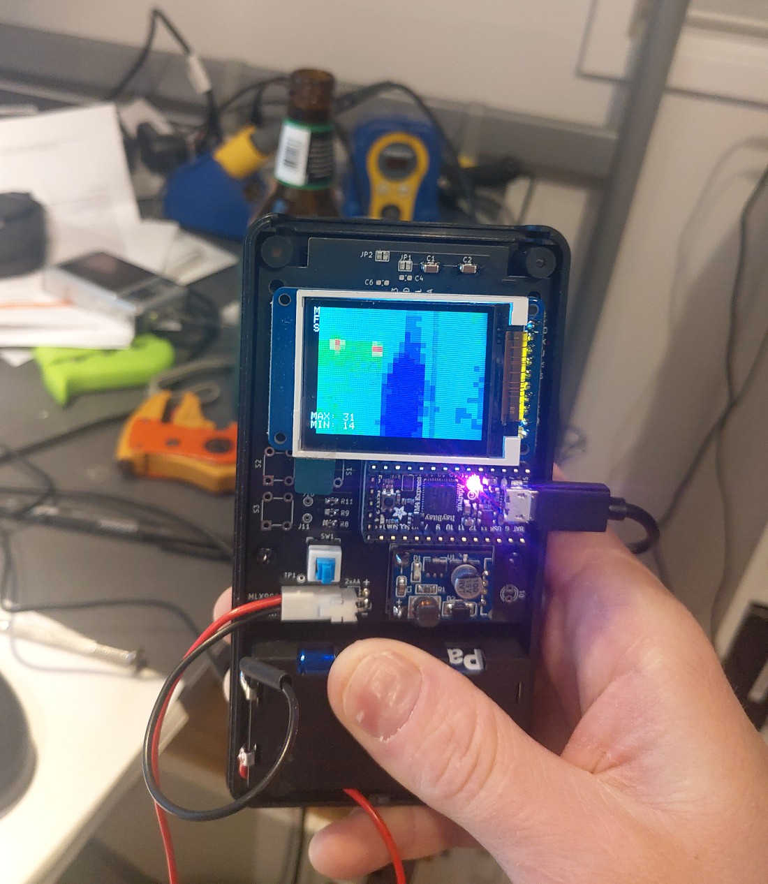
08/22/2021 at 07:46 • 0 commentsIt works!
The bottle of beer on my desk shows up colder than the background, and there are two power adapters that appear as warm spots behind that. There are a couple more pictures of the camera in action in the Gallery.
![]()
-
More assembly notes
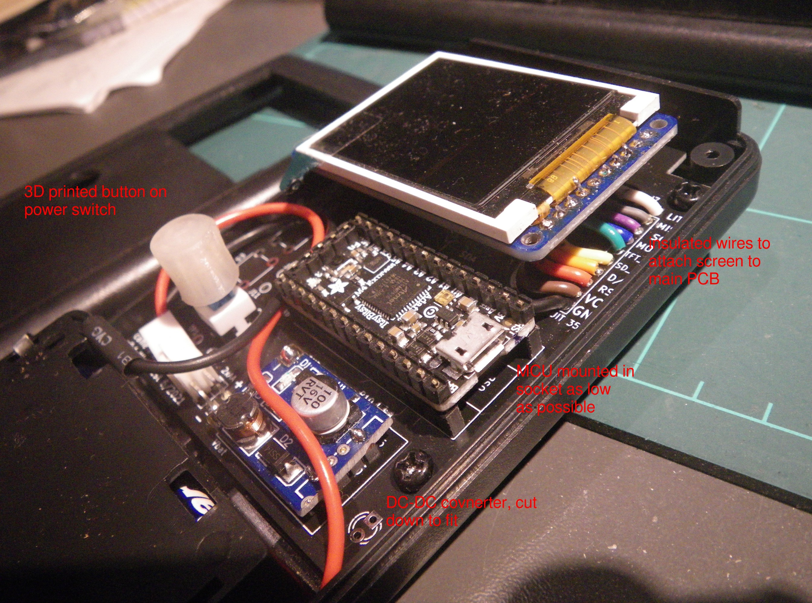
08/22/2021 at 07:20 • 0 commentsI had hoped that I could use header pins on the screen to sit in a socket on the carrier board. This would have allowed me to detach the screen easily if i needed to make modifications, measurements or repairs to the thermal camera.
The detachable screen worked well enough for testing, but would often go blank if it received a slight push in the wrong direction.
So I desoldered the socket and header pins, and replaced them with short lengths of insulated hookup wire. Now the screen is much more reliable! There is enough "flex" in the wires that it is easier to fit the screen into its matching cutout in the case. You can't see it in the pictures, but there's a piece of foam behind the screen to keep it level with the main PCB and gently push it into the cutout in the lid of the case, so that everything is held snugly without rattling.
The switch was the smallest "latching" switch I could find in stock at Digikey. I 3D printed a round button for the switch, because is it easier to make a round hole in the case than a square one :-)
You can also see in the photo that the MCU needs to be mounted as low as possible in its socket, so that the lid of the case will still fit.
![]()
-
Assembly notes
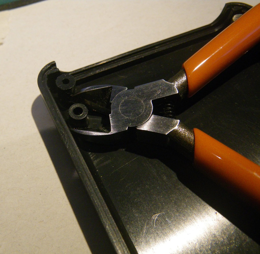
08/21/2021 at 08:55 • 0 comments- Two unused mounting points in the "top" of the case need to be removed to provide clearance for the screen.
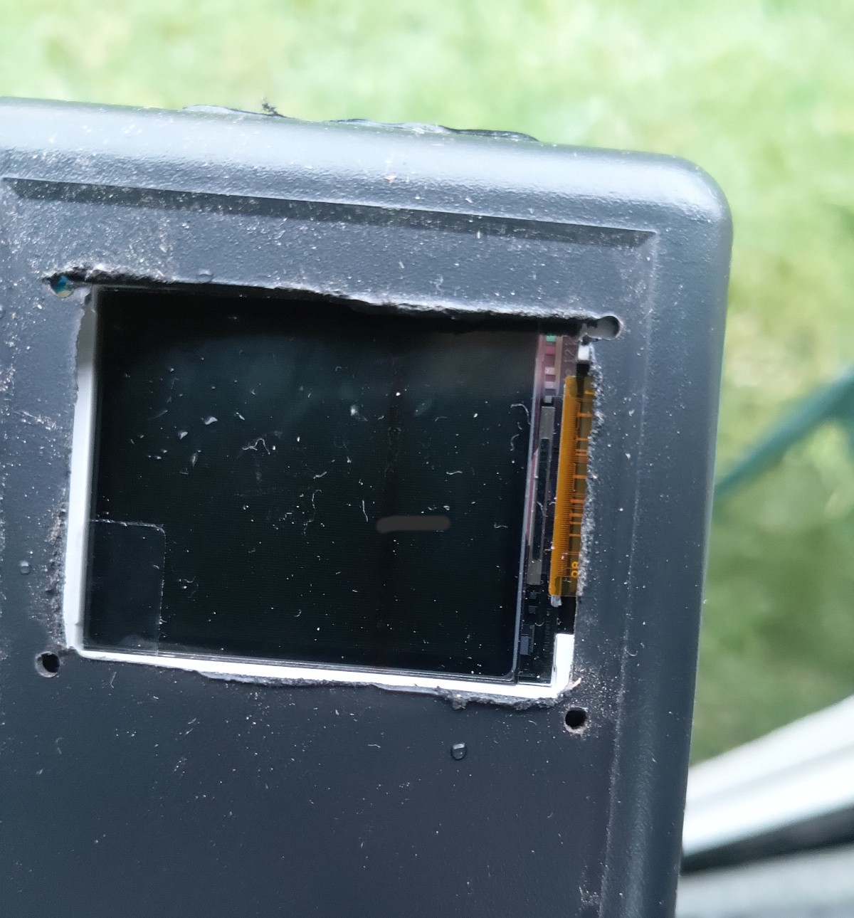
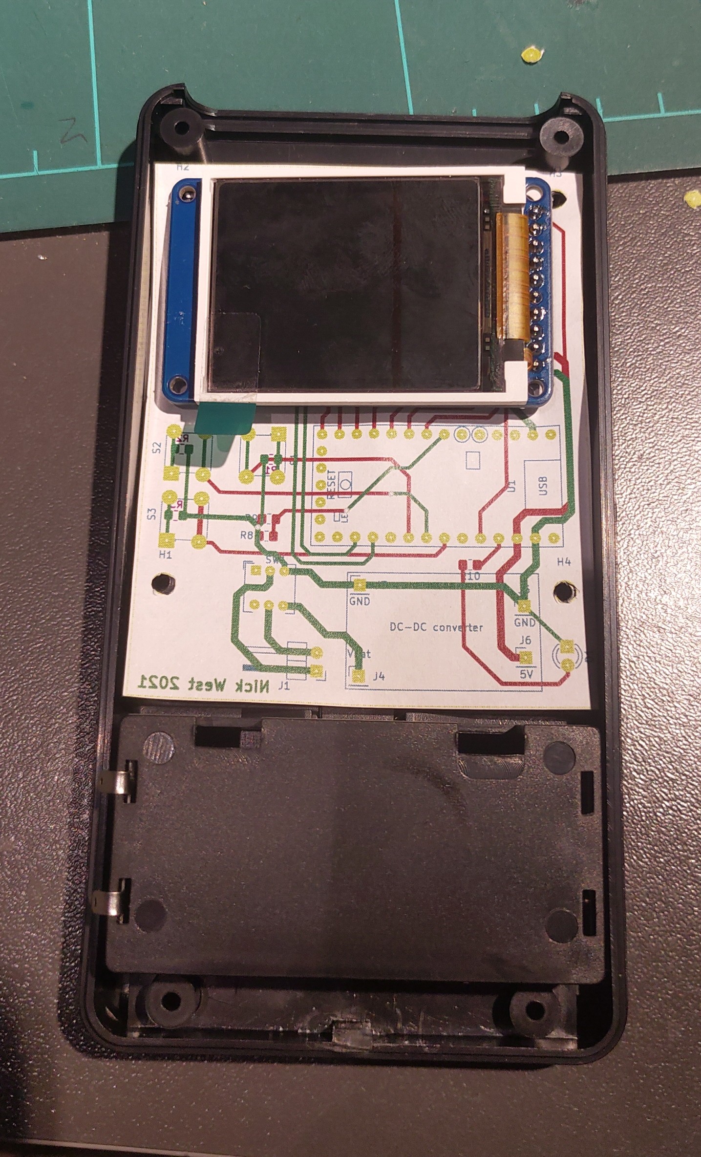
- The top of the case also needs holes for the switches, and a big rectangular cutout for the screen. Start with smaller holes than you think you need, then check for alignment. You can also use the PCB as a guide, or a copy of the PCB printed on paper. If you use a paper printout, you can drill right through it if necessary.
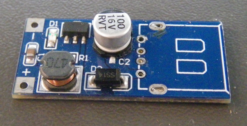
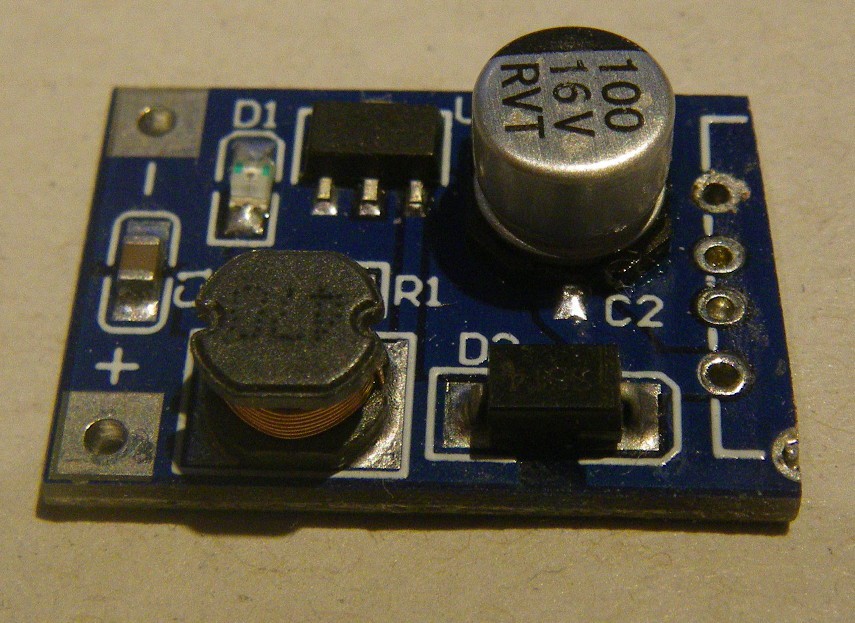
- Depending on the DC-DC module, you may need to modify it to fit. I had to remove the big USB socket and then cut down the module's PCB. A hacksaw with very fine teeth works, or you can deeply score the PCB with a knife and then bend it until it snaps along the cut.
![]()
-
Sanity check the PCB
08/21/2021 at 08:16 • 0 commentsBefore I sent the PCBs files away to be fabricated, I like to print them on paper to look for mistakes and to check the PCB will actually fit where it's supposed to. You can also poke holes in the printout to check for alignment of mounting holes and that connectors etc will fit OK.
It's not foolproof but it costs virtually nothing to do.![]()
-
Enclosure Assembly
08/18/2021 at 05:43 • 0 commentsMaking the case pretty would be much easier if you have a laser cutter or a CNC mill. I have neither! I've tried to minimise the number of straight cuts and square holes required, by using round buttons wherever possible.
I suppose you could also 3D print a case, to avoid any cutting at all. If there is demand, maybe I will design one! For now though, the Serpac “HP65” series of enclosures seem quite easy to find, cheap to buy, and reasonably straightforward to modify.
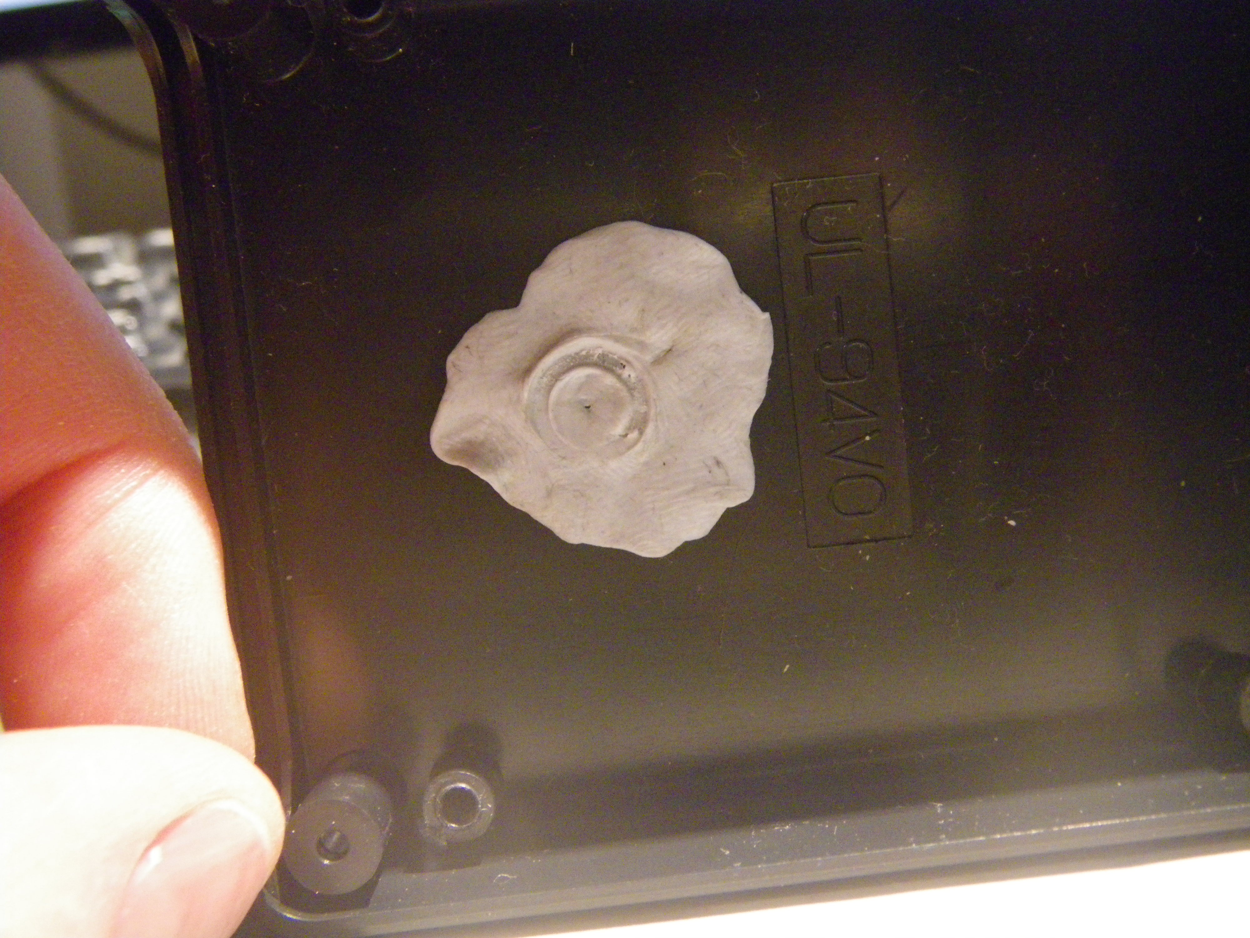
One thing that gave me trouble was getting a well-placed hole for the lens to poke out the "back" of the camera. I achieved this after attaching the Sparkfun MLX90640 breakout to the main PCB carrier board. Then I put a ilttle bit of Blu-Tac on the case where I thought the lens would go. I smeared the Blu-Tac out so it was flat and covered a few square centimetres. Then I carefully laid the carrier board over the case, so the lens left an impression in the soft Blu Tac. this gave me a location for a pilot hole. When the pilot hole was drilled, I could remove the Blu-Tac and enlarge the hole to suit my lens. If your hole looks a bit messy, I've made 3D printable bezel to hide the cutout.
Simple Thermal Camera
A thermal camera using a 32 * 24 pixel sensor. Designed to allow lots of substitutions due to the parts shortage!
