Close
0%
0%

Linux Capable Business Card

ARM926EJ-S 400MHz CPU with DDR2-533 RAM Running Linux

Similar projects worth following
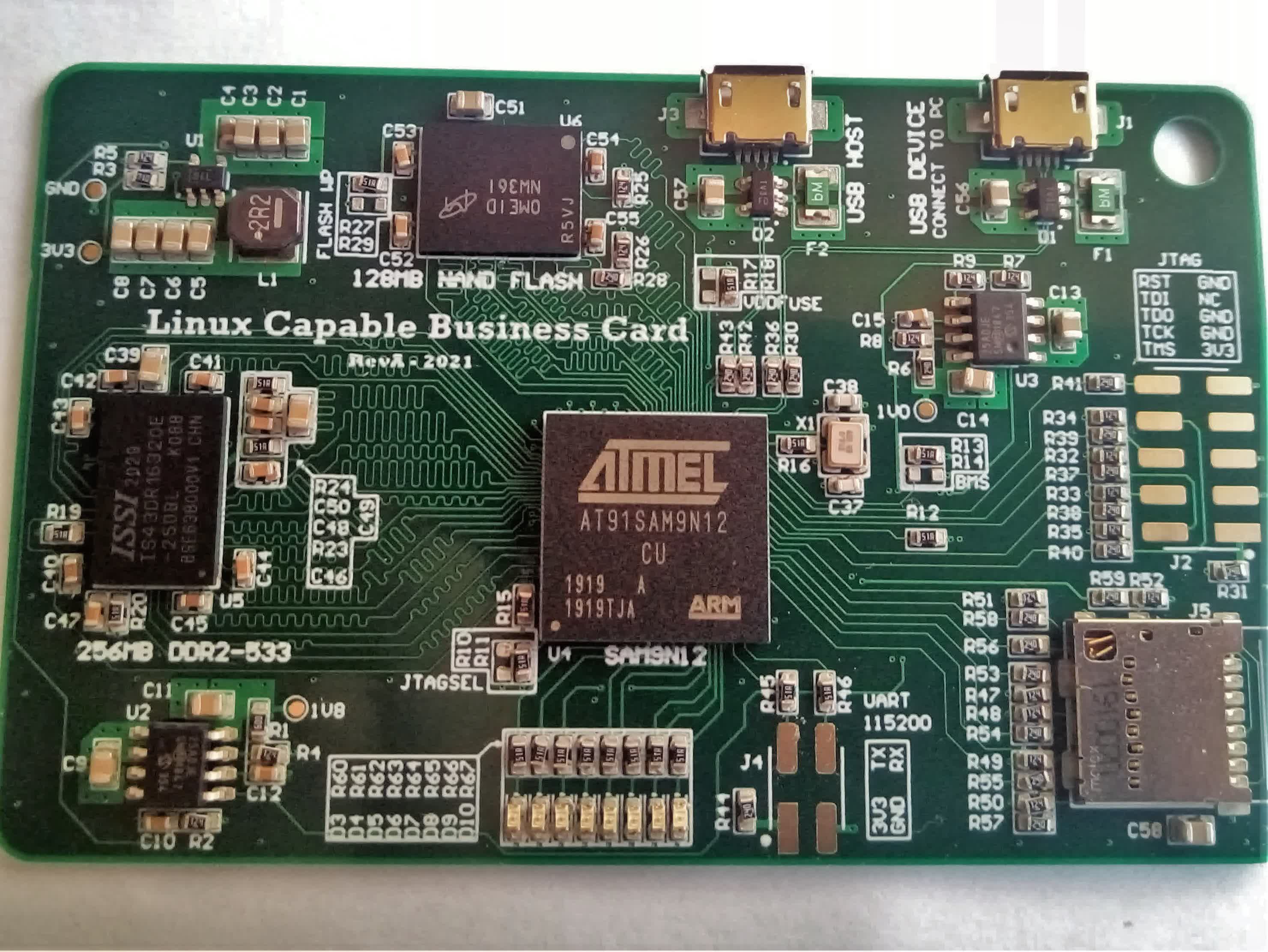
- Microchip AT91SAM9N12 microprocessor, ARM926 core running at 400MHz
- 256MB RAM DDR2-533
- 128MB of NAND FLASH
- micro SD-Card slot
- 8x LEDs

PCB design, assembling, and testing.

Block Diagram

I wanted to design a more complex board, something with DDR memory and a CPU that can run Linux. This board includes a 400MHz ARM processor with DDR2 RAM and NAND FLASH. I don't care about the usefulness of this board, it only serves as practice with high-speed design.

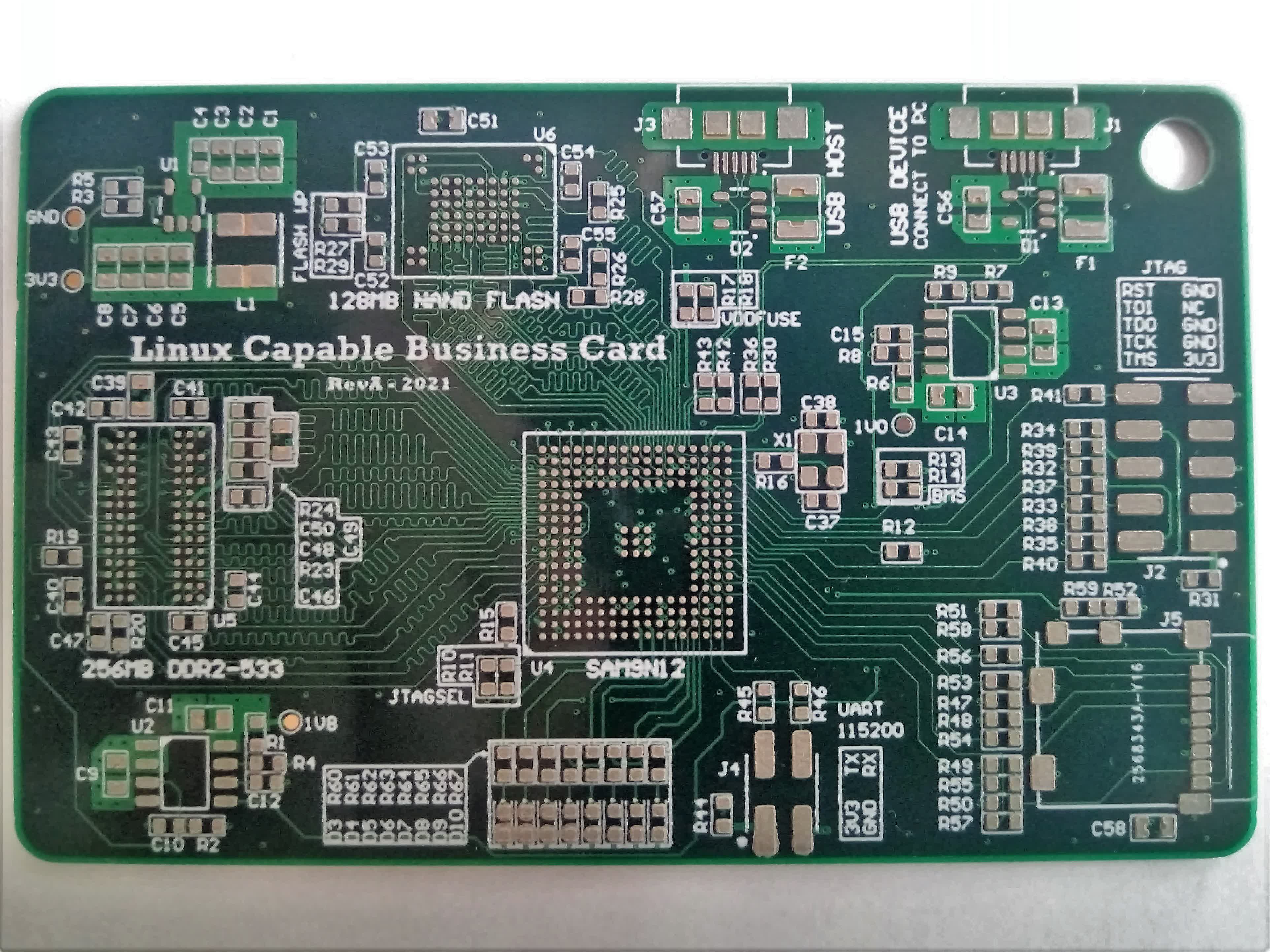
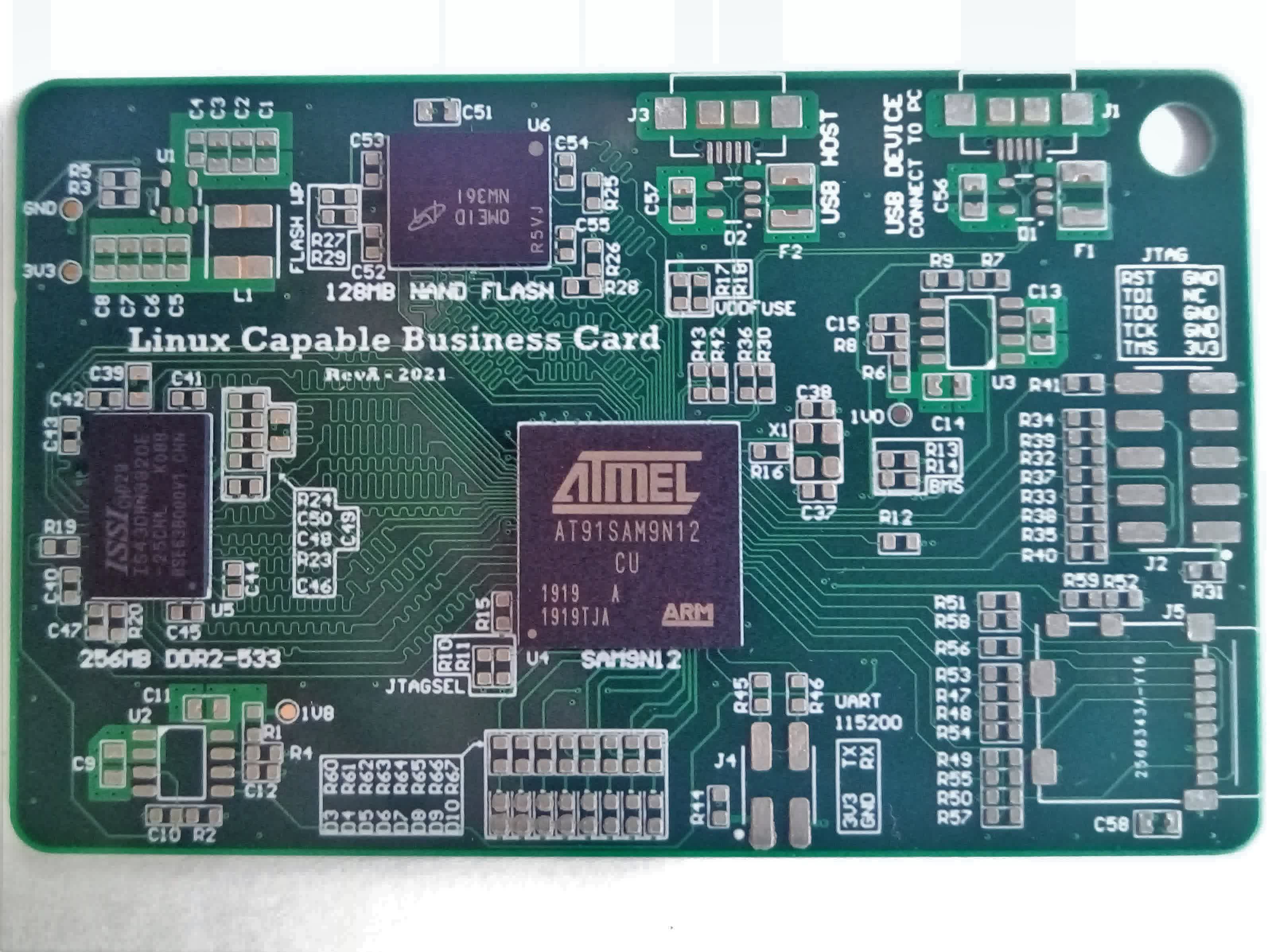
The circuit is very simple, it is built around the AT91SAM9N12 MPU. The board supports up to 256MB of DDR2 RAM and 128MB NAND FLASH. There are two USB ports one HOST and one DEVICE. The DEVICE port is used to load the firmware and connect to a Linux terminal through a virtual com port. The HOST port can be used to connect external peripherals to the board (wifi dongle for example). For debugging there are UART and JTAG connections. The micro SD card can be used as external storage or as a boot device.

The power supply is a little more complicated. The USB 5V is lowered to 3.3V with a buck converter. The 3.3V is then lowered to 1.8V and 1V with linear LDO regulators. To ensure relatable operation the power rails need to come up in a specific order. The enable and power-good signals from the regulators are used to generate the proper sequence (first 3.3V, then 1.8V, last 1V) and to keep the CPU in reset until the power is stable.

The schematic document can be found here.
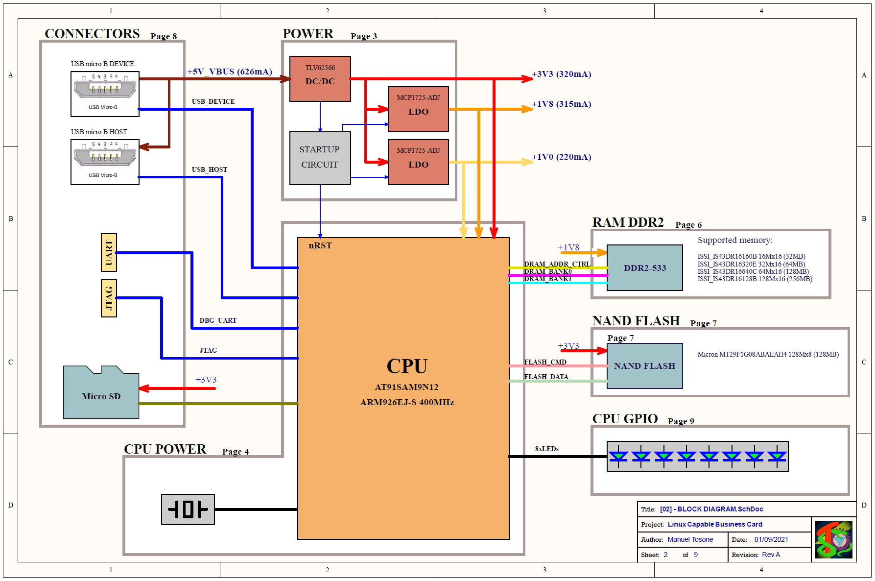
Block Diagram

PCB Considerations

To keep the cost down I want to make a 4 layer board. To manufacture the boards I'll use the JLCPCB service since it is the cheapest that I know of that can manufacture 3.5mil (0.09mm) minimum track width and spacing. To route the DDR interface properly, all the tracks from the two data banks must be routed on the same layer with a solid ground plane underneath. To achieve that on a 4 layer board it is necessary to route two tracks in between BGA pads. BGA packages on this board have a 0.8 mm pin pitch. Making the pads 0.35mm in diameter leaves just enough space for two tracks with the minimum width and spacing.

Stackup

For controlled impedance stackups there are two options, they differ in the prepreg and core thickness. For this project, I'll go with the second option (JLC2313 Stackup). Having the reference planes closer to the signal layers reduces crosstalk and, for a given impedance, the traces are smaller.

The 4 layers are utilized in the following manner:

  • Layer 1: Almost all signals, RAM data banks are routed only on the top layer with a solid ground plane directly below, on layer 2.
  • Layer 2: Solid ground plane.
  • Layer 3: Power plane. The 1.8V power plane is the reference for the RAM address command and control signals.
  • Layer 4: RAM address command and control signals referencing the power plane above. Ground pour to balance construction.
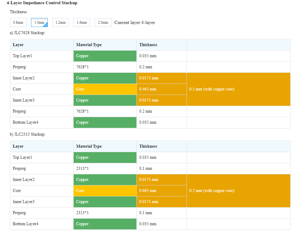
Stackup

For signal integrity, it is required to control the impedance on high-speed interfaces. In other words, the tracks must be made a specific width that's based upon the stackup. For differential pairs, the distance between traces also depends on the stackup. 

The impedances are as follows:

  • Most of the tracks are routed as 55 Ohm, including DDR2 data and address signals.
  • DDR2 clock differential pair 100 Ohm differential.
  • USB differential pair 90 Ohm differential.

Using the JLCPCB impedance calculator, the required trace width and spacing have been calculated.

LayerImpedancetrace widthspace
TOP/BOTTOM55 Ohm SE4.73 mil (0.120 mm)-
TOP/BOTTOM90 Ohm DIFF5.55 mil (0.141 mm)6 mil (0.152 mm)
TOP/BOTTOM100 Ohm DIFF4.35 mil (0.110 mm)6 mil (0.152 mm)

PCB Layout

I made a 15-minute video where I go through the layout of the board. The actual layout took roughly 20 hours.


  • Booting Linux from SD Card

    Manuel Tosone09/17/2021 at 09:57 0 comments

    Assembling

    The board is hand-assembled. I use a stencil to spread the solder paste and then the components are placed with tweezers. When working with BGA packages I always place them first. To check the alignment, I look under the package from its side, If I can see light in between every row the component is aligned. Using a thicker paste it is possible to tweak the position of the package by bumping it from the side without smearing the paste. When the component is in place I lightly push down on it to make sure every ball is in contact with the paste. At this stage, If I screw up the placement, I can always clean the board and start over with minimal drama. When all the BGAs are in place, I position the other components starting with the hardest. Soldering is done with hot air. Managing the heat is a little tricky, mostly because it's hard to tell when the BGAs are soldered properly. What works for me, is to set the temperature to 100 °C and preheat the entire board for about two minutes, then I increase the temperature and start reflowing component by component.

    First Power Up

    Applying power for the first time is always a little scary.
    First, with a multimeter, I checked every power rail for shorts. Next, I connected the board to a current limited power supply and measured the voltages on the tree test points. The voltages were good. There is a sequence in which the power rails must come up to ensure proper operation. The correct order is 3v3, 1V8, 1V0, with the CPU reset releasing last. Looking at the scope capture below we see that it is correct.

    The last check is to see if the oscillator is running, and it is. That's promising, we might have a working board!

    Linux kernel and Buildroot

    I'm no expert when it comes to embedded Linux. Since this is my first time using buildroot to compile Linux from scratch, I won't try to explain how it works (I barely understand it myself ;) ) but I will link to some good resources in case you want to learn more.

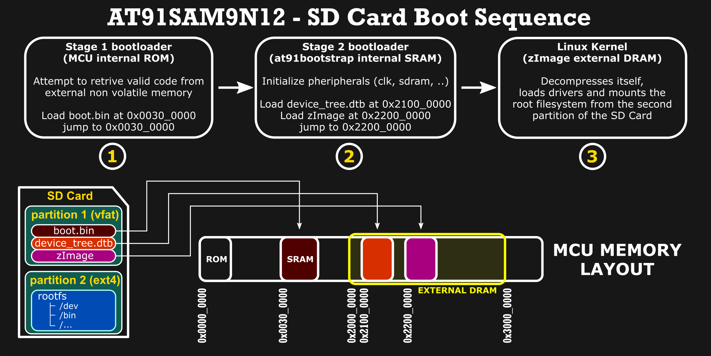
    To keep things simple I've decided to have the second stage bootloader loading Linux directly instead of using a third stage like u-boot.

    The boot process starts with the first stage bootloader that resides in the internal ROM. It tries to load valid code from external non-volatile memories. When booting from the SD Card it looks for a “boot.bin” file (second stage bootloader) in the root directory of a FAT12/16/32 partition. That file is copied to the internal SRAM and executed.

    The second stage bootloader initializes the hardware, loads the device tree and kernel image to the external DRAM. After that jumps to the kernel image that is self-extracting (it decompresses itself inside the memory). Then the kernel loads the root file system from the second partition of the SD Card.

    RAM Troubleshooting

    After putting the image on the SD Card and connecting to the debug serial port, I applied power through the USB. The board Initially seemed to work fine, the SD card was detected, the second stage bootloader was able to run and load the kernel. It was all fine until the MPU started executing code from the external DRAM, there was some text output from the kernel but then it just kernel panic and gave up trying. On subsequent attempts it didn't behave consistently, the system did freeze or kernel panic at different times. After enough tries, it managed to boot and I was able to log in, from the terminal I tried to run memtester (userspace tester for stress-testing the...

    Read more »

View project log

Enjoy this project?

Share

Discussions

Zumvu wrote 09/30/2024 at 10:37 point

I recently got my hands on a Linux-capable business card, and it's a game-changer! The convenience of having a mini-computer with me all the time is fantastic. It’s perfect for quick tasks on the go. Speaking of efficiency, if you’re looking to streamline your scheduling, check out the https://blog.zumvu.com/calendly-alternatives They can really help optimize your time management!

  Are you sure? yes | no

Clara Bartoletti wrote 08/01/2022 at 13:37 point

This is a typical business card that I have designed and created. It has the logo of my company, name and contact details. I believe this is a great way to advertise your business because it can be seen by anyone who wants to visit your website or social media profiles. Being a tech person, I love exploring calendly-alternatives.org and other such platforms for providing the best experience to my customers. I am a Linux user and I have been using this card for a long time.

  Are you sure? yes | no

iAmInAction wrote 10/22/2021 at 14:20 point

But can it run doom using libcaca?

  Are you sure? yes | no

Similar Projects

Does this project spark your interest?

Become a member to follow this project and never miss any updates