Prologue
CIAA is the Spanish acronym of "Argentine Industrial Open Computer". It is a collective, open hardware project run by several universities across the country. The goal is to develop and promote cost-effective, industrial embedded systems to fulfil the needs of small and medium-sized enterprises.
The original CIAA hardware integrates an NXP LPC4337 dual-core microcontroller with external SDRAM, Flash memories and standard industrial control hardware peripherals: ethernet, RS-485, Opto-isolated inputs, and relay and FET outputs. A development kit called "Edu-CIAA" targets educational environments. It uses the same microcontroller but has no external SDRAM, Flash or specific input/output capabilities. It is a simple, inexpensive single-chip board with LEDs, pushbuttons, a UART and an integrated JTAG debugger based on FTDI FT-2232.
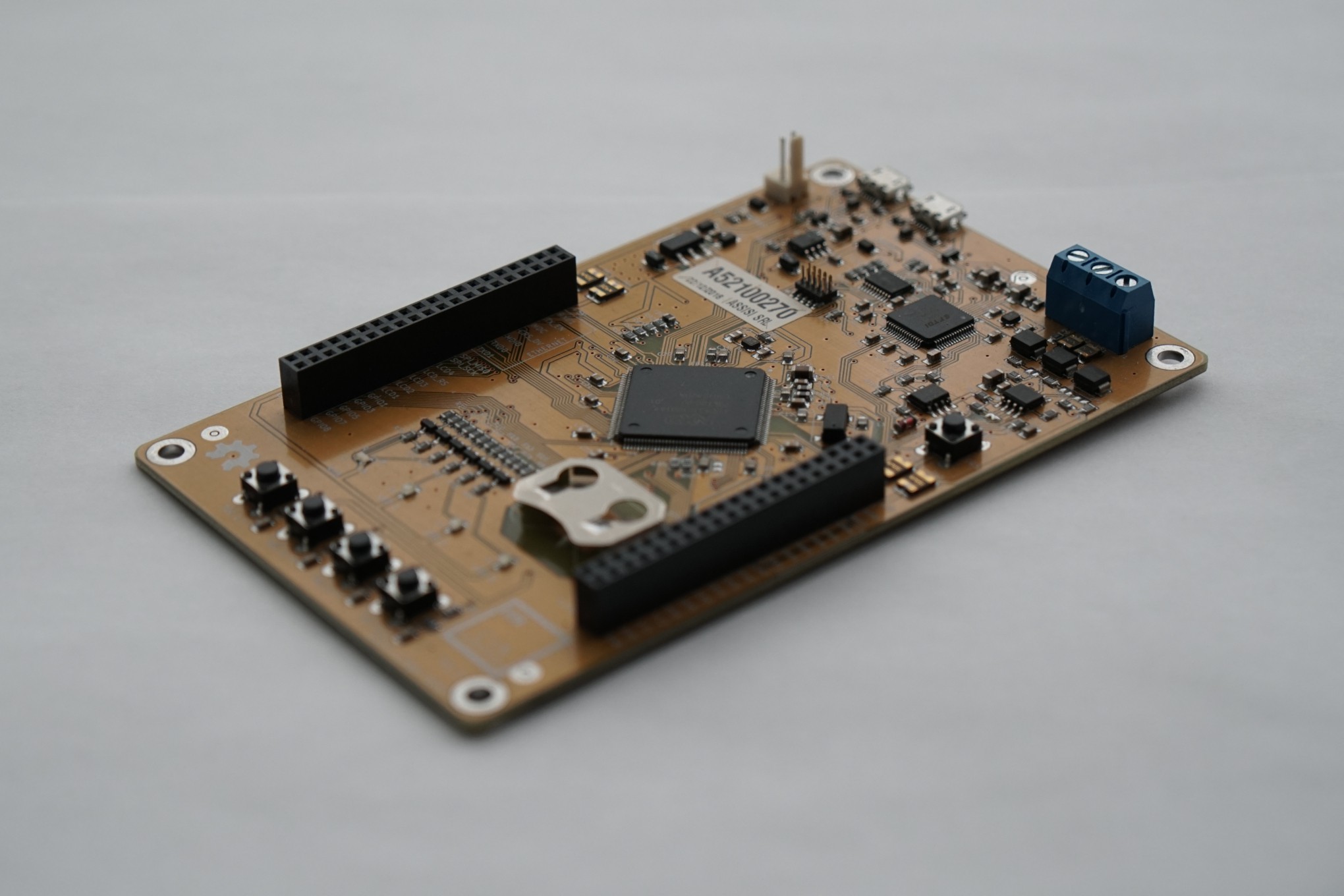
Several local embedded system courses and workshops uses Edu-CIAA as its target hardware. I had a first hands-on approach to this kit when I was taking a Master in Embedded Systems class at the University of Buenos Aires, and I was puzzled by the fact that the second core was unused. I thought it'd be great to work with graphical user interfaces since the entire embedded industry moves in that direction. And it would be awesome to have that capability almost for free by squeezing every bit of power from the same available platform we were already using.
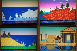
I named that project "RETRO-CIAA" for the resulting graphical retro aesthetics and because an old-fashioned game console concept should be appealing to other students. I have carried it out as final first-year work on said Master, and it is updated and extended ever since.
Development kit microcontroller details
The NXP LPC4337 is a 204 Mhz, dual-core ARM Cortex-M microcontroller. Instead of symmetric cores commonly found on PC hardware, it integrates asymmetric ones: an ARM Cortex-M4F core and an ARM Cortex-M0 core as a coprocessor of the former. The M4F implements a single-precision floating-point unit, some specialized DSP instructions and generally executes processor-intensive tasks; it is where the main application runs. The M0 core is usually employed to assist the M4F in performing asynchronous, concurrent input/output handling without delaying the main application.
136 Kb of internal SRAM and 1 Mb of internal Flash are available, shared by both cores. The entire memory map, including MCU peripherals like the UART, can be concurrently accessed, requiring software arbitration to assure coherent, ordered resource access and usage. NXP provides a generic mechanism for inter-process communication by message passing that is not suitable for this application.
SRAM and Flash divide into various segments of non-contiguous memory areas. There are two 512 Kb Flash banks, Bank-A and Bank-B, and several SRAM banks connected to different microcontroller internal busses. In turn, each core resides on one of those buses. So although nothing is preventing both from accessing all resources since buses are bridged, all accesses do not perform equally fast. Most resources are optimized for (in fact, the official documentation enforces) a given usage pattern that, to make this happen, I will need not follow :)
Project implementation overview
A video adapter is a device that converts an image -or frame- represented in video memory to a signal that a monitor can decode and display. A video mode represents a given frame rate (images per second) and resolution (width and height) measured in pixels. The frame buffer is an area of video memory dedicated to storing the pixels of a single frame. A pixel is a unit of information that contains the colour it depicts, either indirectly by being the table index where the colour information is stored or directly by specifying the additive amounts of red, green and blue components as bits inside the same pixel. A pixel is positioned on the frame buffer memory by its X and Y screen...
Read more » Santiago Germino
 Keith
Keith
 Sundance Multiprocessor
 Martin Piper
 Nicola Wrachien