-
Version 5
09/17/2021 at 07:26 • 0 commentsVersion 5
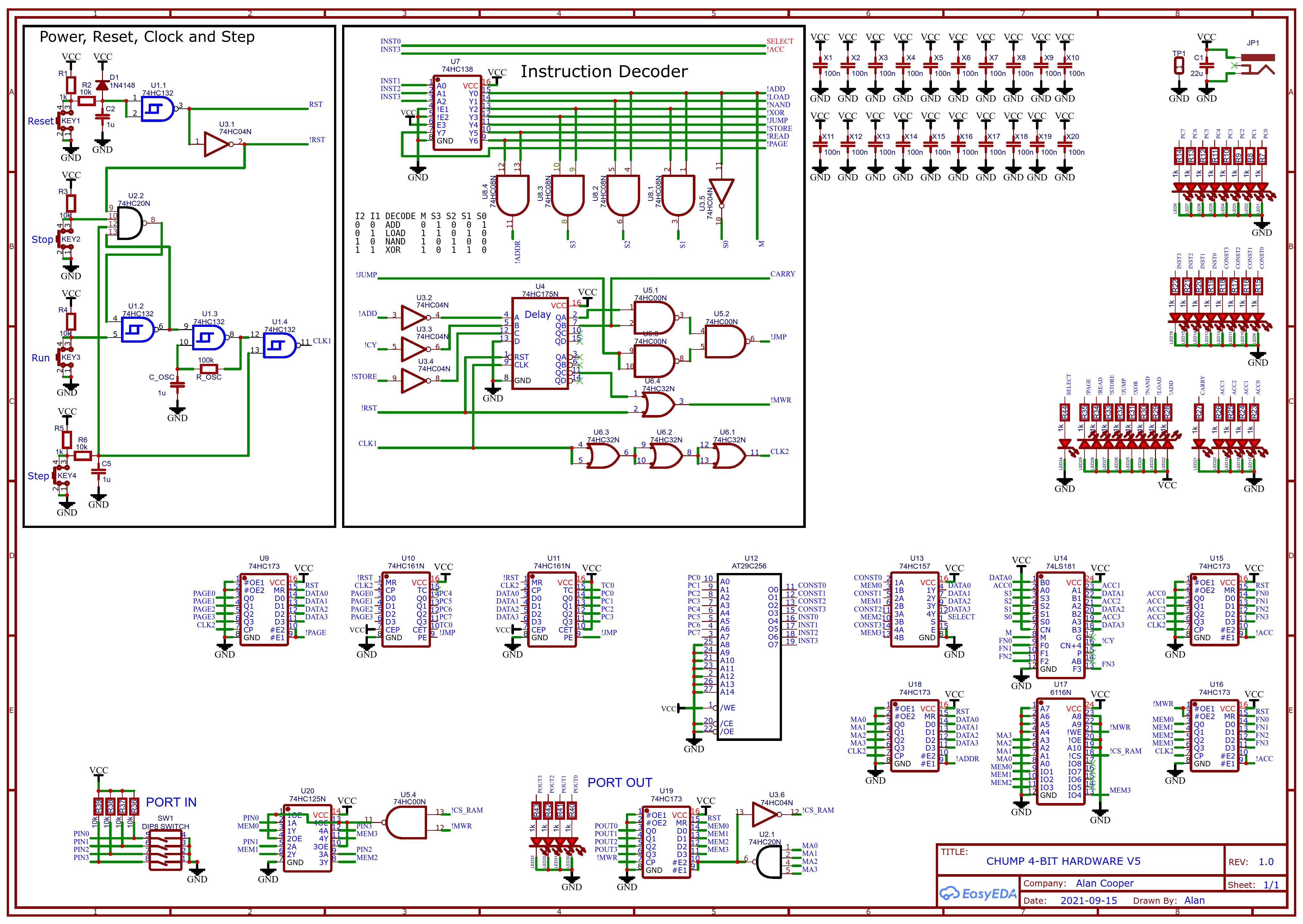
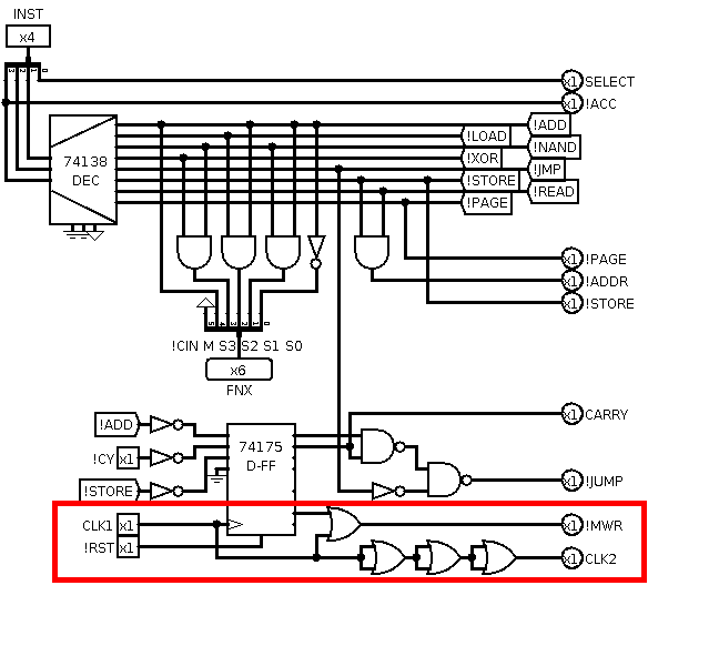
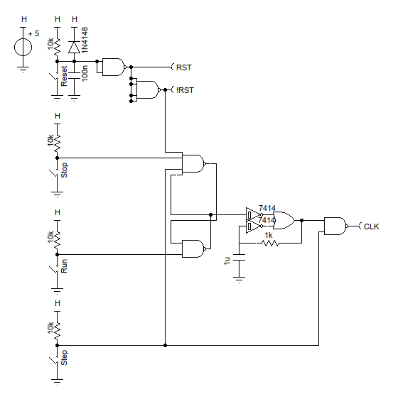
Version 4 did not last long! I have opted to use memory mapped Input/Output (IO) and an upgraded Reset/Clock/Step logic:
![]()
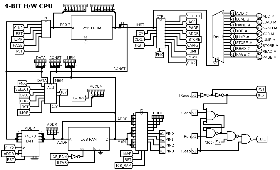
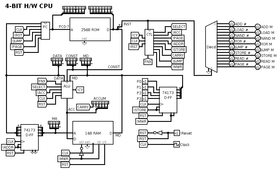
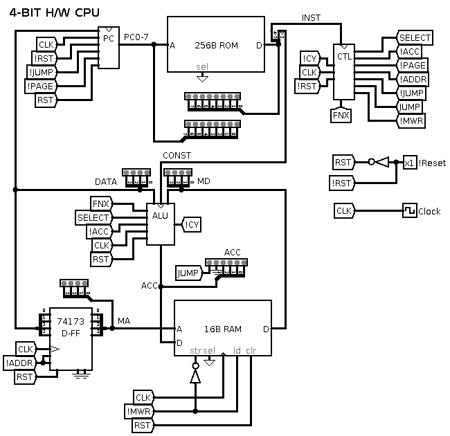
I have updated the LogiSim model as well:
![]()
OpCode Improvements
Addressing the memory timing issues had the side effect of resolving post STORE issues. Now two STOREs can be sequential and reading memory after a STORE will return the stored value (which is the same as the ACCumulator value).
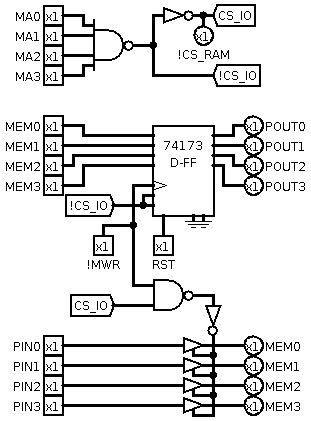
Input/Output Design
Here is the LogiSim IO design:
![]()
Note: Memory Address 0xF is now used for IO.
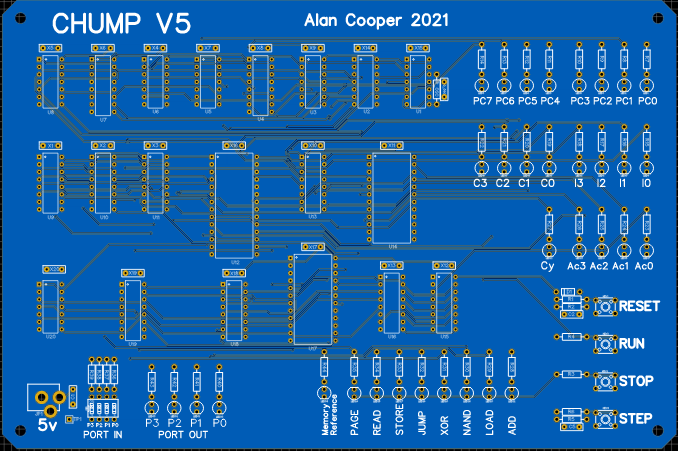
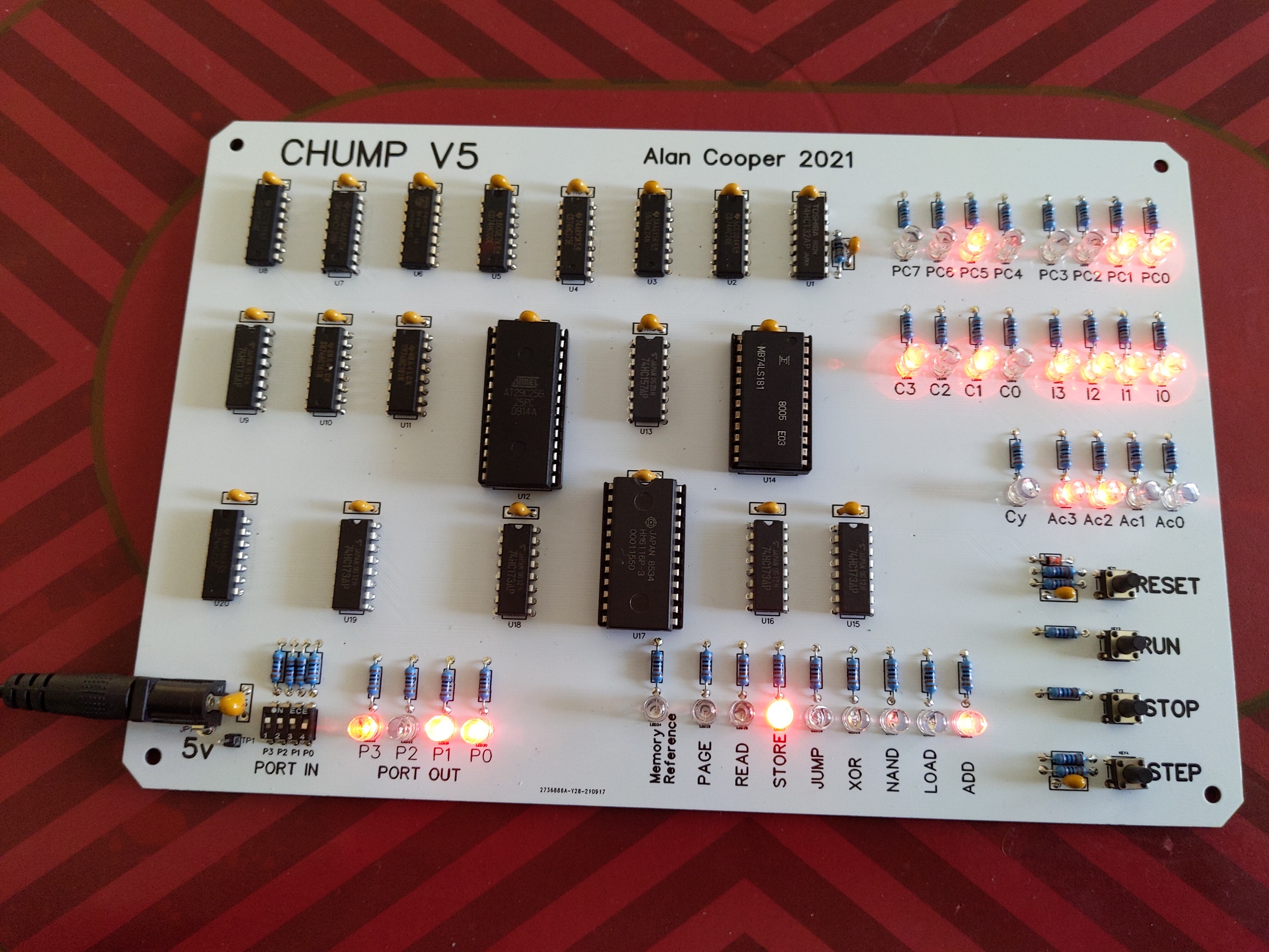
The PCB
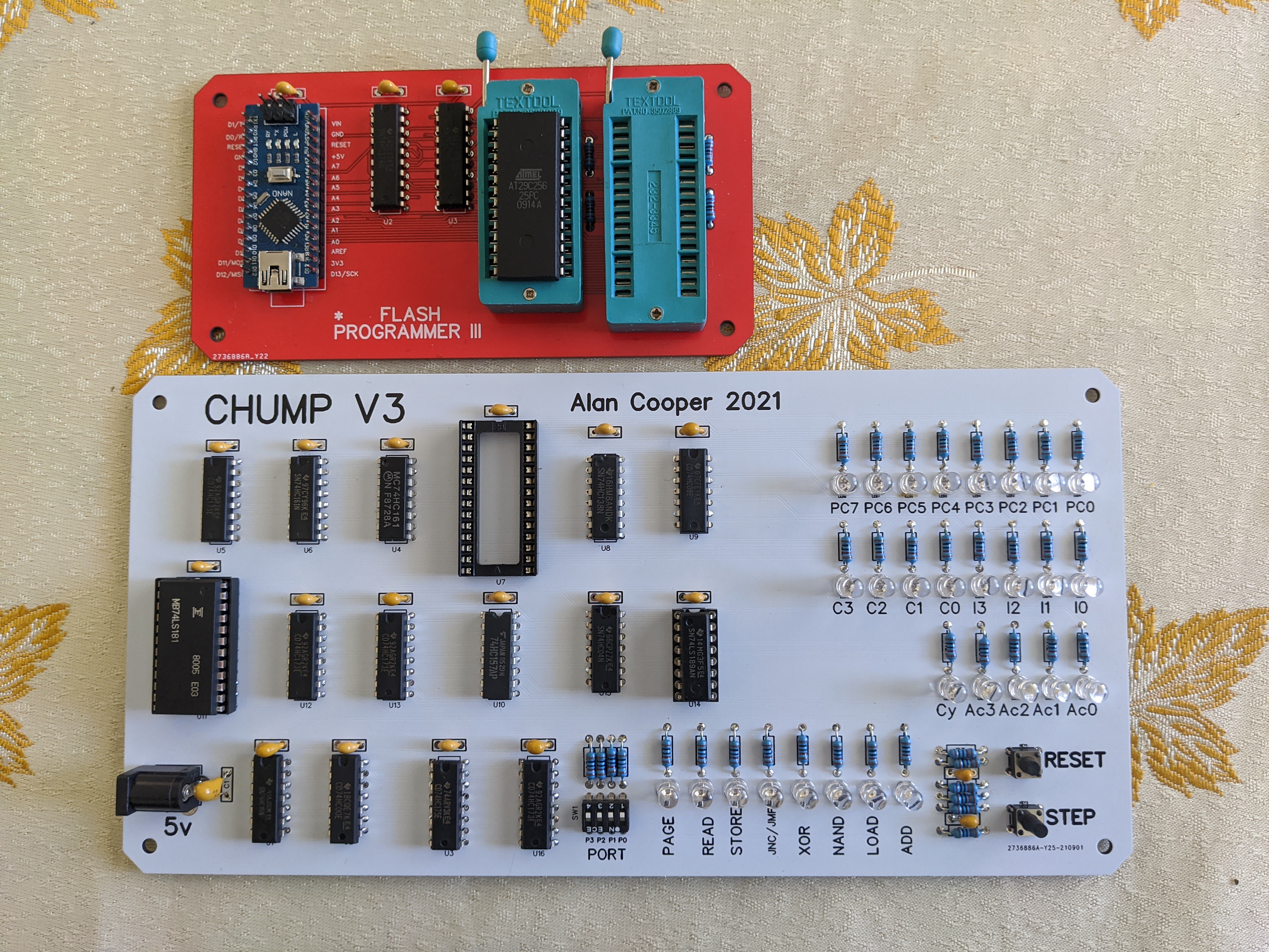
The PCB is now a little larger:
![]()
PCB Layout
The PCB is close to the point where the Easy EDA autorouter fails. I have a couple of strategies to extend the operational envelop of the autorouter:
- Adjust the track width (10 MIL) and clearance (9 MIL) to limit tracks between IC pins to one.
- Arrange the ICs to minimise connection lengths.
- Move ICs apart if track density is (too) high.
Assembly
Received the PCBabout a week ago. Assembled the PCB a few days ago. Wrote a test program this morning. Works fine. One minor problem was the Const/Inst labels are the wrong way around (I swapped the Const/Inst nibble order for V5).
![]()
Possible Upgrade
I think the ADD should be ADC (i.e. ADD with Carry) and the Carry should be persistent.
This would allow multi-nibble addition/subtraction without jumps. The carry signal can be cleared with "ADC 0".
Okay this project is done.
AlanX
-
Version 4
09/15/2021 at 23:47 • 0 commentsVersion 4
In version 4 I want to use a less aggressive memory write timing. Here is the updated Control logic:
![]()
Here I have done two things:
- The system clock (CLK2) is delayed 18ns behind the clock input (CLK1).
- The Memory WRite signal is ORed the clock input.
The results for the Memory WRite (!MWR) timing are:
- tAS (Address Setup time) is about half a clock cycle.
- tWR (Write Recovery time) is about 27 ns (before the rise of CLK2)
Replacing the 74LS189
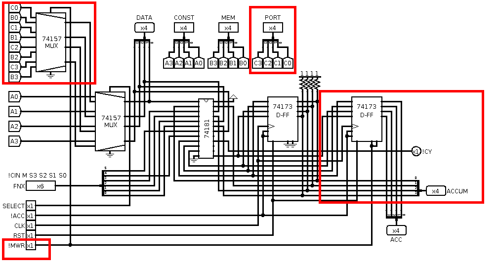
Replacing the 74LS189 with a standard Static RAM (SRAM) such as a 6116.
This requires a modification to the ALU to make the output tri-state and to directly select the Port bus:
![]()
There is also a new ACCUM bus so that the Accumulator can be monitored regardless of the output state of the ACC bus.
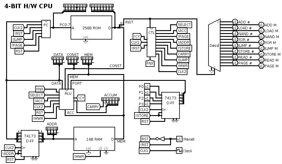
Here is the updated Top Level Schematic:
![]()
Upgrading the Clock
I want to upgrade the Reset and Step with Run (clock) and Stop (clock). The logic should be Reset and Step should stop the clock:
![]()
Note: I have added power on reset.
Note: The 7414/Or mess is actually one gate of a 74HC132 (Schmitt Trigger).
AlanX
-
Almost Works and Fake 74LS189
09/14/2021 at 00:17 • 3 commentsAlmost Works
The Monitor program almost works, but I have a memory read fault:
- LOAD 0
- STORE 1
- ...
- READ 1
- LOAD M
Should read back 0 (reads back B).
Likely my optimism for write timing was unfounded?
Strange I checked the schematic and I don't see any errors.
I checked the voltages on the 74LS189 pins (while stepping through the program) and they are a little strange. While MD can be tri-state, it was unexpected on D2 (around 2 volts).
I checked the power supply current which was high (267 mA).
I removed the 74LS189 and tried another, and then another chip without success.
I removed the 74LS189 and check the socket voltages (while stepping through the program) and they were as expected. I really cannot fault the board.
I checked the power supply current without the 74LS189 and it was quite reasonable (35 mA). How can the 74LS189 draw 232 mA and not destroy itself?
I checked the pin outs for the 74LS189 from another source, it matches. I am puzzled!
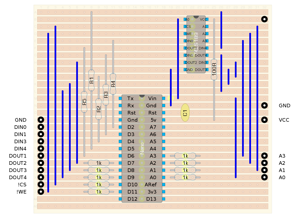
I have designed a Nano powered 74LS189 checker on vero-board, but I have no spare Nanos. I have ordered 3 but it will take two weeks to arrive.
![]()
Note: the 100R resistor is to limit power supply current to the 74LS189.
Note: the other resistors (all 1k), limit current to the pins of the 74LS189.
Fake 74ls189 chips
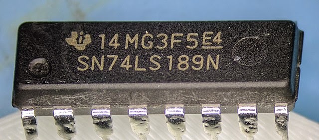
Last night while I slept I realised the only conclusion was that the 74LS189 must be a fake chip. This morning I found this post:
https://hackaday.com/2017/08/22/fake-ram-identifying-a-counterfeit-chip/
and
https://www.righto.com/2017/08/inside-fake-ram-chip-i-found-something.html
Here is what the fake chip looks like (mine are identical):
![]()
And the 10 chips I have are identical to the one shown in the posts.
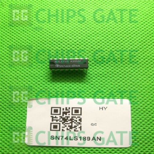
Rather than throw away the PCBs, I have order some more 74LS189. This time:
- the encapsulation is different
- the label is different
- TI does manufacture logic ICs in Malaysia
- there are similar chips with different manufacture dates on ebay, and
- they are from Hong Kong supplier rather than mainland China.
![]()
Hoping for the best.
AlanX
-
PCB Assembly and Monitor Code
09/14/2021 at 00:13 • 0 commentsPCB
I received the PCBs a few day ago and assembled one PCB yesterday:
![]()
I just need a monitor for the PROM.
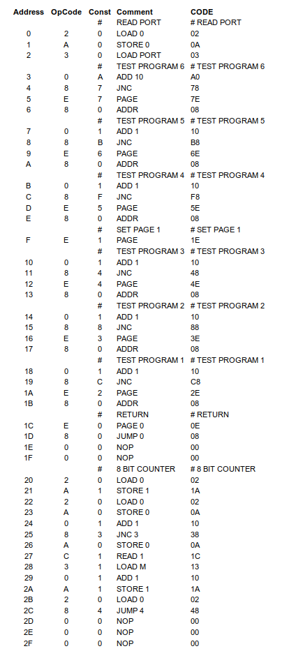
Monitor Program
The monitor program reads the PORT to determine which program to run:
- PORT 0: Read the PORT to determine which program to run.
- PORT 1: Program 1 -> 8 bit binary counter
- PORT 2: Program 2 -> Return to Monitor
- PORT 3: Program 3 -> Return to Monitor
- PORT 4: Program 4 -> Return to Monitor
- PORT 5: Program 5 -> Return to Monitor
- PORT 6: Program 7 -> Return to Monitor
- PORT 7-F: Return to Monitor
I have only one program at the moment, an 8 bit counter that uses memory address 0 for the low nibble and address 1 for the high nimble:
![]()
Update to LogiSim
The LogiSim model has been update to reflect the "As Built" more closely:
![]()
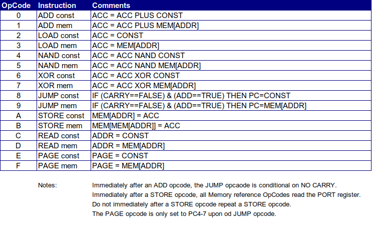
And the OpCodes:
![]()
Programming Experience
Compared to programming my TTA8 or SubLEq, this machine even with only 4 bits is a dream as the code density is so much higher (i.e. the number of bytes of code to perform an instruction, such as ADD). As instructions are one clock rather than eight clocks, it is also much faster.
What was I thinking when I designed the TTA8 or SubLEq!
AlanX
-
LogiSim
09/10/2021 at 10:57 • 0 commentsLogiSim
Decided to do a LogiSim for the design. About a day to put together the design and another day to debug the design:
![]()
The main problems discovered were:
Incorrectly modeled 74161 and 74173 in the library. This was a real pain because the models have strange behavour only in certain circumstances. In the case of the 74161 I fixed the problem, in the case of the 74173, I swapped it for a 74161 (just to get the simulation to work).
Another problem with the simulation is that tri-state logic often causes the simulation to start properly. The was fixed by using pull-up/down resistors.
Finally, my schematic looks good (just as well as the PCBs arrived this morning). The main issue is the Carry LED is rather confusing (I am not going to solder it in).
From a programming point of view, only holding the Carry for one extra cycle works for ADD but not for the composite SUB (i.e. NAND -1; ADD ?; NAND -1;). May be better to swap XOR for SUB in the instruction set.
Otherwise the simulation works as expected. So I have confidence that the PCB will be good.
AlanX
-
Control Logic Update and Added an Input Port
09/01/2021 at 03:23 • 0 commentsControl Logic Update
The STORE instruction does not update the the memory address. Here is an update of the Control Logic:
![]()
Adding an Input Port
It was noted that the STORE instruction sets the memory address when executed. The Accumulator is written memory during the next instruction. Therefore the instruction that follows the STORE cannot read the memory as the memory output is tri-state during a write.
I have taken advantage of this by reading a port during a memory write. Therefore an instruction that tries to read memory after a STORE instruction will actually read the port.
![]()
For this CPU, the user can store multiple programs and provide input to these programs.
The Accumulator can provide the output.
AlanX
-
Timing is everything
08/31/2021 at 14:54 • 3 commentsThe Static RAM Write Cycle Timing
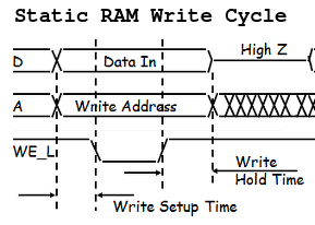
For static RAM, usually the write pulse starts after the address changes and write pulse finishes before the address changes to the next address:
![]()
The original CHUMP design uses a 74LS174 (Hex D-Latch) to clock each cycle, the memory address AND the memory read/write control. This works because most memory chips have a near zero "Write Setup Time" and near zero "Write Hold Time", AND the all the signals change at exactly the same time (as they are clocked by the same 74LS174 d-latch).
For my design I have separated the address d-latch and the read/write control d-latch. Therefore I have to ensure that both chips clock at the same time.
One problem is a slowly rising clock can cause the separate d-latchs not to clock at the same time. This has been eliminated by the use of the 74HC14 schmitt-trigger for the clock and reset circuity.
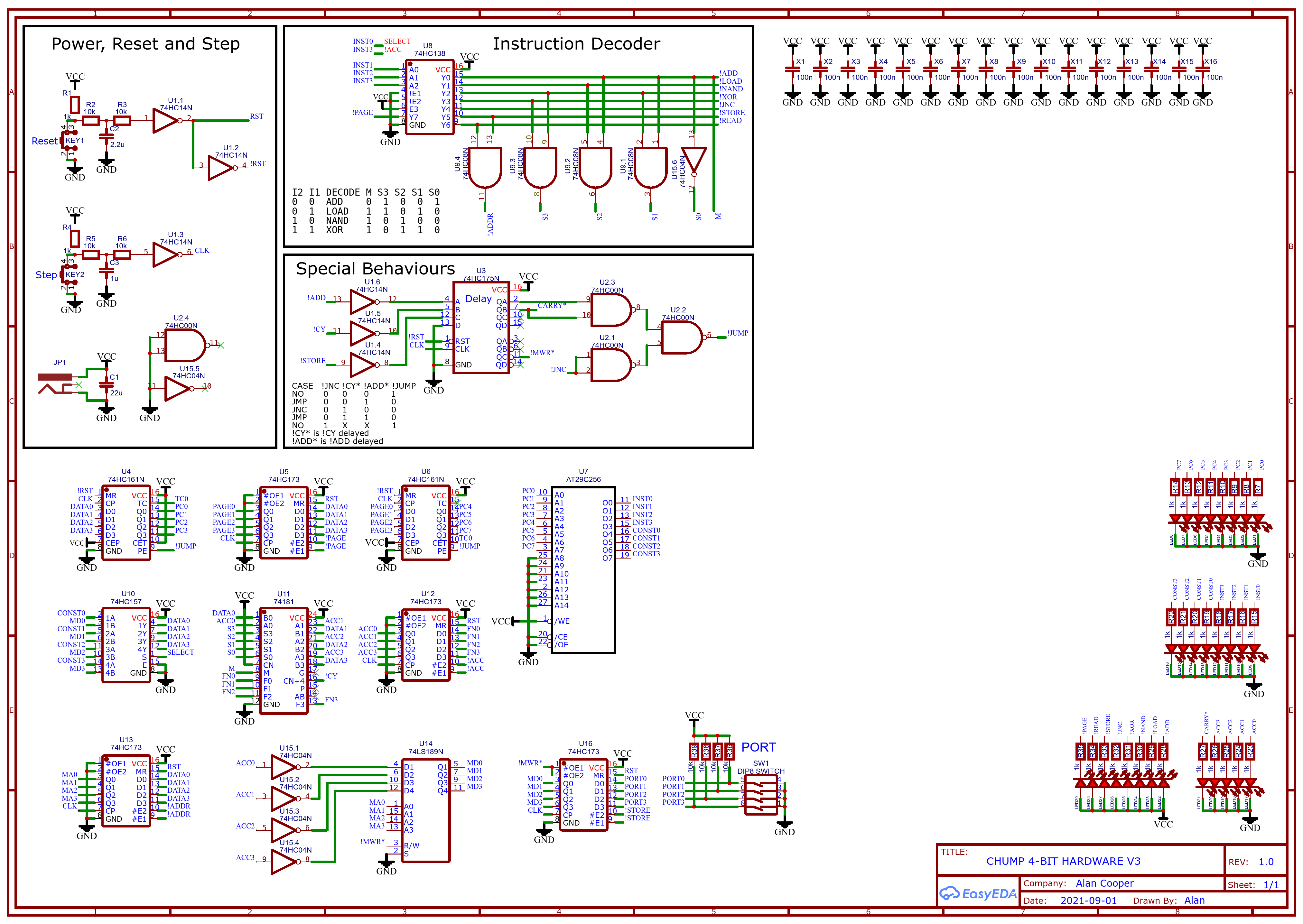
Another problem is a different propagation delay for the memory address and the read/write control. This has been minimised as both paths have the same (nominal) propagation delay (17ns), refer to U3 and U13, going to U14 in the revised schematic (around U3):
![]()
Finally, logic chips can tolerate small glitches if they are less than the propagation delay (say <8ns). This is based on the minimum clock pulse width of 7ns to 8ns for 74HC logic family.
An additional protection is that the 74LS189 memory chip has a typical 25ns minimum write pulse width.
AlanX
-
Control Design Logic - Logic Friday 1
08/31/2021 at 06:13 • 0 commentsControl Design Logic
Control design logic is a bit of an art.
Yes you can use a Programmable ROM or a PLA but for me, it more fun to use hardware logic.
Enter Logic Friday 1
Providing you stay within the limits of "Logic Friday 1", it is quite fun to use.
Create a logic table, solve the "sum-of-products logic expression" (i.e. minimise the logic equations/table) and export a minimised logic gate design.
For large tables Logic Friday 1 can import a spreadsheet CSV file.
For tables larger than what Logic Friday can handle, the underlying logic solver program "Espresso" can be used directly.
Worked Example
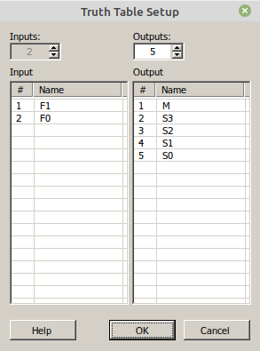
Consider recoding {M,S3,S2,S1,S0} to {F1,F0} for {ADD,LOAD,NAND,XOR}.
The table setup looks like this:
![]()
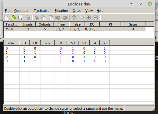
Next populate the table:
![]()
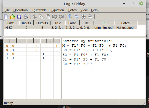
Next close the table and look at the pre-optimised equations:
![]()
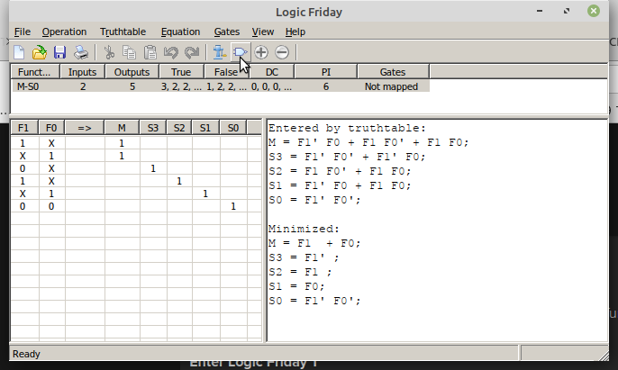
Now hit the "meat grinder" to minimise the equations, that is solve the "sum-of-products logic expressions":
![]()
At this point you could use the minimised table to design the logic gates directly say using a AND-OR PLA (Programmable Logic Array).
But for small problems it is easier to use the built in logic gate designer:
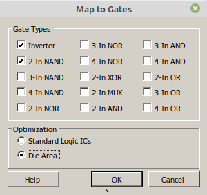
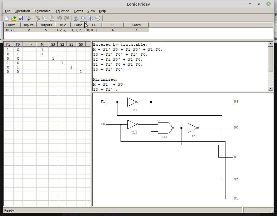
![]()
And finally:
![]()
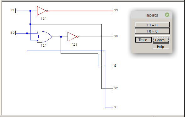
If you want you can check the design with the built in trace function:
![]()
Note: Blue is logic low and red is high high.
If you have not worked it out the last two schematics are functionally the same.
AND-OR PLA
PLA stands for Logic Gate Array and are usually configured as AND/OR logic. However you can also NAND-NAND (active high output) or NAND-AND (active low output) logic.
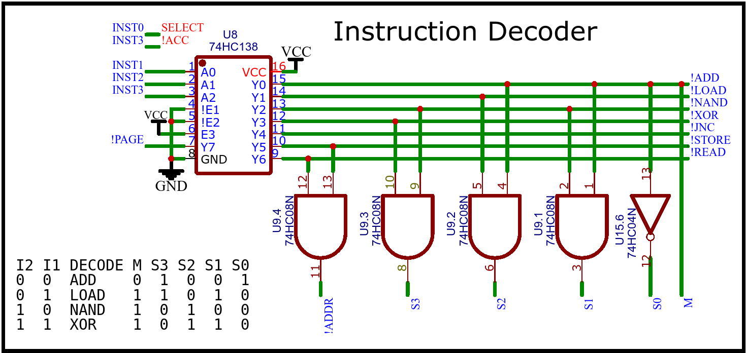
Here I use a 74HC138 to decode all the logic states (active low) for the Instruction Decoder. As I would prefer active low logic (to suit active low enable on most of the latches) for the outputs, I have used AND gates to decode the logic:
![]()
Note: I only decode I1/INST0 and I2/INST2 as I0/INST0 and I3/INST3 were trivial.
The 74HC138 approach can be expanded to suit more complex instruction sets.
Mapping the Jump Logic
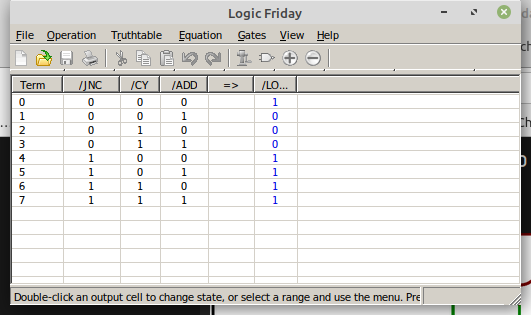
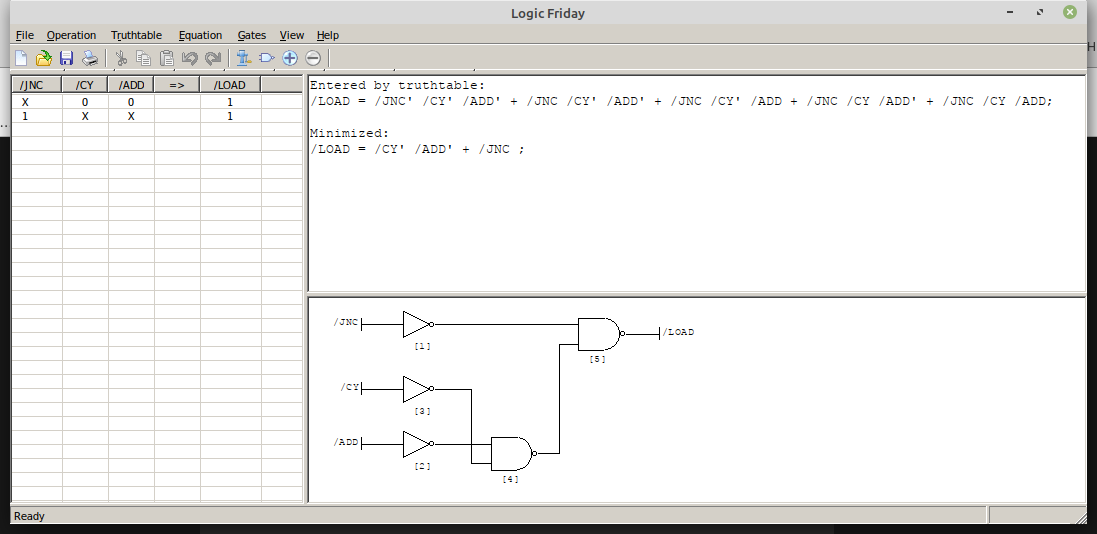
The jump logic for CHUMP was not immediately obvious, here is the truth table:
![]()
And the result:
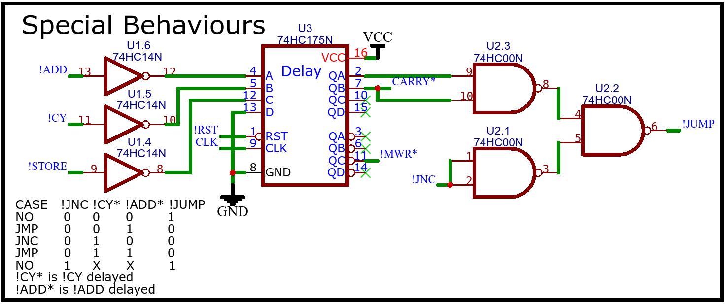
![]()
Okay, The jump logic is a bit more complicated in that !JNC is only active immediately after an !ADD, otherwise it should be treated as an unconditional jump (!JUMP). This is achieved by delaying !CY and !ADD with a clocked d-latch.
Here is the final schematic:
![]()
Note: For the delayed memory write (!MWR), the logic is inverted twice so that upon reset the default logic level is high (as the reset (!RST) clears (set logic low) the d-latch).
Hope this has been fun!
AlanX
CHUMP
CHUMP stands for Cheap Homebrew Understandable Minimal Processor. It is the invention of Dave Feinberg.
 agp.cooper