zpekic
-
Tracing and debugging for microcoded controllers
09/15/2021 at 07:13 • 0 commentsMore details coming soon. In the meantime, check out this teaser.
-
ser2par - a novel UART receiver (delay line approach)
09/15/2021 at 07:12 • 0 commentsRefer to the UART basics, and the component source.
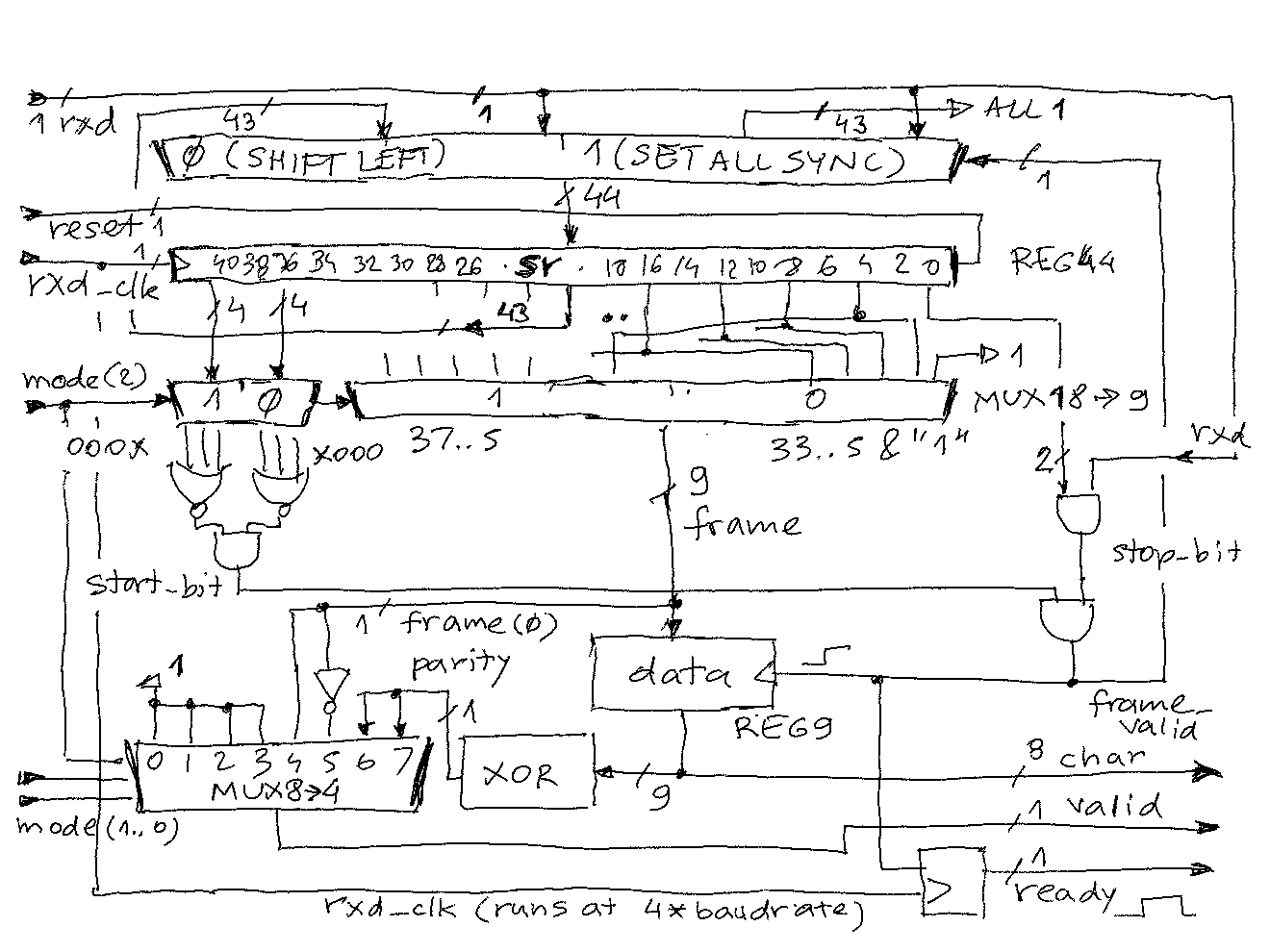
UART "receivers" that convert serial bit stream into parallel word and "done" signal are usually implemented as state machines. The trick is to observe the space ('0') state of the RXD input to decide if it is long enough to qualify for start bit, and determine the mid-point of the start bit to sample data bits at 1 / baudrate time intervals after that. Once the whole frame is counted, the state machine needs to be reset to initial state and watch for start bit again. There is some complexity to such state machine, which has to run over twice the frequency of the incoming data stream (sampling theorem), but in reality much faster, usually 4 or 8 times faster.
It can be simplified, and no state machine is needed, with a simple observation:
- if we have n / 2 + 1 mark bits ('1') in row (e.g. 3 for baudrate * 4), then it must be either a data 1, or a stop bit
- if at the same time, there are n / 2 + 1 space bits frame time in the past, then this must be a stop bit, and everything between is a data frame
With this, one has to simply have a 44 bit shift register (max 11 bits per frame supported * clocked at baudrate * 4), which receives RXD on the right (shift up), and simultaneously acts as a delay line. The stop bit is detected at the right side ("now"), and start bit at the left side ("past").
The operation mode is given by 3 mode bits:
mode data length parity frame length 0XX 8 none 10 100 8 space (0) 11 101 8 mark (1) 11 110 8 even 11 111 8 odd 11 The schematic below attempts to describe the circuit, which could also be constructed with less than 20 off-the-shelf 74XX logic IC.
- 44-bit shift register "sr" is driven by rxd_clk which is 4*baudrate. It has both async reset (at restart to set it all to "1", which will prevent error start bit detection (remember, start bit is "0"), and sync reset which must happen when a frame_valid signal is detected. Otherwise, it just shifts up the rxd input one place left ("shift up"). This means the more MSB the bit is, the more in the past it is. This is implemented with a register and dual input MUX. Note that at "sync reset", the LSB will be the rxd input to prevent loss of input stream during this moment.
- Given that this receiver supports 10 (no parity bit) and 11 bit UART frames (parity present), the start bit can be either at 43..40 or 39..36. That is the task of the upper MUX driven by mode(2). The lower MUX samples 9 bits out of the remaining 40 from sr, 4 bits apart, and close to mid-point of the bit time. When the mode(2) = 0 (10 bit frame), the LSB is forced to "1", otherwise it is picked up from sr register and represents the parity bit which is right before stop bit.
- The start bit detection works on the upper 4 bits of frame. To detect a "0", 3 contiguous bits out of 4 must be 0, therefore the NOR/AND generates "1" when start is 000X or X000.
- The stop bit detection works at the end of frame - 3 contiguous bits must be 1 - this includes 2 at the end of sr and the current rxd. This is a "look-ahead" that saves one clock time delay in the circuit.
- If the start_bit is 1 and stop_bit is 1, we have a frame_valid. This signal is used to capture the 9-bit (data + 1 bit parity) into the "data" register (so that the shift register sr can continue to run and capture the serial stream)
- 9-bits from the data register are fed to standard parity-generating XOR ladder. The upper 8 bits are presented to output as "char" parallel data, but with bits flipped (because of the order how bits are sent in UART protocol)
- 3 mode control input bits select the valid output signal, with modes 0XX always generating "1" because frame has no parity, while modes 1XX take the parity into consideration (NOTE: valid signal is not used nor was it tested in this design, may have bugs!)
- ready signal is frame_valid delayed 1 clock to ensure data register by that time already contains the stable data from the frame MUX. The ready will we 1 clock time wide pulse, and at can be used as latch, rising edge, or falling edge trigger to indicate to parallel receiver that char output has valid 8-bits from the UART frame.
![]()
-
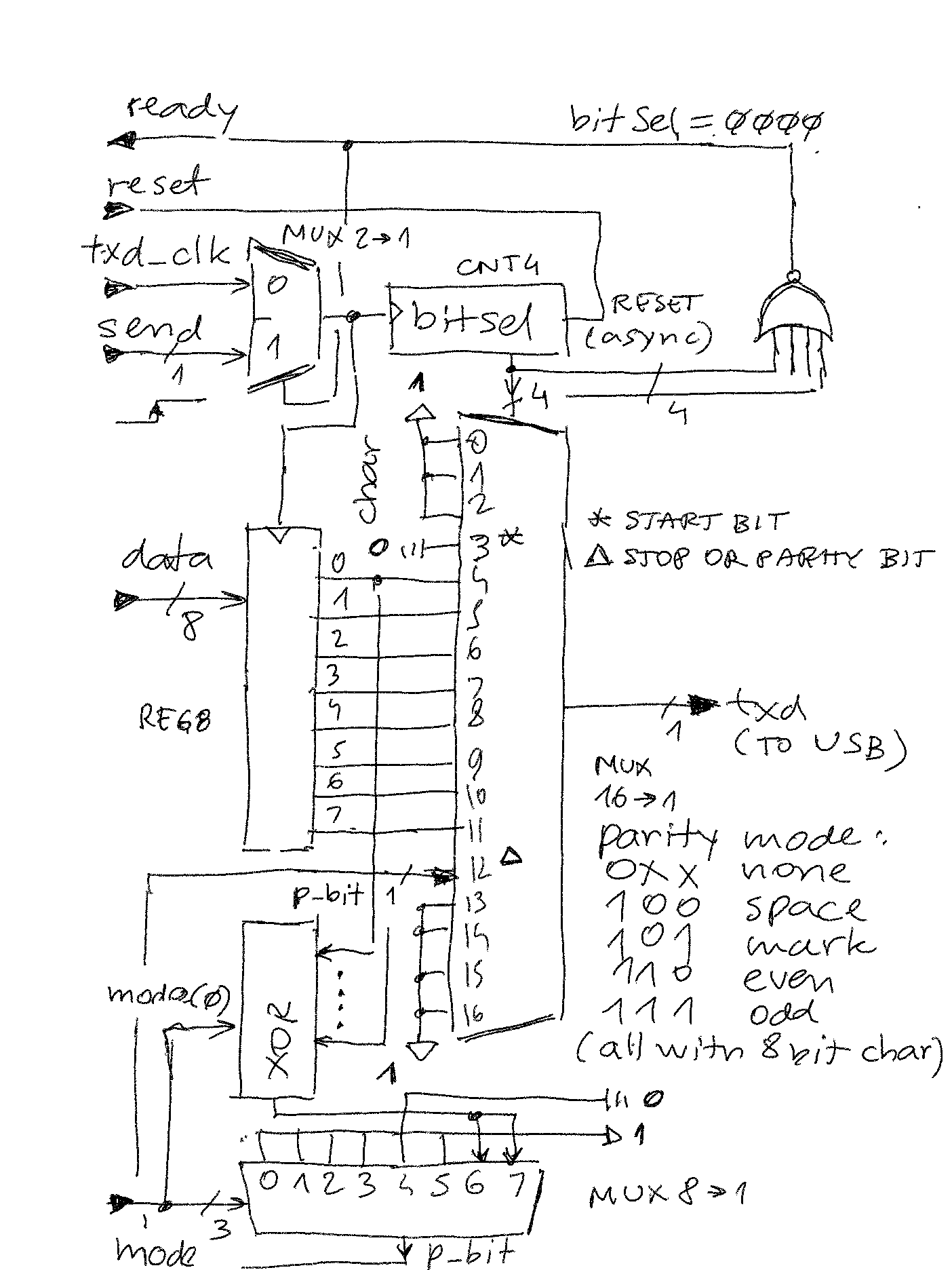
par2ser - a novel UART transmitter (counter driven MUX approach)
09/15/2021 at 07:11 • 0 commentsRefer to the UART basics, and the component source.
When it comes to converting parallel data to serial format, an idea of shift register comes to mind, and this is how often such circuits are implemented. However, with start / stop / parity bits, the shift register must be longer than the data, and with parallel data already buffered, the number of register bits doubles.
This component uses a simple MUX instead, and a 4-bit counter (bitSel). Operation is as follows:
- Reset clears bitSel
- if bitSel is 0000, the clock input is MUXed to "send" input signal
- external circuit presents data at the input and on rising edge of "send":
- bitSel is incremented to 0001
- char is loaded from data (input data is free to change after this)
- now that bitSel is != 0000, the clock is MUXed to baudrate
- as bitSel is incremented with baudrate frequency, the 16-to-1 MUX presents the right output to TXD (1, 1, 1, 0, char(0)... char(7)...)
- after char(7), the next bit depends on parity mode if selected
- finally a stop bit is transferred to TXD (this is simply MUX input driven to '1')
- when bitCnt reaches 1110, it is reset to 0000 and the circuit is ready from step 2 above
When bitCnt = 0000, it can also be used as a ready signal for the higher level circuit, meaning par2ser is idle and waiting to be loaded with data to transmit.
Main clock is baudrate * 1, which is the speed at which TXD MUX needs to change inputs. The operation mode is given by 3 mode bits:mode data length parity frame length 0XX 8 none 10 100 8 space (0) 11 101 8 mark (1) 11 110 8 even 11 111 8 odd 11 Here is a rough (but pretty accurate) sketch of the circuit. It could be implemented in less that 10 74XX TTL ICs.
![]()
-
mem2hex component - read from memory and generate .hex character stream
09/15/2021 at 06:57 • 0 commentsRefer to microcode and source code for the following description.
mem2hex is the simpler of two components. It is a linear memory reader, that adds some additional characters to the hex stream of memory bytes to produce a valid hex record. These records are 16 or 32 data bytes long, with the exception of last record which always has the same format (: 00 0000 01 FF)
Component structure (.vhd)
The main part are the registers that keep the state as the hex record is being assembled:
- mem_page, 3 bits long. This is the upper part of the memory address (A15..A13). It is handled separately to allow easy match with the 8 PAGE inputs to the circuit. Each of these independently enables generation of 8k block of memory as hex output. As the mem_page is incremented, a simple 3-to-8 decoder compares with current mem_page with the PAGE - if there is a match, the records are generated otherwise skipped ( page_match <= PAGE(to_integer(unsigned(mem_page))); ) . update_mem_page() process defines the operations on this register, and is simply clear, increment or stay the same
- mem_addr, 13 bits long. This is the lower part of the memory address A12..A0, that points within a byte in 8k block. update_mem_addr() process clears, increments or keeps this register same value
- checksum. 16-bit register that accumulates the checksum of each hex line. The value of this register updates at each clock cycle (lines 259 - 264), as a sum of checksum_r and checksum_s MUXs (line 280) which are both under microcode control. By default, checksum_r passes the register to one input of 16-bit adder, and checksum_s passes 0, resulting in no update. Other combinations cover address, data, complement etc. as needed to generate final checksum (only lower byte is eventually output)
- d, 8 bits long. This accepts the byte value read from external memory. update_d() process also allows this register to be loaded with constants 0 and 1 which are useful to generate the hex record, in addition to memory read and no change.
- count, 8 bits long. The update_count process updates this register by initializing it to 16 or 32 based on input pin COUNTSEL, decrementing it, or zeroing.
- CHAR, 8 bit long. This register holds the ASCII code of the character written to the output stream. The update_char() process allows it to be initialized with some constants (space, CR, LF, zero, colon) as needed for the record to be assembled, but importantly, it picks up hex to ascii conversion (4 bit to 8 - bit) through a lookup table (lines 79 - 95). The 4-bit hex value is selected by the MUX in line 332, which allows 4-bit chunks of registers to be selected for the stream, for example to generate XXXX address, 4 microinstructions are needed to drive the MUX with selections from A15...A12 to A3..A0.
Conditions: to drive the microcode logic, state of some registers must be detected, for example if count has reached zero, address / page is zero etc. These are in line 160...163.
Memory bus interface: this is a "Z80" - like interface. mem2hex behaves as a DMA-output device:
- nBUSREQ output is asserted low to demand bus
- nBUSACK input is read, and if low, means mem2hex can access bus, otherwise there is indefinite wait until this signal goes low
- nRD is asserted low to initiate read
- ADDR is driven by page and address registers
- nWAIT is read during bus read cycle, if found low, cycle is repeated, and when high, next clock transfers DBUS to d register
- when nBUSACK is low, nRD and ADDR are enabled, otherwise they are tri-state. This allows connecting these signals to common system bus
Code structure (.mcc)
Microcode starts with the definition of storage and controller unit:
.code 6, 34, mem2hex_code.mif, mem2hex_code.cgf, mem2hex_code.coe, m2h:mem2hex_code.vhd, mem2hex_code.hex, mem2hex_code.bin, 8;
.mapper 8, 6, mem2hex_map.mif, mem2hex_map.cgf, mem2hex_map.coe, m2h:mem2hex_map.vhd, mem2hex_map.hex, mem2hex_map.bin, 1;
.controller mem2hex_control_unit.vhd, 4;
This defines:
- controller with 4 level deep stack (current + 3 subroutines deep max)
- code memory (microcode) 34 bits in width and 64 (2^6) words long (for padding, 8 bytes will be generated per word. m2h prefix will be used to differentiate from other possible files with same names in the project)
- mapper memory of 256 locations of 6 bits (usually mappers translate from instruction register to entry point in the microcode implementing that instructions, but in this case the "instruction" is the PAGE input which can be any of 256 combinations of enabling 8k block memory to be output or not. The special value 00000000 means only the hex file last record will be output). 1 byte will be used to round up the padding (as the values are just 6 bits)
After these, the fields in the microcode must be defined:
- regfields - these are assigned with <= in the microcode and indicate state will be captured at NEXT ACTIVE microcode clock edge
- valfields - assigned with = in the microcode, and indicate that the value will be held DURING CURRENT microcycle.
- if field - can occur only once and describes valid conditions to use for branching. Usually true and false (always and never) are included for convenience.
- then field - valid branch destinations. Control unit is hard-wired to recognize first 4 values as next, repeat, return, fork
- else field - same as above
Alias definitions are convenience to minimize coding repetion. They are simple forms of "macros".
//	useful aliases, these are evaluated as simple text replacement of label with everything between .alias and ;
goto:	.alias if false then next else;
noop:	.alias if true then next else next;
back:	.alias if true then return else return;
with the above, writing "goto foo;" is a simple jump, and writing "back;" is unconditional return from subroutine etc.
Subroutine definitions:
The controller unit is wired to check the then and else part of the sequence and if they are same and not one of the first 4 reserved values (next, repeat, return, fork), branch to that location but pushing the current address + 1 on the stack. This is done in 1 cycle. There are two ways to achieve this in the microcode:
- use .sub pragma with label defined by it
- use "if condition then label else label" (which can be shortened as .alias)
#1 is preferred because is allows listing any number of regfield name definitions. These are not true "parameters" but handy way to indicate which register values will be set as the subroutine starts executing.
(to be continued)
-
hex2mem component - accept .hex character stream and write to memory
09/15/2021 at 06:55 • 0 commentsRefer to microcode and source code.
This component has the following capabilities:
- Accept ASCII characters on its 8-bit write-only port with simple handshake logic (it can interface with an UART to accept serial stream from host computer)
- Interpret incoming character stream as records in Intel .hex file format
- If the record received is valid (no bad characters, right number of bytes, good checksum), write the record to memory
- Memory interface is 16-bit address, 8-bit data, and using DMA logic similar to Z80 (BUSREQ - BUSACK)
- Signals error on a dedicated pin
- Provides a debug serial port to trace execution of the internal microcode
Intel HEX files for FPGAs (no embedded CPUs!)
Uploading / downloading Intel HEX file stream during system runtime, implemented without embedded processor!