 Rudraksha Vegad
-
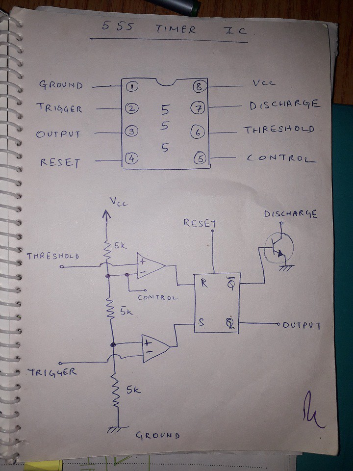
1Understanding the Basic building blocks of the 555 Timer
Block diagram of the 555 timer.
![]()
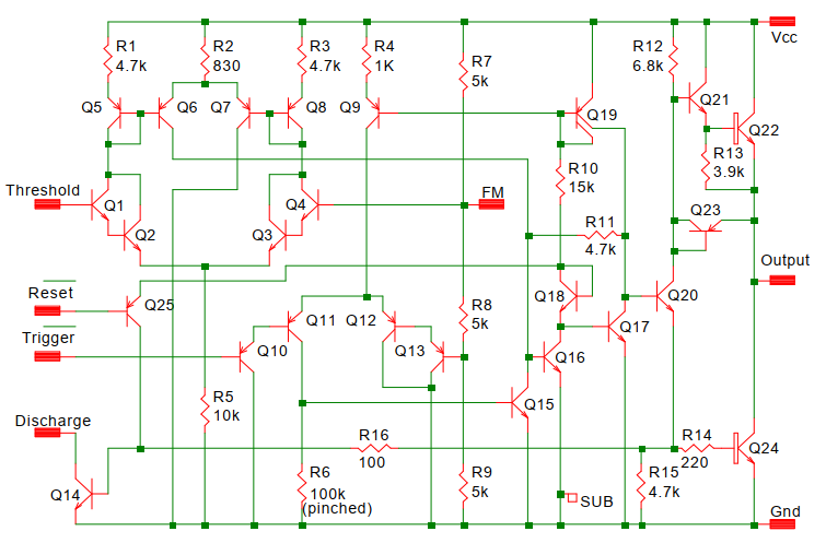
Below is the original Component level circuit of the 555 timer designed by sir Hans Camenzind
( not my circuit )
![]()
image taken from Tiny Transistors website I will modify the above circuit and optimize it for discrete components
If we look at the above circuit which is the actual circuit of the 555. But when tried to reverse engineer it and try to understand it , first off all its very confusing, I mean why using two different types of comparators one NPN based and other PNP based.
So I decided to ignore the 555's original circuit and learn the fundamental blocks of 555 form scratch and redesign it for discrete component form.
The first and the most important circuit of the 555 is the two voltage comparators. Which brings me to step 2. understanding the differential pair.
-
2The Voltage comparators
Reference - For designing these differential pairs to serve as a very basic voltage comparator i found a gem on YouTube for understanding the internal working of Op -amps and fundamentals of differential pair - w2aew YouTube channel video on long tailed pairs. ( Not my video/Channel ) . He also has many fundamental videos on electronics for any beginner like me . Very very nice channel on YouTube ,his way of explaining things is just outstanding and very different.
Firstly I grabbed some random NPN transistors form my parts bin and just tested the behavior of the simple long tailed pair - in this case used some S9013 NPN BJTs
I used NPN because I am much more comfortable working with NPN designs
![]()
I was surprised at the common mode input response. The output was quite balanced but not as good as a real op amp.
Even if the two transistors are not matched ,as per my experimentation on breadboard it works fairly well as a voltage comparator and we only want to use this circuit to operate so that it slams the power rails 0V and the supply rails ( Digital output ) so matching here doesn't make any significant difference. ( But for analog application it is a must to precisely match those transistors.)
So if you plan to build a DIY voltage comparator out of discrete components it is not important to match the diff. pair transistors.
But there are many problems in the above circuit -
- Output doesn't remain stable if common mode level is changed. Also by varying Vcc the steering current changes.
- The gain of the above long tailed pair is low
- input impedance is very low
- No single ended output
Lets solve them one by one-
-
3Adding a Constant current sink instead of tail resistor
![]()
Here I used a classic BJT constant current sink instead of the tail resistor. in this case about 1.5 to 1.7 mA tail current depends how the BJT is biased.
After the constant current sink the input impedance got slightly higher that is what we want.
Also by changing common mode level the output is slight more stable than before.
And as a plus point by varying Vcc the steering current remains constant.
-
4Adding more gain using Current mirror
![]()
Replacing collector resistors with current mirror greatly increases gain.
Now when I was designing the circuit and learning how it works I know what current mirror does, but here the way the current mirror is arranged is a bit confusing but later diving deeply and understanding , I got what the mirror is actually doing over there.
Its basically reinforcing the "resistor pull up effect" which earlier collector resistors did. It drastically saturates the output even with few millivolts difference in the two input voltages.
Here's how it works:
Say left NPN BJT = Q1 and the right NPN BJT = Q2
Case 1:
Lets assume we put 2 volt on the Q1 input and 1 volt on Q2 input.
Q1 will be turned on harder than Q2 which will drop voltage at the collector of Q1 which is also connected to the bases of current mirror. Since the current mirror are PNP the low voltage at its base will turn them on ( in this case will mostly saturate ) .
Now voltage at the collector of Q1 will still remain low but now since the current mirror is in action the same current flowing through Q1 will also try to flow through Q2 but Q2 is off mentioned earlier.
But the mirror will still force and try to give the same current to Q2 but Q2' collector Blocks that current . Therefore voltage at collector of Q2 rises drastically . That is, output is high.
Case 2:
Lets assume we put 1 volt on the Q1 input and 2 volt on Q2 input.
This time Q2 will be turned on harder than Q1
Now in this situation the mirror will be kind of disabled - because the bases of the current mirror is floating ( not at any voltage neither Vcc nor GND ) this is because since Q1 is off and therefore Q1's collector is disconnected from Vcc at this moment . We know Q2 is on therefore its collector is grounded therefore output is ground.
It can clearly be seen that left input is Non inverting and right input is inverting in nature.
As plus point now our circuit has converted from differential output to single ended output which is with respect to ground. which is what we wanted.
-
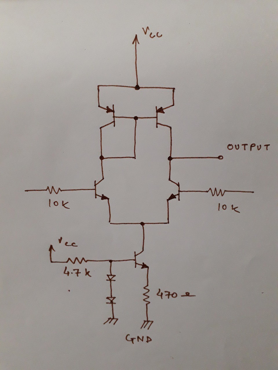
5Improving input impedance
Increasing the input impedance and further improving the gain using Darlington inputs
![]()
After adding the Darlington inputs the input impedance is greatly increased. You can also see that the 10K input resistors are now replaced with 150 K resistors.
I have tested and i can say 1 M ohm resistors can also be used but then somehow the circuit becomes very slow in response to input voltages so around 100K to 470K is enough and works fine.
-
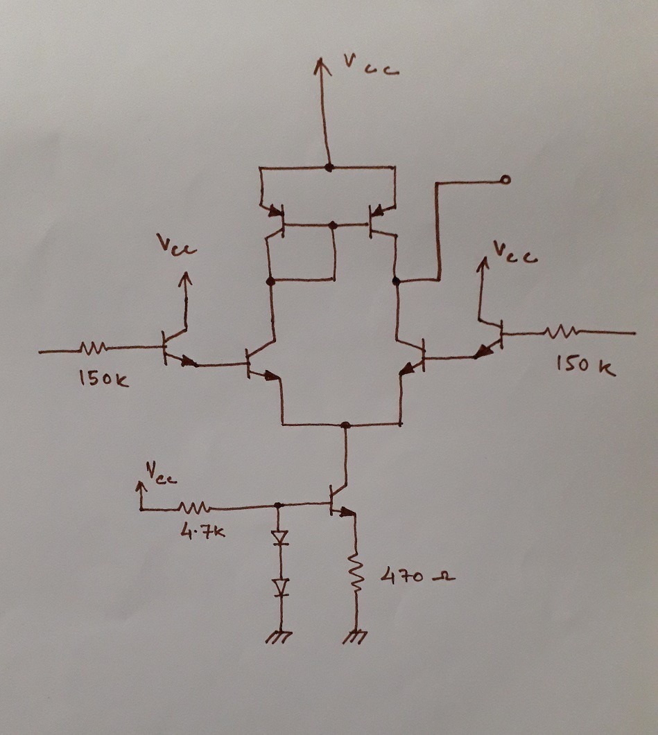
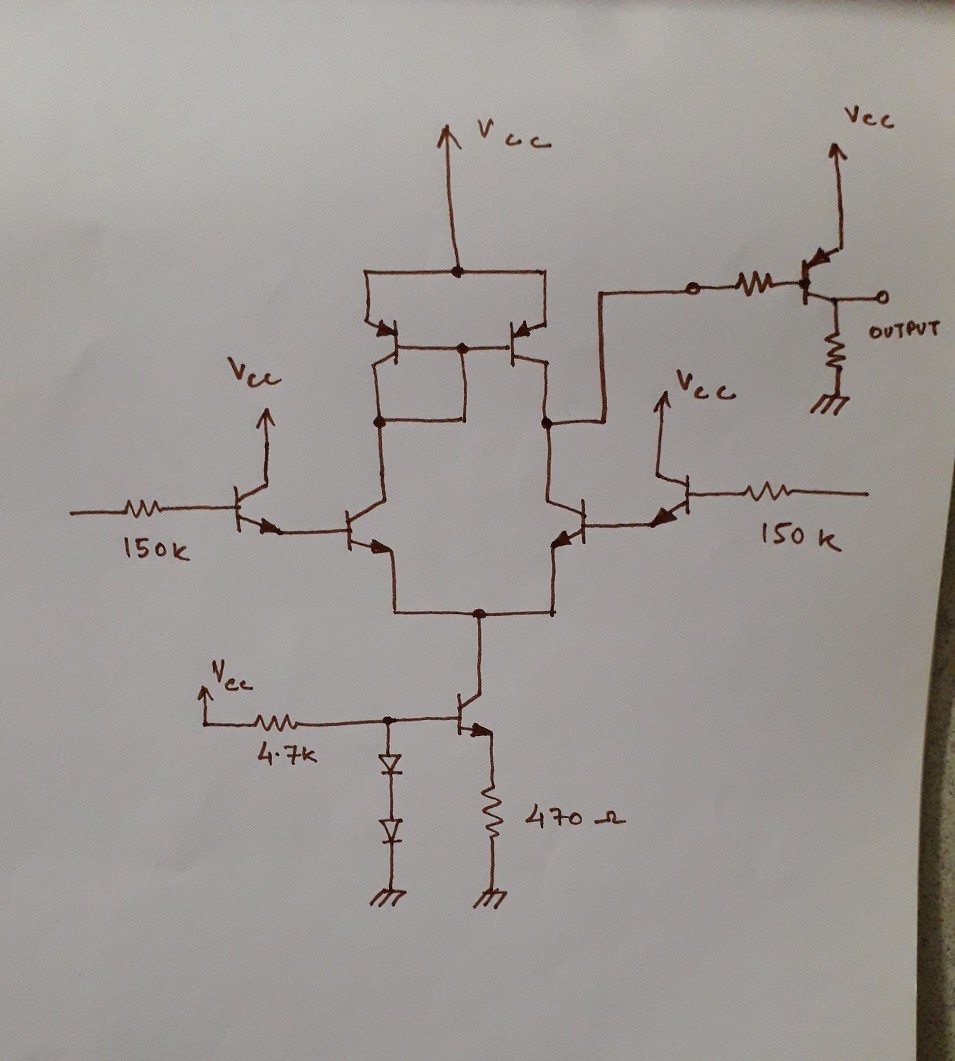
6Improving the output stage.
At this point the voltage comparator is working well but there's a small problem, the output voltage is much more like a op amp rather than a comparator with a sharp voltage transition and is little bit inconsistent I mean sometimes the output reaches close to Vcc and then with different input voltages the output may be 1 or 2 volts less then Vcc. but it very nicely reaches to ground. I searched about this problem but I couldn't figure out what was the issue but then stumbled upon a Instructables page about discrete 555 timer and its details.(not my page) and saw some handdrawn schematics and notice the out stage should have a PNP transistor. Then i realized that a lot of datasheets have this.
![]()
By adding a PNP transistor the out voltage transitions more sharply and also it can reach very close to Vcc as well as complete ground. I Think this is because earlier i mentioned (that output can reach to ground.). Now the PNP solves the inconsistent Vcc output.
This is the final circuit shown above for the voltage comparators that i have used in the 555 circuit . It works pretty nice and i think no other modification is required at this point.
Also I would like to mention that I have used This exact circuit for both the comparators - The Threshold and Trigger comparator. In the original 555 circuit they used a NPN style comparator and a PNP style comparator. I don't see any reason for doing so. therefore I used to identical comparators based on NPN design.
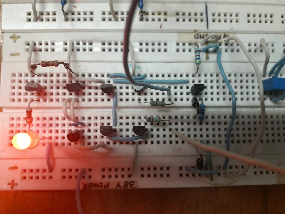
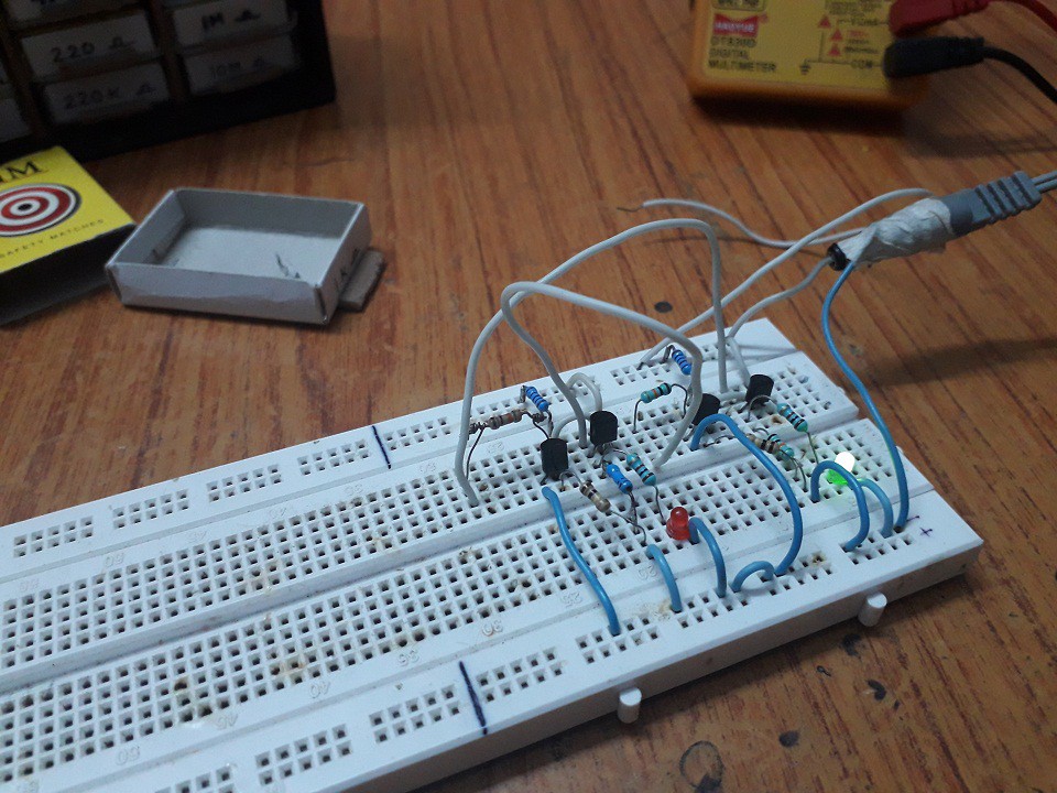
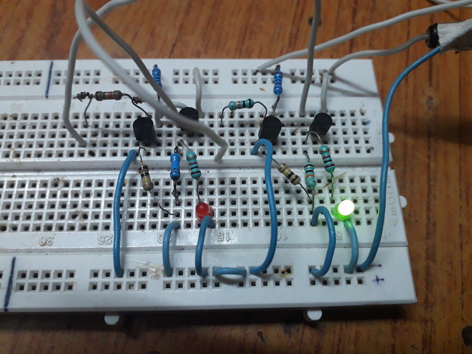
Testing on breadboard:
![]()
![]()
![]()
-
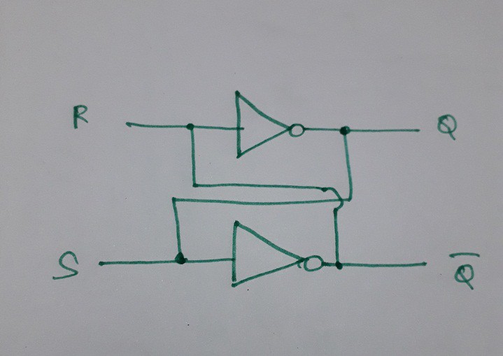
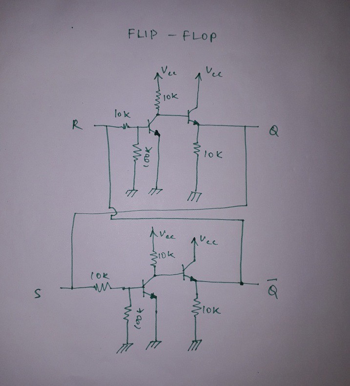
7The SR Flip - Flop
For the SR flip - flop I used classic two transistor flip - flop along with that with some simple BJT output buffers to decrease output impedance of the flip - flop.
![]()
![]()
As you can see I have added output buffer for Q and Q~ outputs.
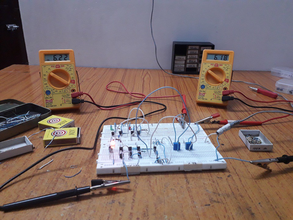
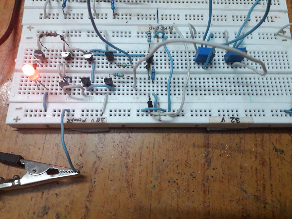
Breadboard testing:
![]()
![]()
-
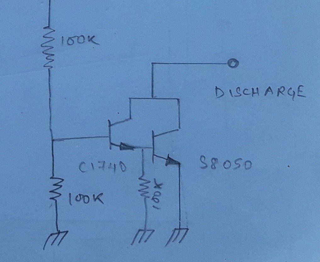
8The discharge Transistor
![]()
Here I have used Darlington pair for discharge to make sure that the discharge transistor turns on "hard" and completely connect to ground.
-
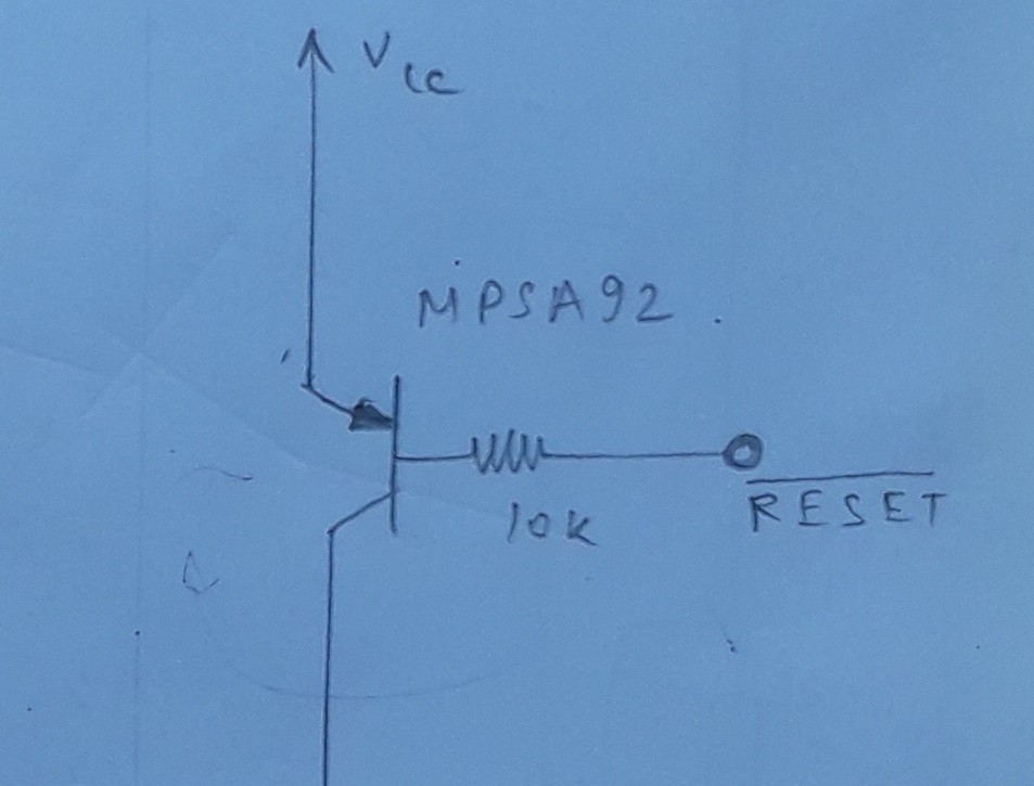
9The reset transistor
![]()
-
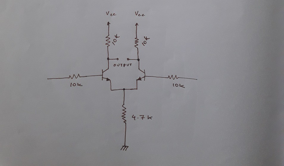
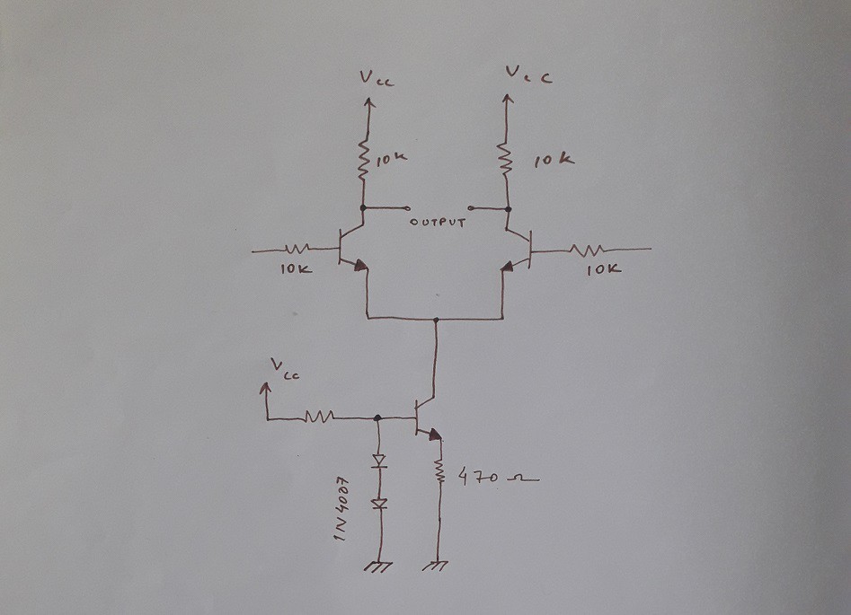
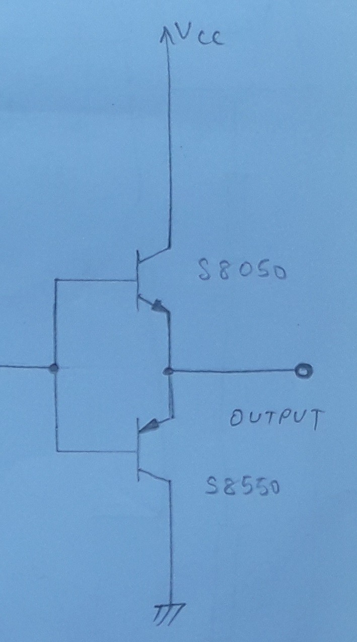
10The output buffer
![]()
In the original 555 circuit they use totem pole circuit for the output but it was a little confusing so I used the simple push - pull arrangement for output buffer.
Giant 555 Timer
A Working Replica of the classic 555 timer made using discrete components
Discussions
Become a Hackaday.io Member
Create an account to leave a comment. Already have an account? Log In.