-
build log 7 - SRAM / ROM / serial
01/08/2022 at 14:34 • 0 comments![]()
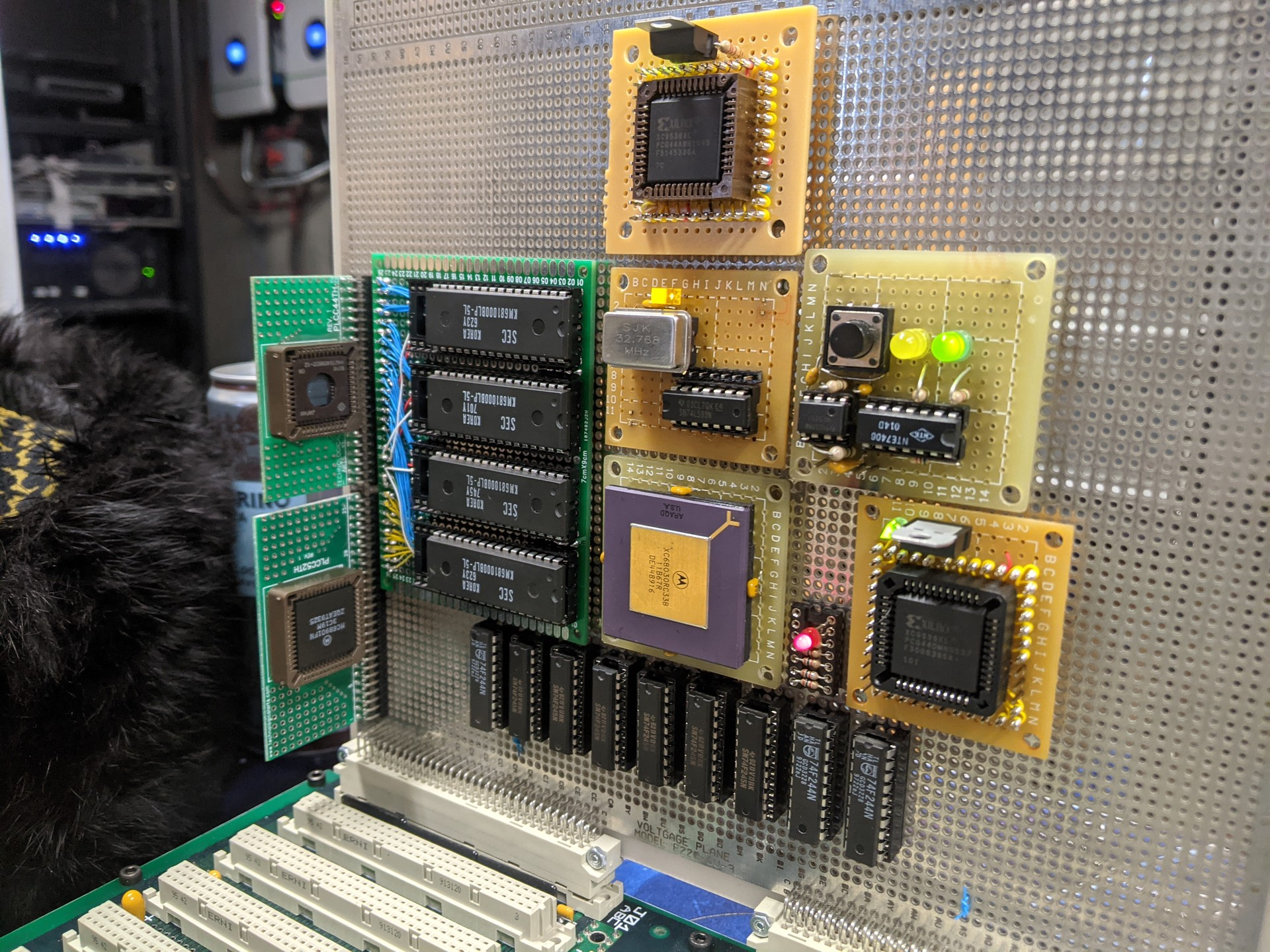
512KB 55ns SRAM added
512KB ROM added
MC68901 Multifunction Peripheral added
The CPLD at the top is a 7ns part and is tasked with address decoding and chip select generation. The CPLD on the lower right is handling the VMEbus signal synthesis and is additionally dealing with the interrupt signals.
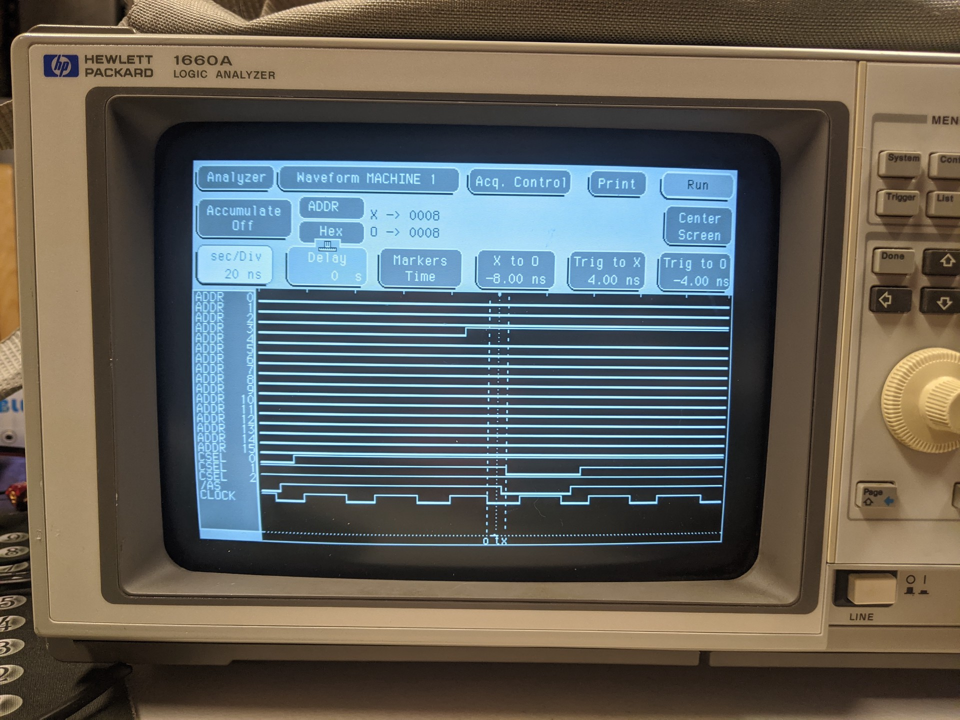
Initially I had concern that the CPLD would not be fast enough for address decoding, but it seems to be doing the job. My logic analyzer only runs up to 500MHz, so 2ns is my resolution, but the CPLD is driving the chip select low within 2ns of the address strobe being asserted.
![]()
In this capture, ADDR3 through ADDR 15 is attached to A19 through A31 on the CPU. CSEL 0 is ROM and CSEL 1 is the MFP chip select. As expected, the CPU transitioned from asserting ROMCS to asserting MFPCS when A19 went high. The time between /AS being asserted and MFPCS being asserted was within 2ns. The only think keeping me from running this thing at 0-waitstate is the fact that my pokey SRAM is only 55ns. I have faster parts on hand, but i will need to make a PCB for those as they are surfacemount components.
-
build log 6 - ROM, basically
12/24/2021 at 07:50 • 0 commentsmy apology for lack of updates... got a million things in flight IRL at the moment and very little cache to deal with them all...
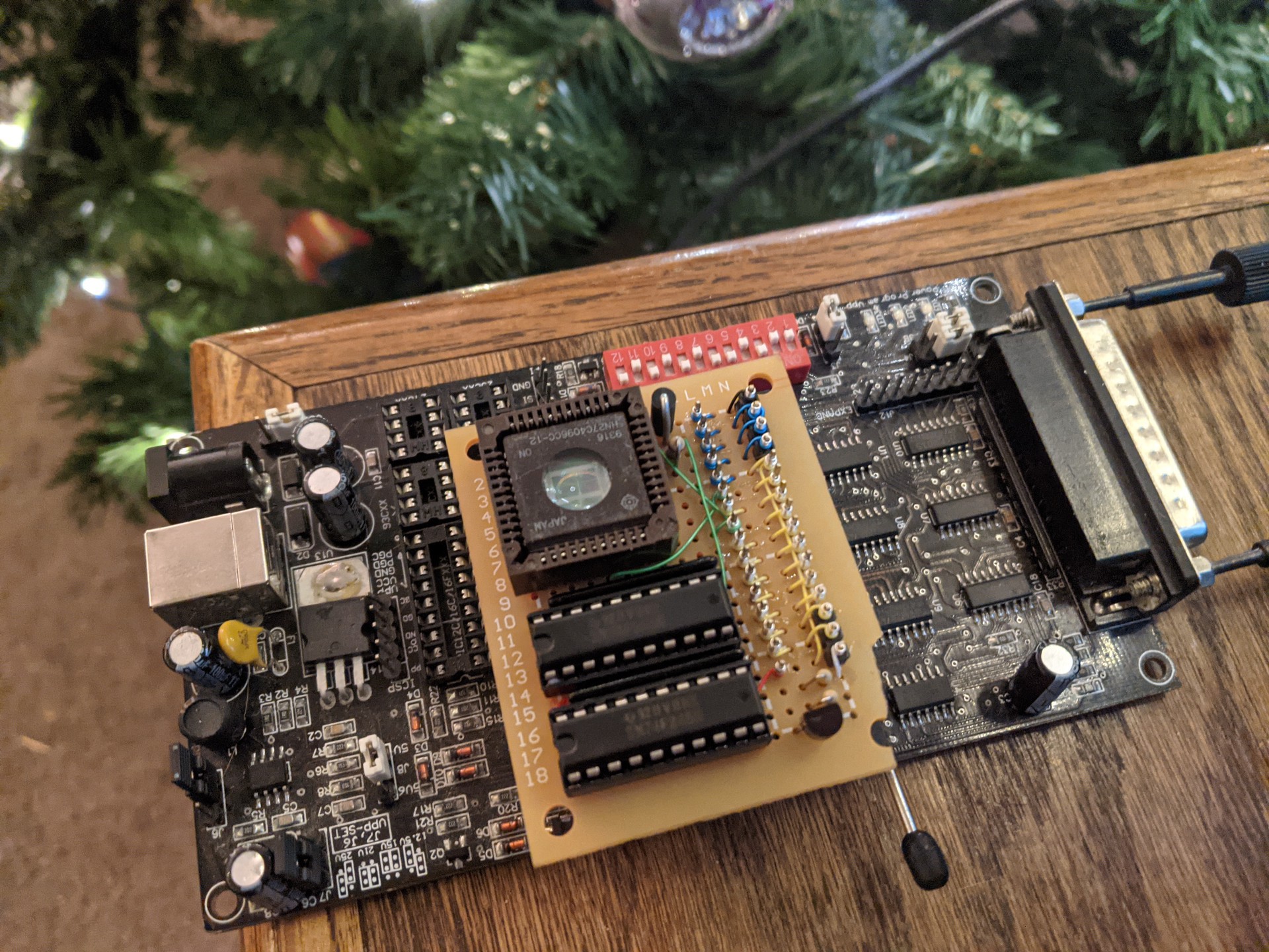
i needed to get ROM and SRAM attached to hexahedron, so i built a wirewrap adapter for the PLCC44 ROM that I have. around that point, i realized that my ROM programmer is only good for 8-bit ROMs. No problem, I can build an adapter...
T W O H O U R S L A T E R![]()
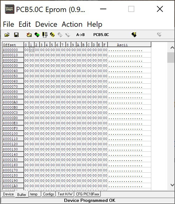
I threw a test pattern at it... 0xAA55... and it worked... GREAT!
...or not. When I decided to fill the thing with `0x00000000`, you know, for that sweet `ORI.B #0, D0` free-running code, i realized that it was returning 0x80408040. obviously two of my data lines were not properly connected. after throwing another half pound of solder on the back of the adapter, all was well...![]()
unfortunately, now i have to handle a few non-maskable interrupts in real life, so i won't be able to test the free-running from the ROM until tomorrow. i will, however, share the schematic in a few minutes showing my idea for jumperless IO base address configuration.
-
build log 5 - unorthodoxy exemplified
12/14/2021 at 05:58 • 1 commentcurrently programming the PLDs for the system. while doing so, i started thinking about how i wanted to handle the memory-mapped IO, and how to remap peripherals. sure, i COULD do it old style and use jumpers to set a comparison address on a 74F521, but that seems entirely too pedestrian for this project. i like the idea of setting things in BIOS, interactively...
...the problem is, HOW?
seems like there are plenty of motherboards that I have owned, even back in the 80386 era, that were jumperless and permitted changing the base IO address of serial and parallel ports. i never really looked into how this was accomplished. this isn't really something that is easily searched for either, and no magic combination of search terms led me down a path to illumination.
so, i decided to get creative...
hexahedron will boot up with ROM at 0x00000000, but this can cause issues with linux, issues which have workarounds, but issues where remapping the base IO of ROM will be useful. the ROM that i have on hand is a 4megabit (512KB) HN27C4096CC-12, an aesthetically pleasing piece of silicon for sure. the idea is to have a 74F521 attached to 8 lines of the address bus for each peripheral (RAM, ROM, serial0, serial1, parallel, etc). instead of front loading these with jumpers to set the identity address, i will be using 74LS164 shift registers... shift registers and a microcontroller.
the microcontroller i have on hand is an ATMEGA328P. it will have it's own 74F521 and 74LS164 as well. it will have one line running out to gate each of the 74F521 outputs, except for ROM, which will be on its own dedicated pin which will be asserted (LOW) at power-on. at power-on, each of the 74LS164s should have their outputs = 0x0000, but only ROM will be enabled so the CPU will start reading from ROM as it loads BIOS. meanwhile, the microcontroller will run through its own internal program, reading the base IO address stored in EEPROM for itself and each peripheral. by default, the MCU will have 0x80000 as its base address, residing just above the ROM. it will then serially clock in data to its own shift register so it will match on 0x80000, and then it will proceed to do the same for the other peripherals. once they are all set, the MCU enables output on the non-ROM ID comparators.
the CPU will then contact the MCU at 0x80000 and request the peripheral base IO addresses stored in its EEPROM to update its own state. at this point, the user is free to remap the base IO address for anything by sending commands to the MCU, eventually disabling the ROM and remapping RAM to 0x00000000 should the need arise.
at this point, some people are either facepalming over my overcomplication of matters, or amazed by this implementation. maybe i'm doing something that is actually sane. i don't know, but i have to try it at this point. feel free to chime in if you have insight as to how jumperless motherboards actually work on commercial gear. -
build log 4 - VME basic connectivity
12/12/2021 at 13:33 • 0 commentsin this build session, i rewired the entirety of the computer, primarily to relocate the CPU module and make room for the bus transceivers. most of the other systems that i have seen are using 74LS645s for the bus transceivers, perhaps because they can sink more current. from a previous conversation on my rhombus project, it was mentioned that up to 64mA would be needed. i do not have 74LS645s on hand, however the 74F245s that I have will sink that much, with the caveat that it is the B port, not the A port. as a consequence, i have the CPU attached to the A side and the bus attached to the B side. this will require inverting the chip enable logic, but seeing as this will be handled within my CPLD, i suspect that it will not be an issue.
speaking of the CPLD, after obtaining an XC9536XL, my programmer worked just fine. the only issue here is that i'll need a 3.3V supply for the CPLD's main source, but the I/O is rated to handle 5V.
video 1: overview of current state
video 2: added the address lines A24-A31 to the bus and added LEDs to visualize the activity
-
build log 3 - revenge of the part obsolescence
12/08/2021 at 17:09 • 1 commenti am rethinking a few things regarding this project. i would prefer to use programmable logic, but i would also prefer to avoid using level shifters to deal with the 5V logic on the CPU and other peripherals. the xilinx situation has been a bit of a fiasco, and i will elaborate here.
to program the CPLDs that i have, i had to build a programmer since the one that i used with rhombus would not work. i built 3 programmers, one of which was a parallel port design published by xilinx. none of them worked reliably. long story short, the newer versions of the xilinx software do not support the revision 0 silicon that i have. i suspect that the commands are similar, if not identical, however i cannot program the CPLDs. the CPLD has a different device id and the first 4 bits indicate the revision and are '0' instead of '2', thus the resulting .svf and .xsvf files will not work. i attempted to modify the .svf, which is human readable, to updated the device id, and this permits the programming to proceed a bit further, but it still fails due to intermittent mismatches coming from the chip. i triple/quadruple checked my wiring and signaling... it isn't a fault on my end.
turns out, xilinx knows that the xc9500 series has issues in this regard, and they do not recommend using .svf format since it lacks the automatic retry capabilities of the .xsvf format. the problem is, i cannot modify the .xsvf file to adjust the device id to match. i COULD put some of my own logic in between the CPLD and the programmer to "inject" the "correct" device identifier in response to the initial query, but i want this project to at least be repeatable by others...
i have an order in for some xilinx CPLDs which have a datecode from 2003 and later. the CPLD used in rhombus was revision 2 silicon and it was made in 2002. the CPLDs are rather cheap on ebay with a little searching, but there is no way to know what the date code is, let alone the revision, unless you contact the seller... if these prove to be viable, i will continue with the HUGE caveat that others wishing to follow along will find that programming these chips to be a daunting task.
an alternative would be to use a lattice part, specifically from the ispMACH 4000ZE or similar. these have 5V tolerant I/O from what i can see, and the parts are not under obsolescence from what i can see. i will need to grab a few and try these out as well.
-
build log 2 - CPLD woes
12/06/2021 at 13:20 • 0 commentsi have not had much time to post an update since i have been fighting a losing battle trying to program my CPLDs. i have a half dozen Xilinx XC9536 units, and i cannot find a reliable DIY programmer/software solution. i have a parallel port adapter wired up, but i will need to cannibalize a DB25 cable tomorrow to finish it up. hopefully this will resolve my issue without requiring a considerable investment and a 3 month lead time on one of the officially supported programmers.
-
build log 1 - bus interface ongoing
12/04/2021 at 00:56 • 0 commentsCurrently putting the bus arbitration and data buffer/transciever boards together. I might have another video online this evening.
-
build log 0 - free running
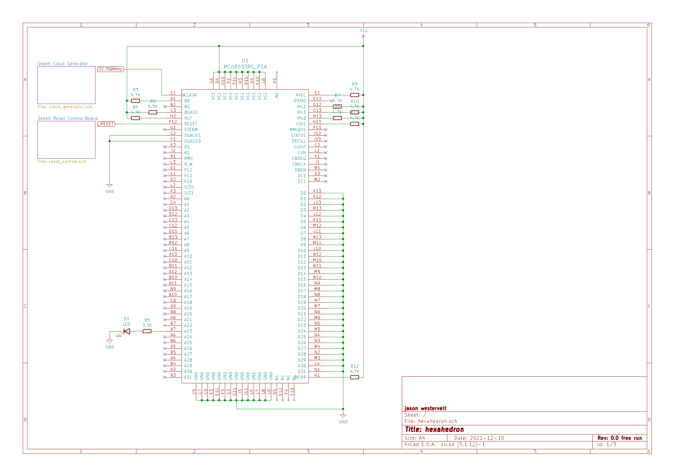
12/03/2021 at 01:37 • 0 commentsFree running was accomplished today and the CPU verified as functional on a 25MHz crystal.
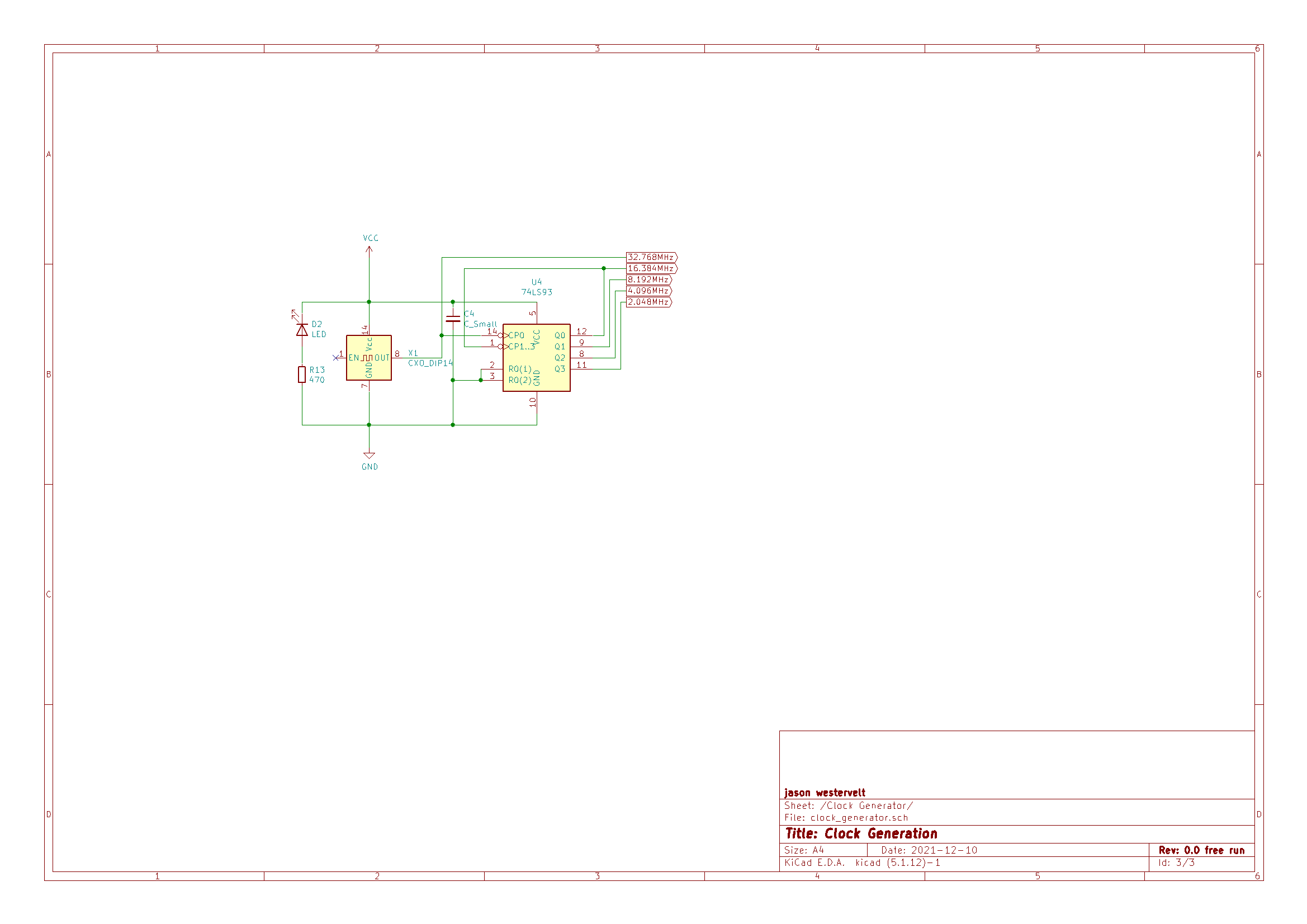
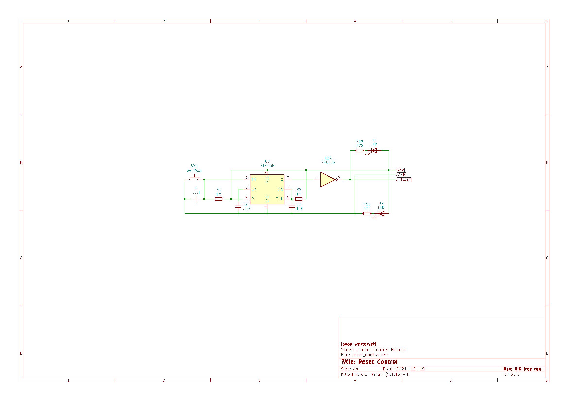
Photo in gallery with my oscilloscope shows the waveform on A21, whereas the LED in the video is attached to A23. A21 (bit 22) is cycling at 5.95Hz according to the oscilloscope. 5.95 * 2^22 = 24.956MHz.Schematic below:
 Jason Westervelt