 James Newton
-
1Somehow find the chips
The problem is that now the versions of this chip you can buy on Aliberber or whatever are all fakes. Here's what I got last time I tried to buy them from "the usual suspects"
As far as I know, the original chip was designed by this company:
http://www.hhbytech.com/en/product-details.aspx?category=2&id=7
and I managed to buy them from yumin2191@163.com for years. I paid less than $10 each, but then had to pay a huge shipping fee to get DHL and import fees on top of that. I don't see ANY reliable sources for the chip.
If you decide to built it, for god sake, try to get it from the original MFGR. -
2Follow the steps from the site
http://www.massmind.org/Techref/io/stepper/THB6064/index.htm#Assembly
1. [ ] Surface mount Resistors. There are only two surface mount devices on this board, unless you count the driver chip as SMT because of the way it's being mounted. The components are large compared to most SMD and they really are easy to solder. The only trick is that there are no holes to hold the components in place by the leads, so you need some way to keep them in place while you solder. Almost anything that has 3 or 4 corners and won't melt can be used. A metal box, a heat sink, an aluminum extrusion, … anything. Probably the best is made from vice grips and a screw driver tip. If you don't have vice grips, wrap a rubber band around the far end of the handle of a pair of pliers. Or just tape one side of the part down with clear tape!
Once the part is held down in position, touch the pad, next to the end of the part, solder, flow, off. Solder one side of each part, check position, solder the other side.
3. [ ] Variable Resistor: This is the drive current adjustment. It can be installed either way but being able to get in there to turn it is the trick. Make sure you will be able to get to it after installing the other components. Take care not to melt the case by letting each lead cool a bit after soldering. If you like, you can even bend the leads on the variable resistor and install it flat agasint the PCB, with the shaft up.
4. [ ] Logic power options: There are 3 ways to get logic power, please select one:
External logic power via the PMinMO header: Nothing needs to be done to the PCB, just supply 5 volts via pin 9 (with ground on pin 7 or 2,4,6,8,10). The PMinMO header can be connected to the 4Axis board, or directly to a PC parallel port cable. You can provide power on that PMinMO header from the 4 Axis board, a USB port, or your own 5+ regulated power source. On the version 1.3 board, with VM greater than 35 volts, this is the necessary option.
Logic power without fan via VM+ < 35 volts: The onboard 5 volt regulator can supply the small logic current required from VM+ up to about 35 volts^. This is NOT recommended for the full possible 50 volts the drive can accept; in that case, supply external logic power as above. In this configuration the fan connector will be VM+ so the fan has to be able to accept the drive voltage or have a separate supply. For this option, clip off part of a lead from the large capacitor to short the two pins of U2 furthest from the edge of the board (nearest the "ERR" silkscreen) as shown here: TODO: Picture. Keep in mind, you will be applying >9 volts to VM+ when testing logic power below.
FAN Power regulator (Option): To use the FAN connector on the PCB, you need to install the large TO-220 LM317HVT or AHVT. This can manage the up to 50 volt motor supply and produce 12 volts at a high enough amperage to run most CPU fans. ERRATTA: There is an error in the values populated on the version 1.3 board: R8 is 240 ohm and R9 is 680. This results in the output of the regulator being 5 volts, which will not provide enough headroom for the already polulated LM7805 regulator to generate logic power. R9 must be changed to 2K2 ohms.
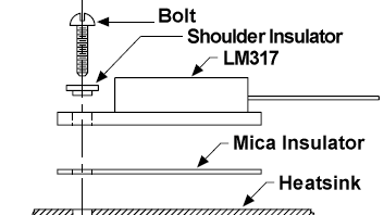
![]() If you do install the onboard logic power regulator option, the LM317 goes in U2, with the tab towards the outside of the PCB. The tab must be electrically isolated from ground, so a mica insulator must be installed between the tab and the heatsink, and a shoulder washer should be used to keep the mounting bolt from touching the hole in the tab. Keep in mind, you will be applying >16 volts to VM+ when testing logic power below.
If you do install the onboard logic power regulator option, the LM317 goes in U2, with the tab towards the outside of the PCB. The tab must be electrically isolated from ground, so a mica insulator must be installed between the tab and the heatsink, and a shoulder washer should be used to keep the mounting bolt from touching the hole in the tab. Keep in mind, you will be applying >16 volts to VM+ when testing logic power below.5. [ ] VRef Test Point: Form loops from a couple clipped leads and push both ends into the hole for the VREF test point just behind the motor power terminals.
6. [ ] Jumpers: When you solder on the 2x5 header for the options jumpers and the shrouded 2x5 PMinMO header, it's a good idea to bounce around in the pin order rather than just going down the line. It keeps the plastic from getting soft and perhaps not holding the pins straight. If you have the mating female connector handy, plug it in while soldering. Note the notch in the shrouded header is away from the edge of the board. Option 1 is away from the edge, next to the power cap. Option 5 is near the edge of the PCB.
7. [ ]
![]() Terminal Blocks: Slide two of the three terminal blocks together so that the rail and groove interlock.
Terminal Blocks: Slide two of the three terminal blocks together so that the rail and groove interlock.4. [ ] Capacitor: The large electrolytic cap goes in with the long lead in the square hole, and the stripe side towards the round hole. It can be installed all the way down on the PCB for physical stability. And it's probably best to set it aside and come back to it after you have done all the other components. Save the clipped off extra leads for use as jumpers in the logic power section.
Assembly time to this point is about 20 minutes.
-
3Preliminary Inspection and Test:
11. [ ] At this point, without the chip installed, do a visual inspection, preferably with a magnifying glass. If you want to be extra careful, you can check the resistances to ground at the pads where the main chip will be soldered on. Note: This table assume no option jumpers are in place. If they are, the DCY# and M# pins will be <0.2 instead of 12K. Pin 1 is on the left looking from the top with the chip away from you.
TOP:
Pin	Signal	Pad*	Normal 1	ALERT	1	OO
3 	DCY1	2	~15K or <0.5
5 	VREF	3	470-5K5
7 	M1	4	~15K or <0.5
9 	M3	5	~15K or <0.5
11	NFB	6	<0.5
13	PGNDB	7	<0.2
15	NFA	8	<0.5
17	PGNDA	9	<0.2
19	RESET	10	~15K
21	STEP	11	~15K
23	OSC2	12	47K
25	DOWN	13	6K2
VREF = ~470 to ~4K as the trim pot is turned Note: ~15K is 10-20K. VMA/B expect C1 dischanged
BOTTOM:
Pin	Signal	Pad*	Normal 2GND	SGND	1	<0.2
4 	DCY2	2	~15K or <0.5
6 	VMB	3	~3M5
8 	M2	4	~12K or <0.5
10	Out2B	5	10K
12	Out1B	6	10K
14	Out2A	7	10K
16	Out1A	8	10K
18	EN	9	~15K
20	VMA	10	~3M5
22	DIR	11	~15K
24	VDD	12	>5K
Normal readings are not exact. *Pad is the pad count on that side.
If using PMinMO header, apply 5V logic power at pin 9. Otherwise, apply motor power to VM+. Now the 5V logic power system can be checked, the +5v led should be on and the Vref can be measured and adjusted to a low value: 0.4-0.5V. Power off and prepare for finally assembly.
-
4Final Assembly:
12. [ ] The big THB6064AH chip: Since this product has a MOS structure, it is sensitive to electrostatic discharge. These ICs are highly sensitive to electrostatic discharge. When handling them, please be careful of electrostatic discharge, temperature and humidity conditions. Wear a grounding strap when touching the chip and work on an anti-static surface.
The IC fin is electrically connected to the rear of the chip. If current flows to the fin, the IC will malfunction. If there is any possibility of a voltage being generated between the IC GND and the fin, either ground the fin or insulate it. We recommend that you directly connect the IC to the heatsink, and ground the heatsink.
If consistent mounting hole locations are important to you, use a drilled heatsink or template plate for this last step. Drill and tap for M3 or #4-40
Mount the chip and PCB using 3 #4-40 or M3 screws. Temporarily mount the chip to the heatsink first. On a large heatsink, you should also mount the PCB with a spacer to raise it up a bit so it won't short out underneath. Spacer height can be about 0.1 inch or 3mm. You can use an M3 or #4-40 nut, a stack of washers, or cut off a bit of tubing like an old bic pen barrel. If the heatsink is smaller than the PCB, like our little CPU coolers, just mount the chip in the center of the heatsink and secure the PCB to the cabinet next to the heatsink.
Slide the PCB between the chip's pins, align it carefully, and screw it down. The wide point on the outer pins should be just at the edge of the PCB. Any farther in, and the pins will start to spread apart and not lie flat on the pads. Make sure all the pins are flat on the pads so the solder will flow nicely over the length of the pin and form a strong connection. Bend them carefully if needed. Solder one pin by placing the tip of the iron on the pad near the pin and let the solder flow around and under the pad. Check placement, alignment, and orientation and then solder down the rest of the pins. It's a good idea to bounce around and pause once in awhile to keep the heat from building up in the chip.
Now take the chip and the PCB off the heatsink, turn them over and solder the pins on the back side. Check the following resistances from the actual pin of the chip (not the PCB pad) and these test points:
- Between chip pin 5 and Vref solderpad: <0.1 Ohm
- Between chip pin 5 and 5v+: ~4K5 to ~2K3 as the trim pot is turned.
- Between chip pin 5 and GND: ~470 to ~4K as the trim pot is turned.
- Between chip pin 12 to B+, pin 10 to B-, pin 16 to A+, pin 14 to A-: <0.1 Ohm
Finally, reassemble with a bit of heatsink paste under the chip. That paste makes a huge difference in high temperature operation.
-
5Final Test / Power Up
13. [ ] Apply only the +5 volt power again, verify the power LED lights and nothing gets hot.
14. [ ] Power off, connect motor power (but don't turn it on!) and the motor. For help with sorting out the motor leads, see: Stepper Motor wiring
DECAY
J J Mode
4 5 20%
4   60%  5 40%    80%
MODE
J J J Mode
1 2 3 half
1 2   8th
1   3 10th
1     16th  2 3 20th  2   32nd    3 40th      64th
15. [ ] Set decay and mode by adding or removing jumpers. You might start with only 1 and 5 jumpered: 60% decay and 16th. Option 1 is away from the edge, next to the power cap. Option 5 is near the edge of the PCB. microstepping.
16. [ ] Verify the current control potentiometer is set all the way to the lowest setting. Apply logic power first, then motor power. The motor should lock, but not turn. Make sure the drive chip and motor are not heating. Carefully adjust the current setting to 30% of the motors rated capacity. Why only 30%? Because when the motor is not turning, the driver is in idle and as soon as it gets a step pulse, it's going to increase the drive power automatically. Please do NOT measure the current via the +VM or positive motor supply lead: Because this is a chopper driver, the current measured at the +VM line is much lower than the actual motor; as much as a quarter to a fifth the actual current; to set current limit, you must measure VRef voltage.
To calculate the correct VRef voltage (at speed): Io = Vref * 1/3 * 1/Rs Since Rs = 0.20 Ohms then Io = Vref * 1.667 (at speed) For example, when Vref = 2.4 volts, Io = 4 amps (max) and when Vref = 0.5 volts, Io = < 1 amp (minimum).
When at rest, the actual Vref for Io = 4 amps (max) will be 30% of 2.4 volts or 0.72 volts. So to set for maximum amperage, while the motors are at rest, adjust Vref to 0.72 volts. For Io = 1 amps (min), when at rest, Vref should be adjusted to 30% of 0.5 volts or 0.15 volts.
Start with the current you want in amps. Divide that by 1.667 to get the correct voltage for Vref when running. Then divide that by 3.333 to get the correct voltage for Vref when resting. Set Vref to that voltage when powered but resting (not stepping), by following these steps:
- Attach a voltmeter (or multimeter in DC volts or "V=" mode) with the positive lead to the Vref test point and negative lead on ground.
- Apply logic (+5) power (unless using the power regulators)
- Verify the current control potentiometer is set all the way to the lowest setting; the lowest voltage on Vref.
- Apply motor power. The motor should lock, but not turn. Make sure the drive chip and motor are not heating.
- Now turn the potentiometer until your meter reads the correct voltage for Vref when resting.
NORMAL VOLTAGES WITH MOTOR AND LOGIC / MOTOR POWER
Pin	Signal	Normal 24	VDD	5V (4.6 to 5.5)
6 / 20	VMB/VMA	12V to 50V
5	VREF 	0.2V to 2.4V 23	OSC	1.2V
19 	RESET	4.6V
![]() 17. [ ] Now connect the step and direction signals and spin the motor. These should be < 0.8V when low and > 2.0V when high. The Vref reading should increase to your desired amperage setting divided by 1.667 while the motor is in motion, and drop back down when you stop it. Let it work for at least 10 minutes to verify that nothing is overheating. Power off and try different decay settings for smoother operation.
17. [ ] Now connect the step and direction signals and spin the motor. These should be < 0.8V when low and > 2.0V when high. The Vref reading should increase to your desired amperage setting divided by 1.667 while the motor is in motion, and drop back down when you stop it. Let it work for at least 10 minutes to verify that nothing is overheating. Power off and try different decay settings for smoother operation.Note: En (Enable) needs to be high. If you are building the RAMPs adapter cable, please do NOT bridge the two pads on the bottom of the adapter PCB. Bridging these pads with solder will cause the enable signal from the RAMPs board to be fed into the driver. However, the polarity of that signal for our driver is the opposite of that for the standard Pololu boards. As a result, the motors will lock when not moving, and release, failing to move, when the RAMPs system tries to move them. The enable signal is not required on the THB6064AH driver because it is enabled by default, and automatically goes into a low power hold when not in motion. If you do wish to make use of the enable line, you will need to change the polarity in the firmware. E.g. For Marlin, change the X, Y, Z or E _ENABLE_ON from 0 to 1 in the Configuration.h file
THB6064AH-SMT Stepper Motor driver
A great little driver, destroyed by knock offs
 If you do install the
 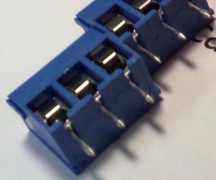 Terminal Blocks: Slide two of the three terminal blocks together so that the rail and groove interlock.
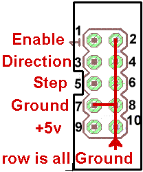 17. [ ] Now connect the step and direction signals and spin the motor. These should be < 0.8V when low and > 2.0V when high. The Vref reading should increase to your desired amperage setting divided by 1.667 while the motor is in motion, and drop back down when you stop it. Let it work for at least 10 minutes to verify that nothing is overheating. Power off and try different decay settings for smoother operation.
Discussions
Become a Hackaday.io Member
Create an account to leave a comment. Already have an account? Log In.