MKHBC-8-R2 - Multipurpose 8-bit Homebrew Microcomputer. Design and Specifications.
1. Architecture of the system.
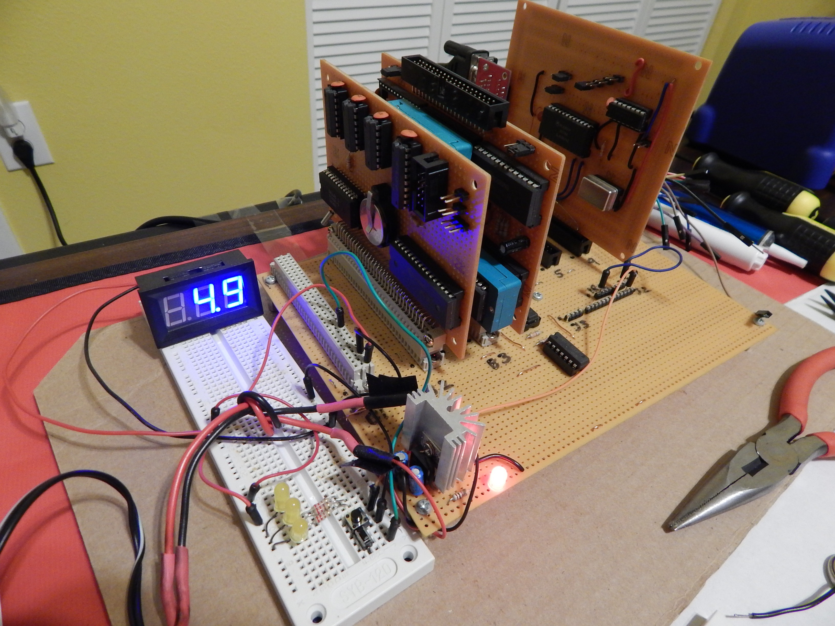
The system is intended as a hobbyist computing/microcontroller expandable platform. The CPU of choice is MOS 6502 compatible microprocessor. The design is a passive back-plane multiboard computer. It will consist of 2 buses:
- 3-slot CPU bus for CPU, RAM and graphics cards.
- Buffered 4-slot I/O expansion bus for other peripherals.
Other features:
- Programmable 8-input prioritized interrupt controller.
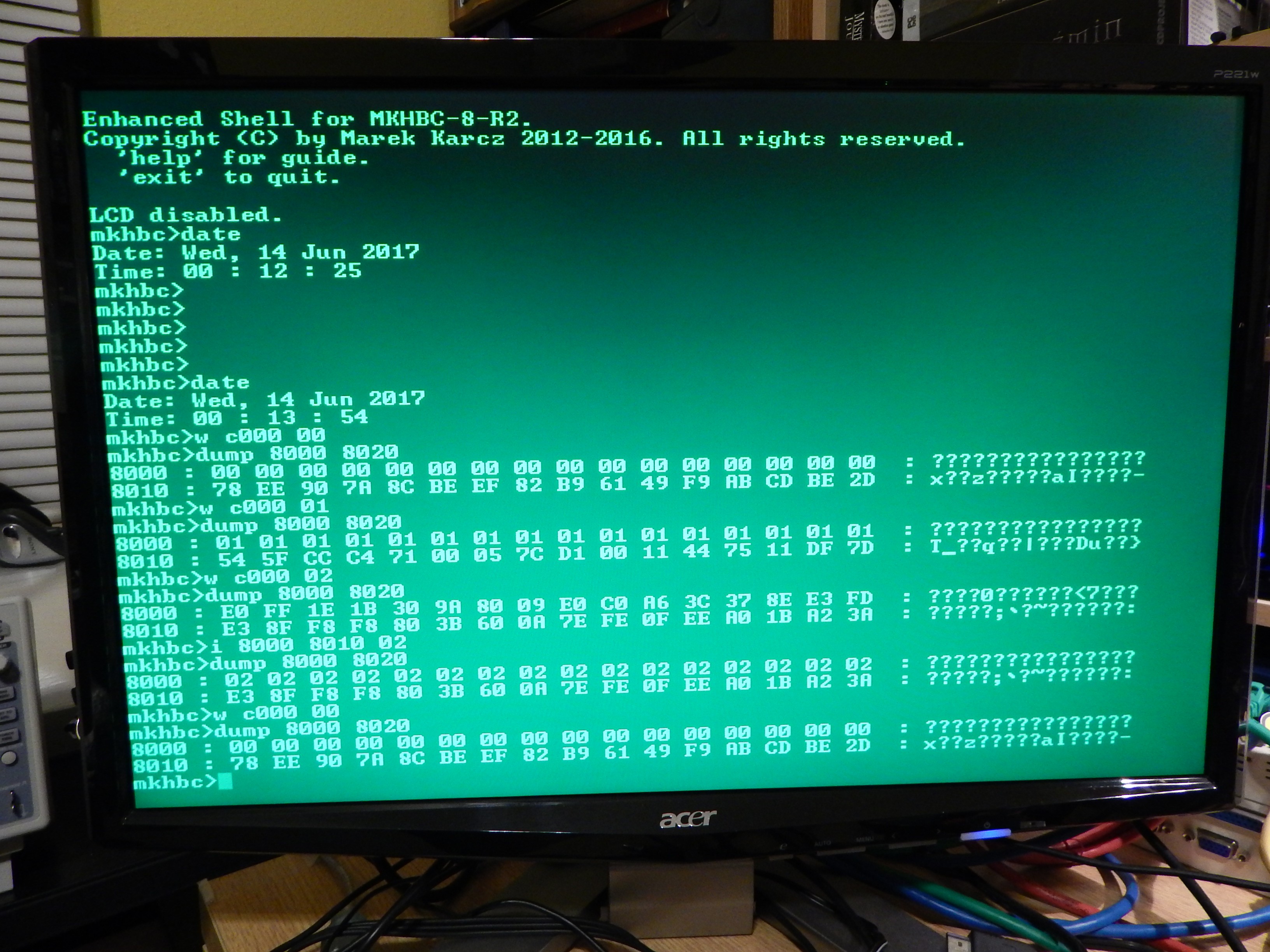
- Optional Real Time Clock with non-volatile battery backed SRAM for BIOS settings (DS1685).
- Optional banked RAM (128 kB: 16 kB x 8).
- Built in I/O port (6521/6821 PIA or 6522 VIA) for interfacing peripherals (joystick, I2C, SPI, serial keyboard, digital I/O).
- Control panel with built in reset key, NMI reset key, power switch and (connected to built in VIA I/O port): 16x2 LCD (or better) display, buzzer and 2 programmable keys.
1.1. Memory Map.
$0000 - $7FFF: Base RAM, 32 kB.
$6000 - $7FFF: Optional Video RAM, 8 kB.
$8000 - $BFFF: Banked RAM, 16 kB space x 8 banks = 128 kB.
$C000 - $C7FF: I/O space, 8 slots x 256 Bytes = 2 kB.
$C800 - $FFFF: EPROM, 14 kB.
2. Back plane/motherboard.
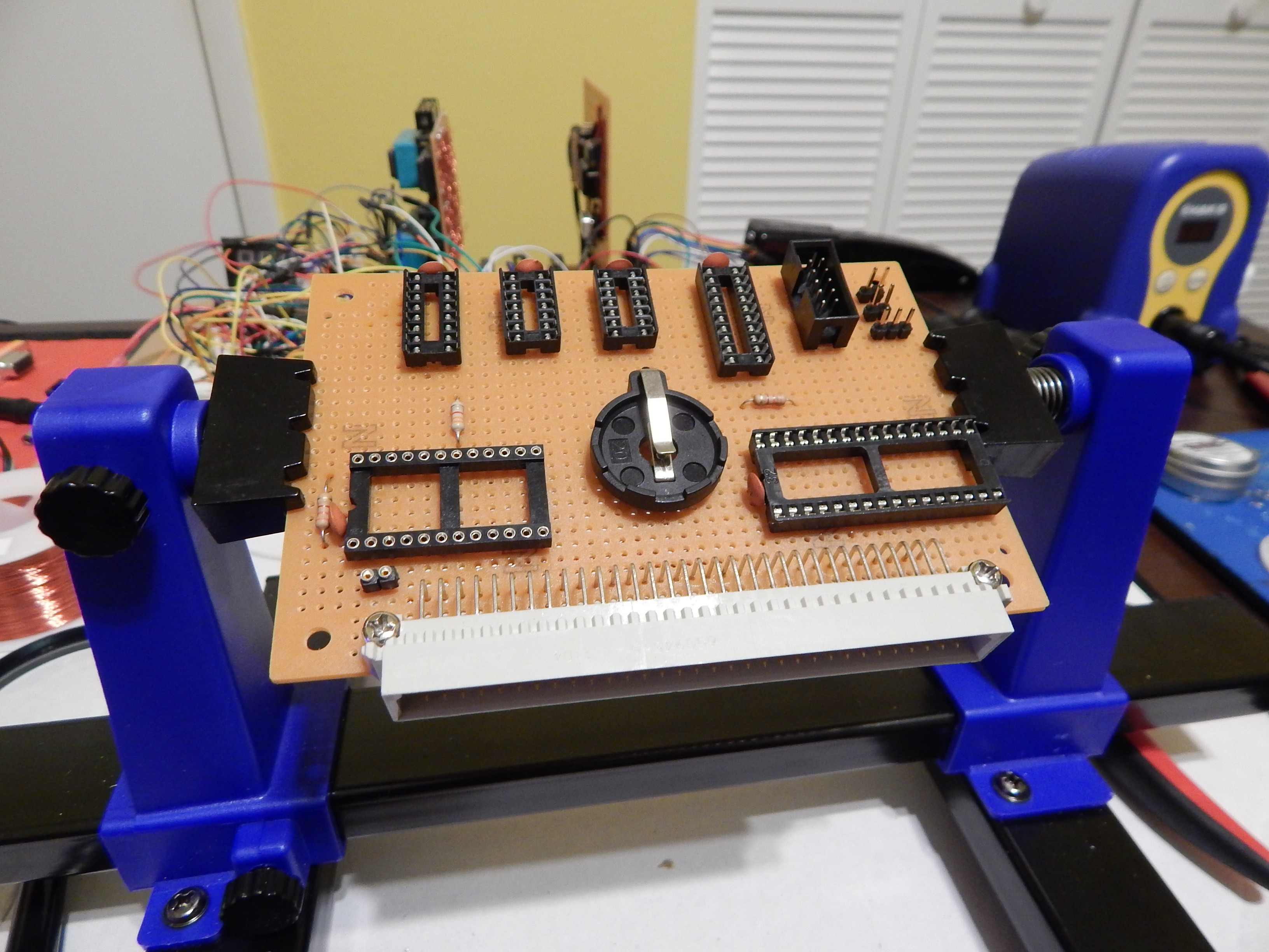
Motherboard will consist of CPU bus with 3 64-pin slots for primary components of the computer system.
The primary components will include:
- CPU card with EPROM, base RAM, reset/IRQ/NMI circuits and I/O address decoding circuits.
- Optional RAM expansion card.
- Optional RTC and battery backed SRAM card.
- Optional graphics controller card.
The I/O address decoding circuit will decode 8 I/O address spaces, from which 4 (slots 0-3) will be used for internal system's built-in I/O devices (RTC, memory bank switch register, interrupt controller, VIA I/O port) and the rest of the slots (4-7) will be used in expansion bus.
Planned allocation for internal I/O slots in mother-board mode of operation:
- Slot 0: RAM bank switching register.
- Slot 1: RTC and non-volatile (battery backed) SRAM for BIOS settings (DS1685). The RTC circuit with backup battery will be assembled on the same CPU-bus card as banked RAM.
- Slot 2: Prioritized Interrupt Controller. The circuit will be integrated on the motherboard, its control registers connected to the I/O bus.
- Slot 3: I/O. 6521 (MC6821) PIA or 6522 VIA compatible I/O chip. The I/O pins would be buffered and exported to the 40-pin connector. Using this connector, external devices could be connected to the system. E.g.: general purpose control panel (keypad, LCD, LED-s, joystick ports, I2C,/CAN/SPI ports etc.).
Planned allocation for internal I/O slots in SBC mode of operation:
- Slot 1: UART/RS-232.
- Slot 3: I/O (PIA or VIA).
Motherboard will also consist of fully buffered 4-slot 40-pin I/O expansion bus, which is intended for expansion cards designed by user. That bus will use I/O slots 4 through 7. The bus will allow to address 256 registers in each slot (8 address lines), will have full data bus and all CPU signals as well as derived from CPU supporting signals (/OE, /WE). Each expansion card can be a source of IRQ interrupt signal.
Planned I/O expansion cards (for slots 4-7):
- Mass storage controller (SD, flash, IDE).
- SID (Commodore) based sound card.
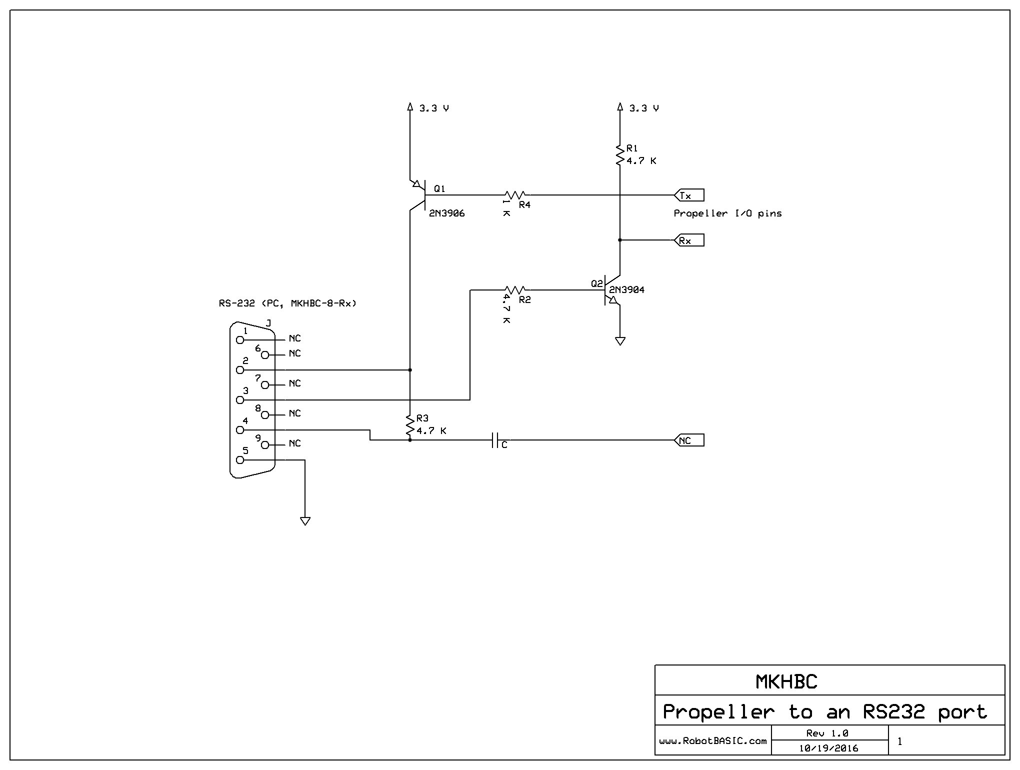
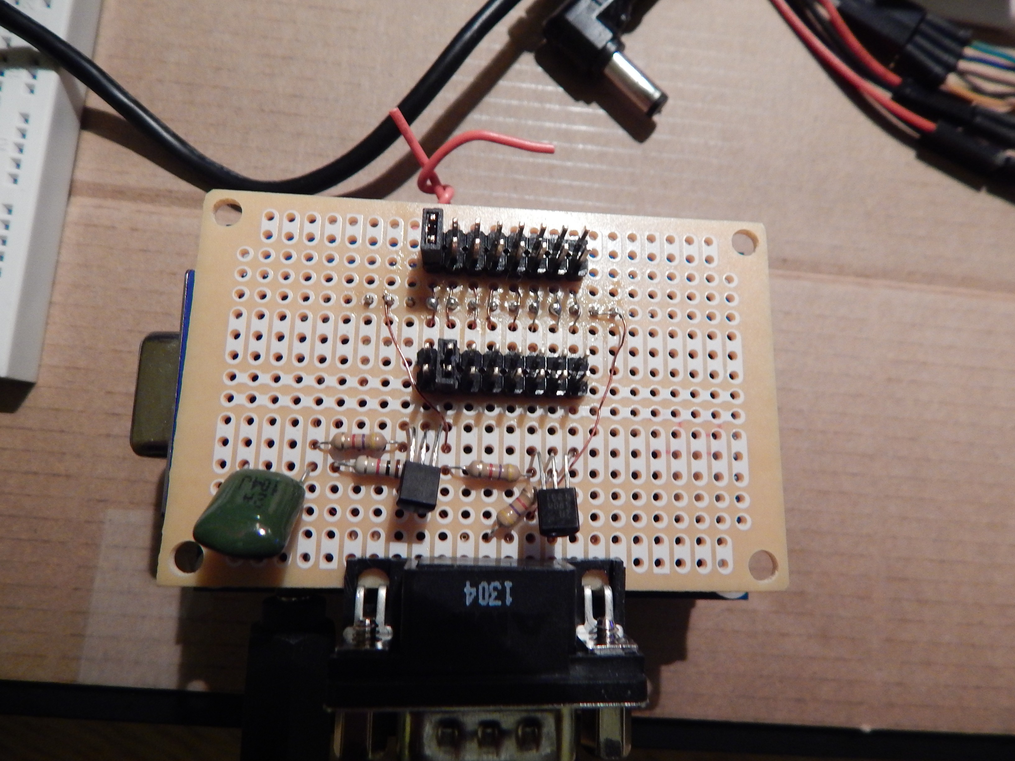
- UART/RS-232 (MC6850). - built
Planned CPU bus expansion cards:
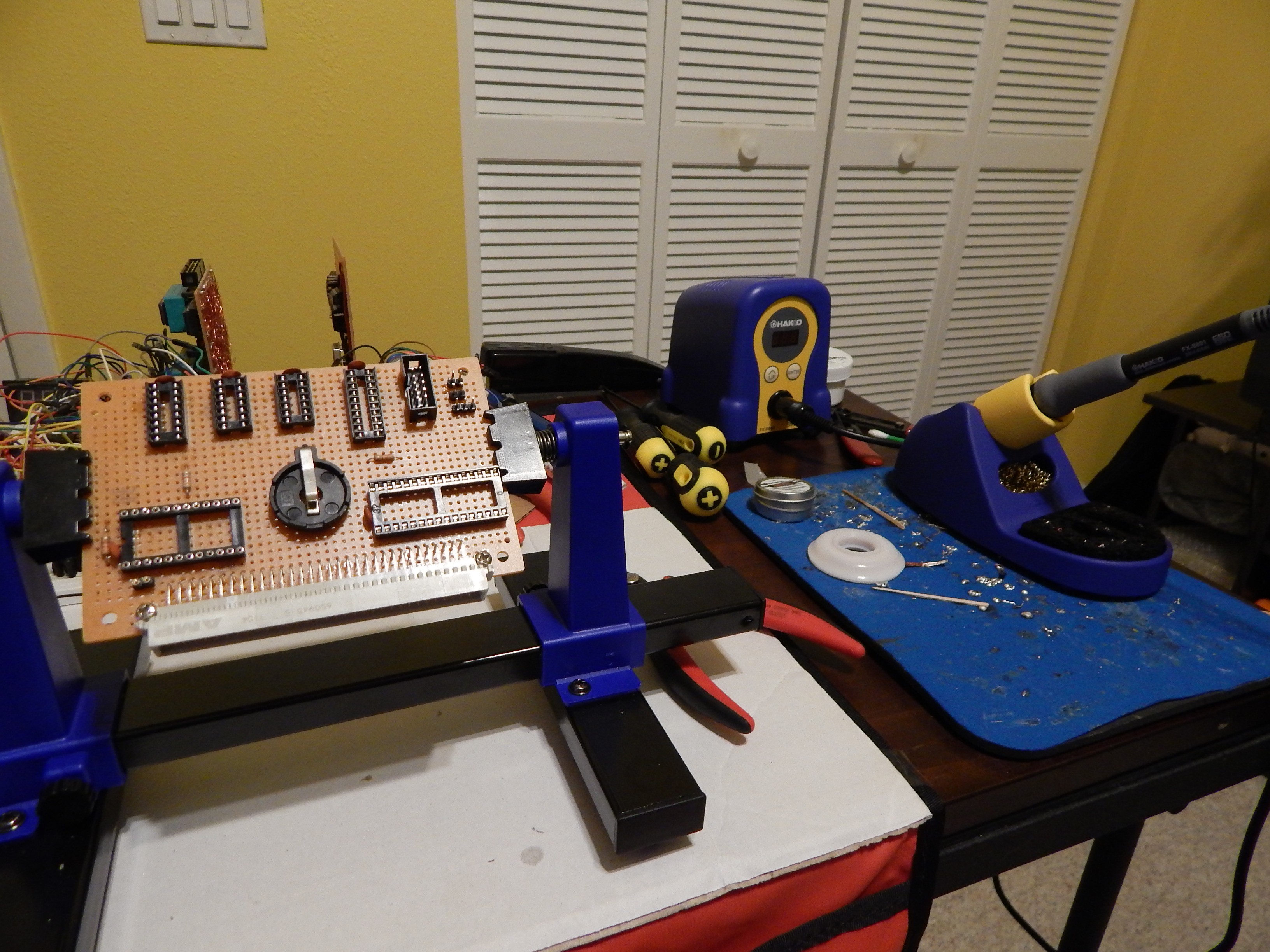
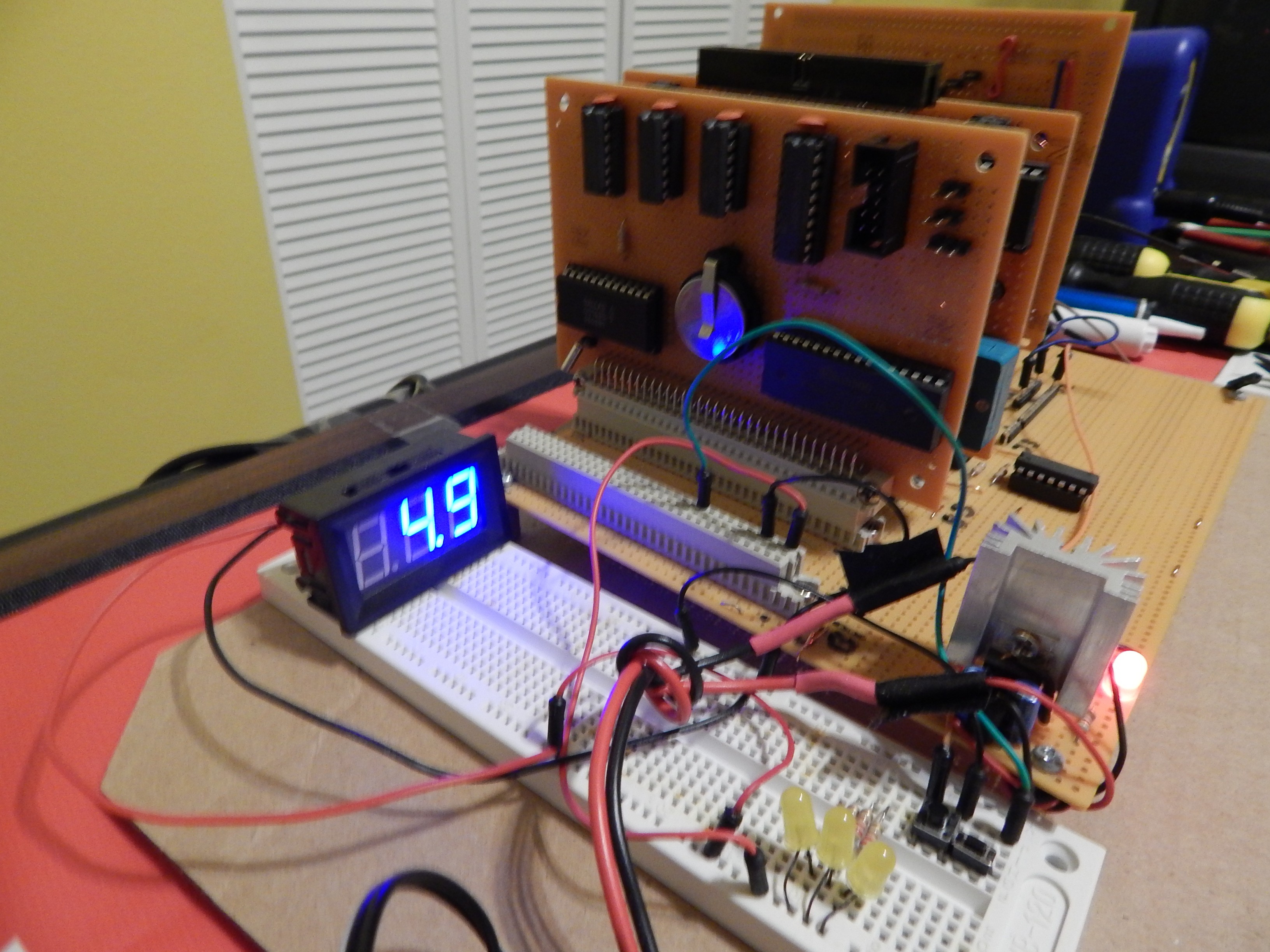
- Banked memory 128 kB + battery backed RTC and non-volatile SRAM. - built
- Video Adapter (MC6847 VDG - Video Display Generator, but also considering more contemporary PICASO board, VGA controller with serial port as command input/output).
User input:
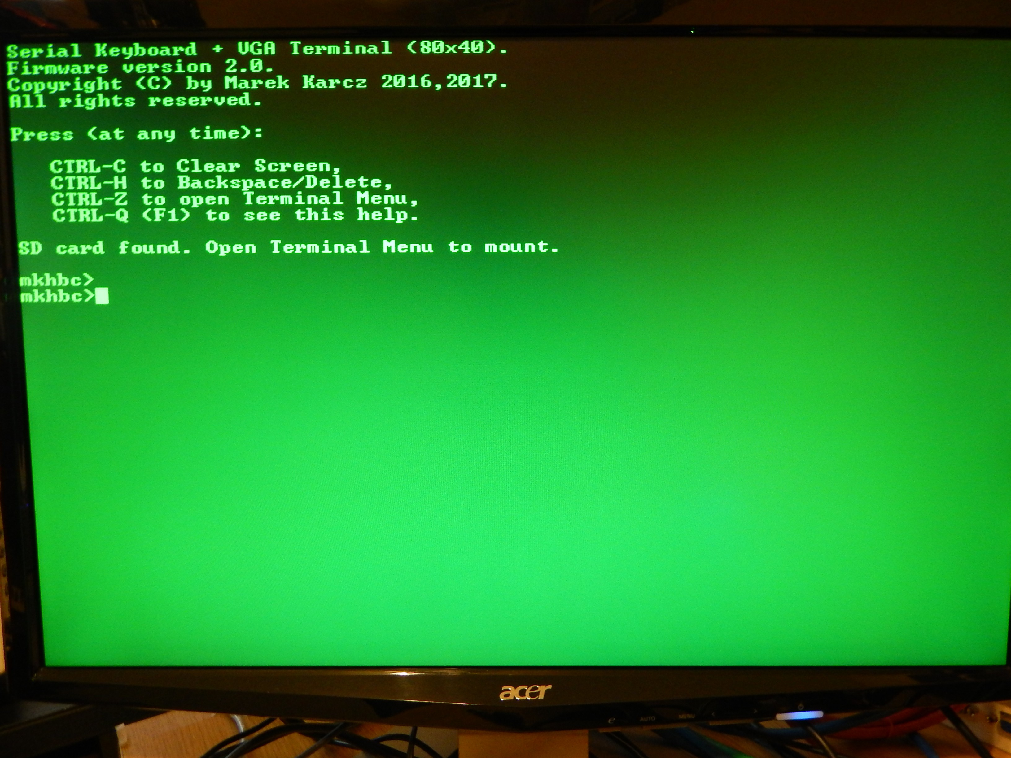
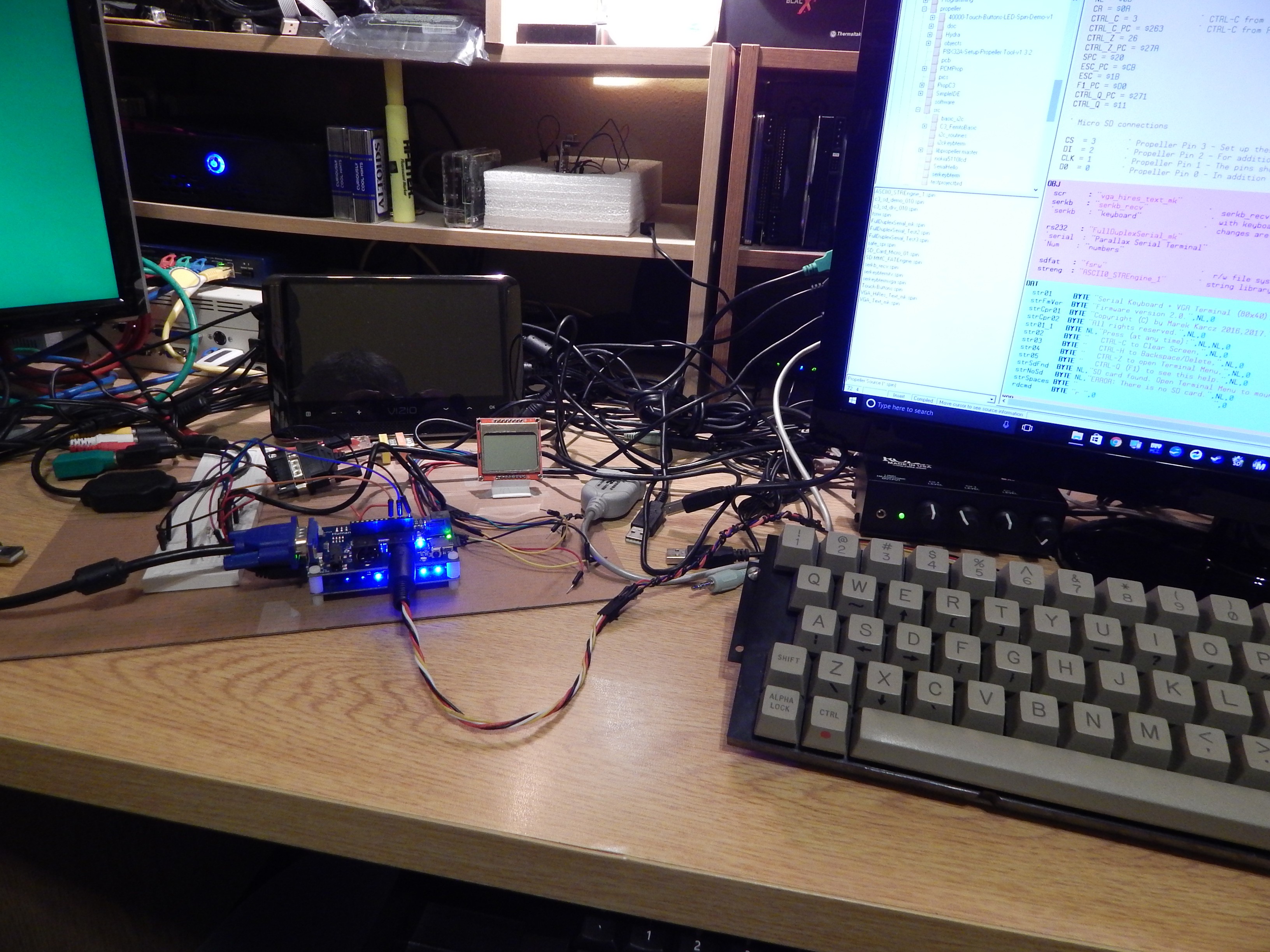
User input interface will be realized with full alphanumeric keyboard and digital joystick (C64, Nintendo, Atari compatible). The keyboard may be serial (UART, I2C) or classic matrix to be scanned in periodic interrupts generated by RTC chip DS1685 or timer in VIA adapter. If keyboard is to be serial, it must be the source of the IRQ interrupt which will read and store the input...
Read more »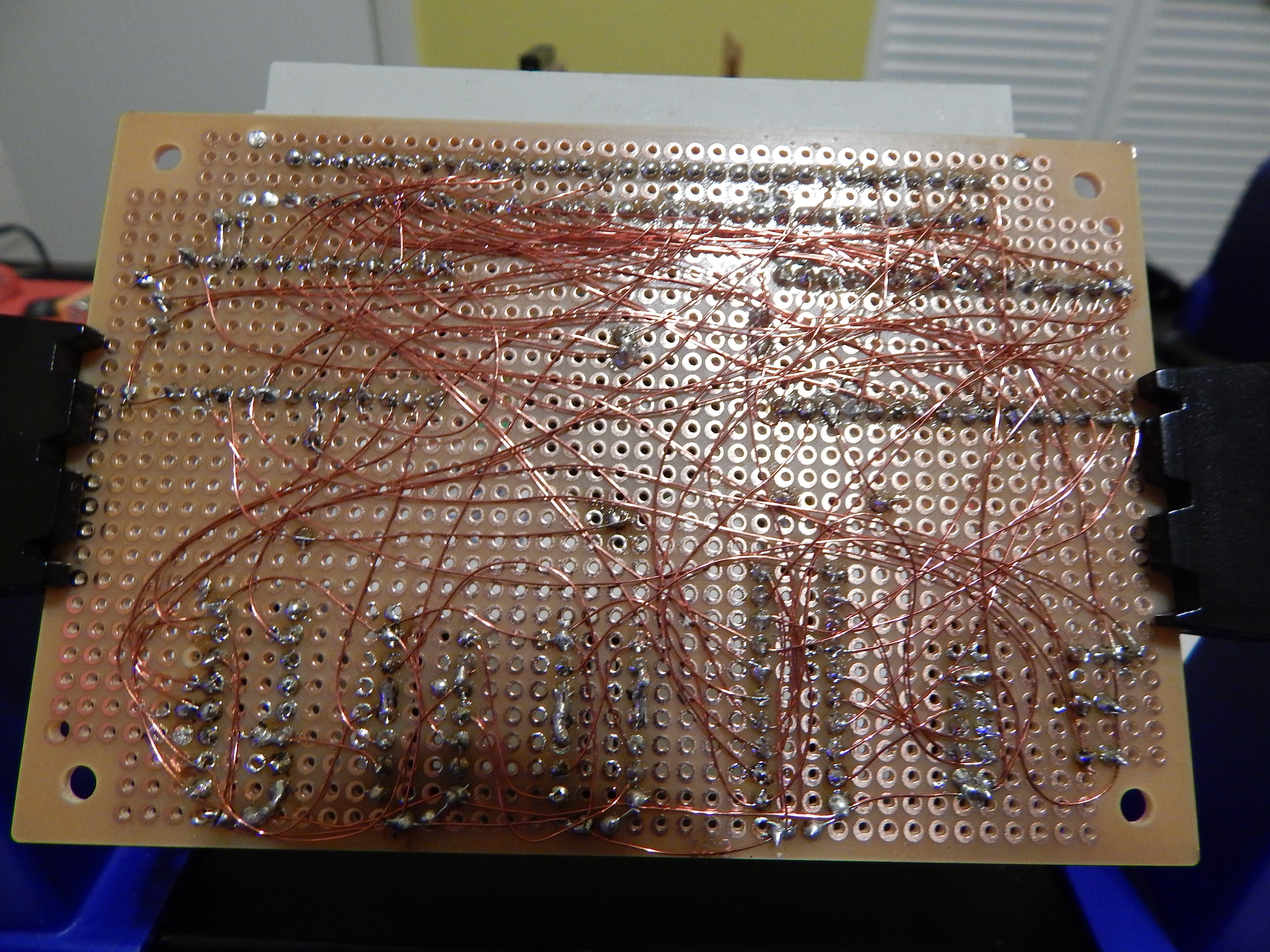



 Mars
Mars
 Jac Goudsmit
 Stuart
 Maarten Janssen
Nice Work!