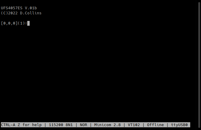
With my test program set up, test firmware for the micro-controller created. I settled in to test the ALU and register data path. I built a simple dumb terminal interface to control the whole project. (Firmware uploaded into the files section). The interface is written in C, this is later an issue but for now everything looks promising.
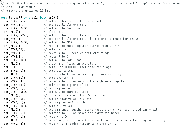
I set up the terminal to display the virtual stack pointer, and the two values to either side of the pointer (useful for viewing 16 bit numbers by centering on the big or little end.) I wrote a simple program to add 2 16 bit numbers together:
with out going to deeply into the C code:
cpu_ST() -- takes a value, and stores it into a register.
cpu_MV() -- moves data from one register to another
cnt_alu -- clocks the ALU
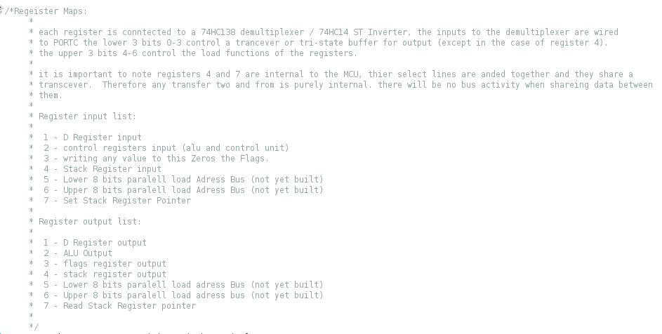
additionally for reference the register map:
The program simply does 16 bit unsigned math. It adds the lower ends together, then the higher ends, in between it captures the flags and uses an AND operation to simply remove the rest of the flags, leaving us with only the CO bit in the LSB position. When the operation is completed, then we add the CO flag to the big end. The ALU crunches the numbers:
and then the monitor looks at the registers and displays the values:
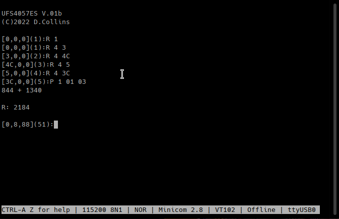
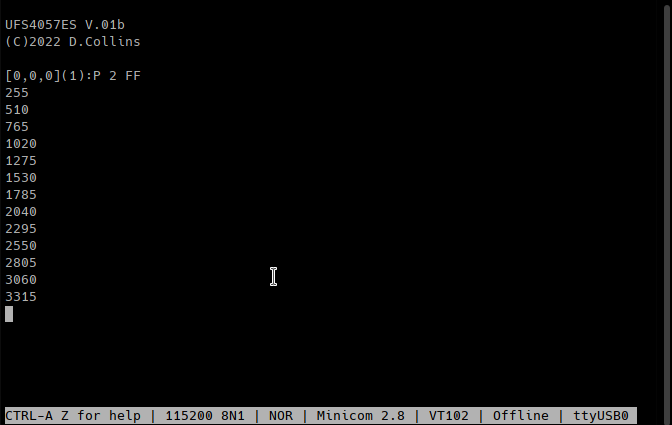
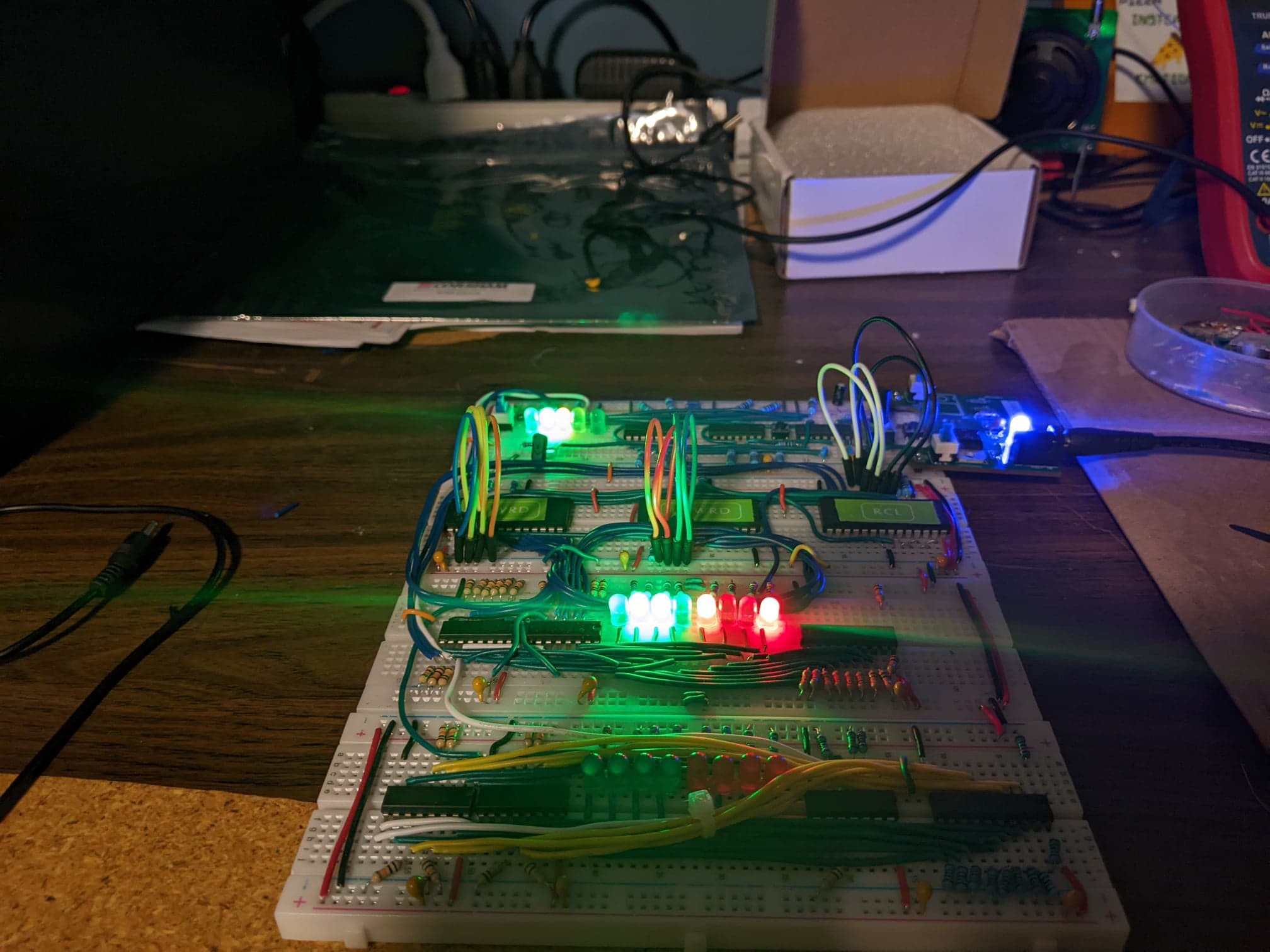
Above pictured, using the monitor to stage the stack (register 4 currently pointing at position 1) with the values, 844 and 1340. Next a command is sent to run test program 1, using stack positions 1, and 3 as the start of each of the 16 bit numbers (in this case big endian ). As you can see the internal register pointer is pointed at HL (51); showing the value 0x0888 after execution is complete. The serial monitor relays all of the numbers in decimal. Performing the conversion to decimal on the CPU this would require the control unit to be completely built, so in this case, the conversions are performed by the MCU. Additionally, there is a second program that simply performs this operation over and over:
The advantage to having a program that runs these calculations over and over is we can change the clock speed using the adjustable 500K resistor until corruption happens. I did these tests and came up with a clock frequency around .... wait for it.... 3Hz. Yes that's right, countless nights weeks and innumerable tiny jumpers, 3Hz.
I am elated.
Here's the thing. I set out on this stage to test the data path. I determined there are issues, that's a good thing. It means I did not get all the way through designing and building a control unit, that might only run at 1Hz ... in the best case (given that each micro coded instruction likely might have 1-3 steps.) So I'm glad now as this supplies me with several options:
I can optimize the ALU, and really take a look at the issues. Given the problem is related to the clock speed this is almost definitely related to the inductance in the board, or inefficiencies in the firmware.
I can shelve this project, seek incite of others to try to fix the issues with the build; work on other things, in the meanwhile.
I could take what I learned from this project, and start over building on what I have learned to make something else that works as it should.
I'm not disappointed, I feel really great having had the opportunity and the privilege to spend time tinkering with these things. But the conclusion I've come to, is that this ALU design is a case in making several key learning mistakes, many of them at the onset of the project. Feature creep hampers the design, several of the "bells and whistles" make the rest of the design less efficient. It has come from
This is the most common error of a smart engineer; to optimize something that should simply not exist. -- Elon Musk
I'd like to start over.
I think a new project with a slightly different ALU design.
Some of the limitations of my current design are:
The eeproms make things harder.
The eeproms have a very slow access time, compared to the logic chips.
The they need to be removed from the build to program them... I recently had to do that to make changes for left and right shifts, it was not trivial.
The breadboards are all different types. This causes a ton of issues with both capacitance, and inductance in the build.
The displays are unnecessary, take up space and might be causing noise inside the build.
when the build is running at speed there is no way to accurately use the led's to display anything.
they are time consuming to build, cut jumpers for and serve no purpose over a very low speeds
The ALU is based on the CD4057 this ALU has a in built register. The register in the bread board build is external but can not be loaded as an external register.
to load it, the control world has to be latched into the instruction register.
the D register has to be loaded with the data to be loaded.
the register can then be parallel loaded.
That's a lot to overcome simply by re-designing in my spare time. So I decided I need a break to re-evaluate this project. I would like to build a much simpler ALU perhaps 4 bits, most likely in CPLD or GAL. Id like the registers to be more useful, and dynamic. I would like the program storage and the program ram to be separate (Harvard architecture).
Whats next?
I am going to be doing a minimal 6809 build. I have a good reference design to start off with, I plan on adding more sophisticated decode logic; and a better clock circuit. I will most likely start on breadboards but the plan is to build something slightly bigger, and extendable like the RC2014 (except with a 6809). Ill do another Hackaday.io page for this project and do my regular (irregular lol) updates there and on minimalist computing on face book. Most likely in a few months ill look towards getting back into a custom CPU build, this project has been fun; but a chance of pace will be nice. thanks everybody who's provided feedback and support on this project, I really appreciate the kind words and support they truly keep me going and so for that, thank you.
Over the last month, life has been very busy. Between dealing with the things that go along with a family and kids and getting a much needed vacation in northern Wisconsin, there wasn't really much time for documenting what's been going on.
Here's a TLDR:
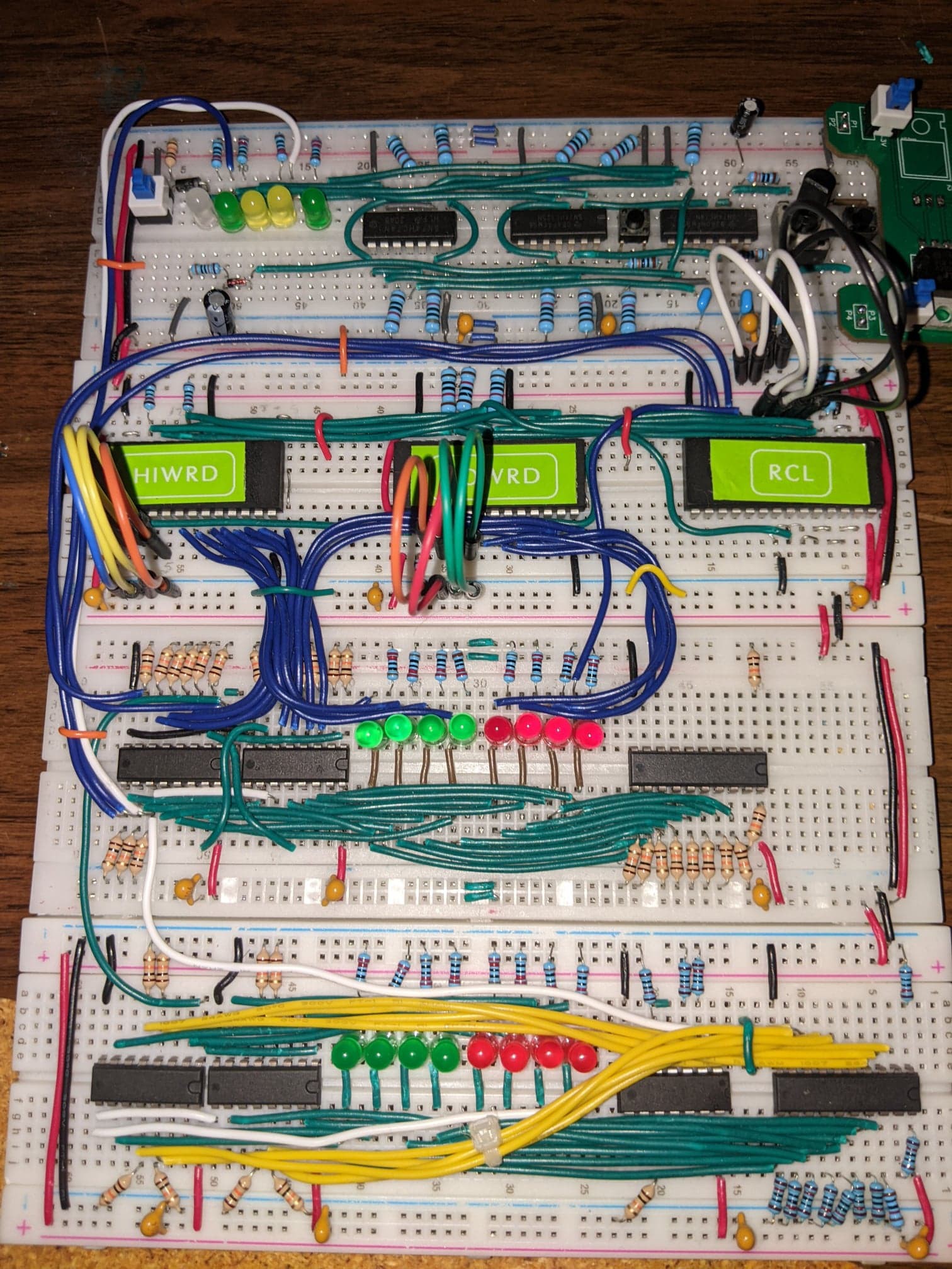
I added 2 MUX modules using a pair of 74HC138's which control the input and output of the registers; these each have a display of LED's and a 74HC14. (additionally 2 signals are displayed using a NAND as in inverter.
I added a flag's register that writes to the bus as register 3 on the mux, and has it's own reset signal that is XOR'd with the main reset signal when written two on 3 (any value). Having the XOR package then gave me 3 more XOR gates, I use in the place of traditional OR gates to glue some of the control lines together in situations where a single pulse on one or the other control lies is assured.
rebuilt the clock module, fixing very silly design mistakes, I also tightened up my reset circuit by using a 555 timer the main slow clock is still built on an inverter tree but the reality of trying to optimize something that should not exist reared it's ugly head so for simplicity sake I went with a very jelly bean 555 reset circuit using a spare inverter.
added some glue logic to fix some signaling issues brought on by using dissimilar outputs together on a common signal line (I know this is a bad Idea now... I figured it out the hard way).
added RS232 and a traditional serial port which is driven by the soft uart in the micro-controller
re-wrote some of the ALU logic to include a carry out bit on the flags register whenever a shift operation is going to overflow, this required removing and re-programming all three chips.
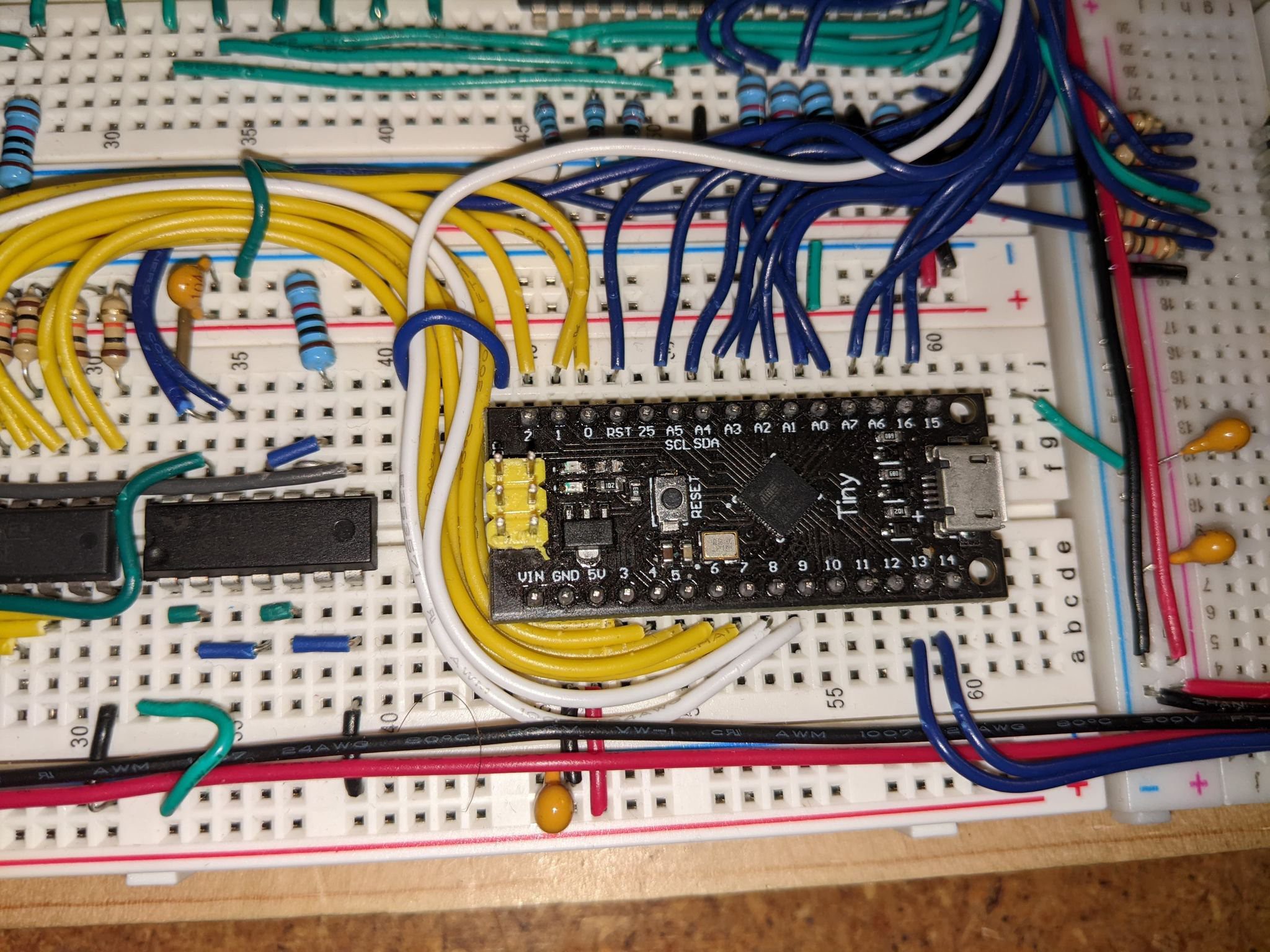
started and finished a "helper" ATTINY88 Micro-controller that acts as:
a very tiny stack
a soft uart
a few 16 bit static registers I think i will need
a machine language monitor.
this chip only provides these functions, and will not do any computation; aside from the stack pointer management (add and subtract 1)
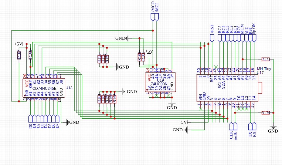
set up a bus transceiver and select logic to allow the micro-controller to read and write to the bus using its 8 bit wide port, and reside on the bus in tri-state when not active.
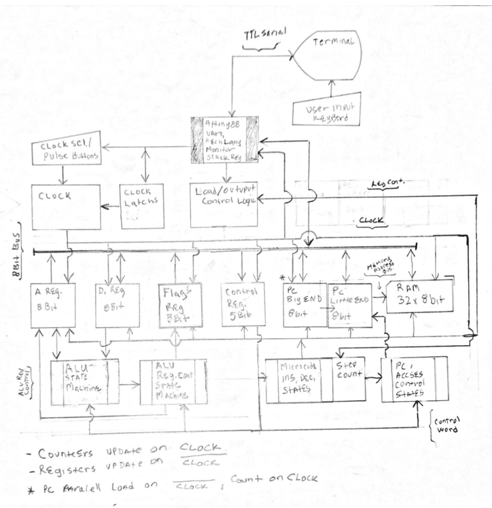
I drew up a vintage looking block diagram of what (generally) the finished CPU will look like.
This was all done in 1-2 hour spurts in my afternoons and during baby naps on my days off from work.
First off, Lets address the monkey in the room:
The attiny88, and what it is doing in a discrete logic CPU build. I thought this over a ton.... The ALU and its support registers + the control logic for the whole CPU is 8 modules (not counting the two side boards for serial and power.) The program counter, address bus management module, and the step counter module along with the state-machine(s) for the rest of the opcodes, not to mention the 32k of ram I am adding is most likely going to (I would like it to) fit on another 8 modules. I could add a discrete UART chip and a clock to control it but this is 2022. We have tiny micros that can be programmed for single task activities to do the same thing in much much less space. Why not use them? the way this micro is programmed it can not do anything save manage the UART, run the monitor and load the registers and ram. The computation will still be done on the CPU itself. There's a little space left over in the micro so I added some register capabilities to shuffle some data around and make the serial interface far easier to use. All of these functions would require more complexity and considerably more time / energy / resources to build. When I set out to build something based off a old chip, I never made it a goal to keep the design language free from modern conveniences, and having a micro-controller to test the data-path at speed is worth wile to me, and so I keep it. So thats that, I guess if that "wreaks" the design aesthetic for you, hopefully I can turn you around to my way of thinking via results later on.
The memory map of the internal "register space" for the MCU is:
Byte 0 - 00- Future use 8 byte static register
Bytes 1 - 50 - Stack space, when in this space the register behaves like a stack
example: if you set the stack counter to 1, and write to it 1 = the data, the stack counter will roll up to the next available space.
example: if you read from a byte in this range, the counter will decrement by one and the value in the space will zero out.
Bytes 51 - 52 - 16 bit HL register, behaves exactly like a static 16 byte register, and the pointer must be moved manually to access the register cell.
Bytes 53 - 54- Jump Register will be used by the microcode state, machine to store / reference the location of the next jump.
bytes 55 - 56- return register, this space is used by the microcode state machine to store / reference the return address.
bytes 57 - 59- UART values : 57 - outputs this value next write to terminal action, 58 - next available incoming ascii value or null, 59 - character ready = 1 if yes 0 if no.
This memory range is accessed by referencing register 4, and the stack pointer is read and referenced at register 7. The control unit may use some spare control lines on the MCU to quickly change the stack pointer before address bus reads and writes to make addressable jumps work better, but that has yet to be decided. As it stands I have 4 unused GPIO's on the MCU so there is room to add features if needed.
Additionally the MH-ET dev boards that I am using have a 6 pin ISP port for programming, and powering the build for quick testing. These little things though a bit dated, and sporting a practically useless micro-USB port due to basically non-existent modern OS Driver support, actually are supported by Arduino under Tiny Core. And can be programmed using a mini USB programmer like a USBTinyASP programmer. All of this means I can work on the firmware without popping the chip out to re-program it. This has made programming the firmware substantially easy, even more so than programming the EEPROMS for the ALU.
Clock and reset module enhancements:
The previous design for a reset line driver involving a Schmidt trigger inverter and an RC junction + a Zener diode for some sort of brownout / voltage drop detection, was basically for a lack of a better description poorly thought out. Though this worked through the onset there were massive issues with noise, bread board capacitance. If I had found the issues and done a better job sorting out the other problems with the build of the module Vs. the actual schematics I believe I would have had a much better time with it... but from the onset the Zener was never going to work as I had envisioned.
I wound up using the commonly used 555 timer arrangement in mono-stable mode, triggering the reset with an RC junction at the trigger pin of the timer. Then this signal is hooked to a inverter to buffer the reset line. As it has worked before for countless others (including the developers of the C64). This worked well in my build as well. However, I think if I build another CPU, or looking towards the CPLD version the design will designate / recommend a proper discrete reset circuit with a brownout detection there are many of these livable with / without a watchdog timer. I think that that is probably the best course to take.
The MUX modules:
I used the same inverter / mux arrangement that Ben Eater and others have in order to get 3 byte input / output. this gets combined onto a 6 bit control bus (with two lines left over from a full 8 bytes, one for the ALU enable signal, and another for future use). This allows the input and output of the registers to be controlled with a single port which is a nibble and a half. I used some of the spare space on the module boards for glue logic and the flags register.
The registers addressing are as follows:
Data bus register
Control register input / ALU output
Flags reset (on any write, flags are updated from the ALU), Flags output to bus
MCU D-Port (various internal memory ranges and registers)
Low byte address bus parallel load / read ( not built yet)
High byte address bus parallel load / read (not built yet)
Stack Pointer (managed by MCU)
The micro-controller has 4 ports, one of them has a nibble and a half exposed to the pins on the dev-board right in a row. this makes it perfectly accessible to use IO register manipulation to control the MUXes from within the bootstrap environment. This allows the micro-controller to take full control of the RAM (once built) and the control bus in order to load the ram, and kick off execution once the ram is staged with code.
The Glue logic / RS232 additions:
The simplest solution is often the correct course of action. As i am actually quite a novice to CMOS logic, I am learning as I go. One of the most recent hurdles I encountered was the effects dis-similar outputs can have on each other, when they share a data line. This is where Glue logic was essential to solving these issues. I amused incorrectly that an output is an output. (this is very far from the truth). Essentially I learned that trying to isolate outputs (with diodes or not at all) rarely works well. Unless all the outputs have some sort of tri-state cut off, you can't share a control line even if you try to isolate it with a diode. Doing so usually means an unwanted floating input at the very least, all the way up to wired oscillation / noise issues that can be very hard to troubleshoot. The solution in this case was simply to add glue logic where i need to control one input with two outputs. In most cases this was with an OR gate, since I needed a way to pass the /RES signal through to the flags register, and also provide a way of driving it low pragmatically, I used an exclusive or gate, so that when the register reset comes in from the inverter passed the input mux, the reset line for only the flags register is driven low. The remaining or operations are pretty much just assured "one or the other" signals, so there is zero likelihood that the XOR will drive low when both inputs are high.
I added RS232 support to simply isolate the RX & TX pins on the micro-controller from a direct connection to source voltages through the GPIO in reverse (which with this dev board ends up with half of a powered on state. This could be for a couple of reasons but i suspect that it has to do with how the GPIO pins are gated. Since the ATTINY88 does not support UART as native. Because of this I had to use a soft UART, which means that the RX/TX pins on the micro are just two GPIO pins which support a pin interrupt, (only a few on the ATTINY88 support pin interrupts but I picked 14 and 13. When linked with a MAX232, I simply get this isolation, and there is no path for the legs to source current backwards; so in this regard the problem is solved. Its also nice to be able to output a more normal serial signal, and I like the thought that even a very old terminal would have no problem loading code to this CPU.
ALU logic re-designs:
I added a few gates in logism (pictured is only the high word 1XXX rom, the low word 1XXX rom is slightly different to catch the LSB and carry out to the high word rom) to add carry out to the logical shift operations. The end result of this is we can now write code that will allow for shifts on binary numbers larger than 8 bits, without having to do extra store and XOR routines to come up with the bits manually. I think this will make the ALU more useful, and since the ALU only does single bit shifts, without this key component it would take massively longer to manually do this operation just using regular logic operations. In order to do this I had to make changes to each one of the truth tables for all three chips. TSV2HEX makes short work of the truth tables but pulling EEPROMs out of a fully populated breadboard was quite a task....
Whats next and conclusion:
I need to work on a test program that runs within the Arduino to test the ALU data path at the very least at 1kHz (the maximum clock frequency). At some point I'd like to build a 1-3MHz fast clock, I don't think this will get done until I have the test program up and working. I will do some simple arithmetic programs and something more complex such as generating prime numbers, or a psudorandom number generation using a user provided seed and a XOR and Shift algorithm.
I really appreciate the feedback I am getting on this project. I like to believe we are all learners and, this community (be it Facebook or hack a day), is a valuable resource for each of us to learn AND teach. Thanks for taking the time to check out my project. I usually have most of my updates on minimalist computing on Facebook, generally under the #UFS4057ES hashtag.
as always if im way off let me know, drop a line here or wherever else I am, have a wonderful week everyone!
Up till now, the design has been focused on devices solely supporting the ALU. We've talked extensively about the ALU and its inner workings and brushed a bit on the two registers which support it. Moving forward from this mid-point we start to look at parts of the computer that are external to the ALU. Having these systems in place will allow us to test the ALU, as well as support the rest of the CPU and computer system as a whole.
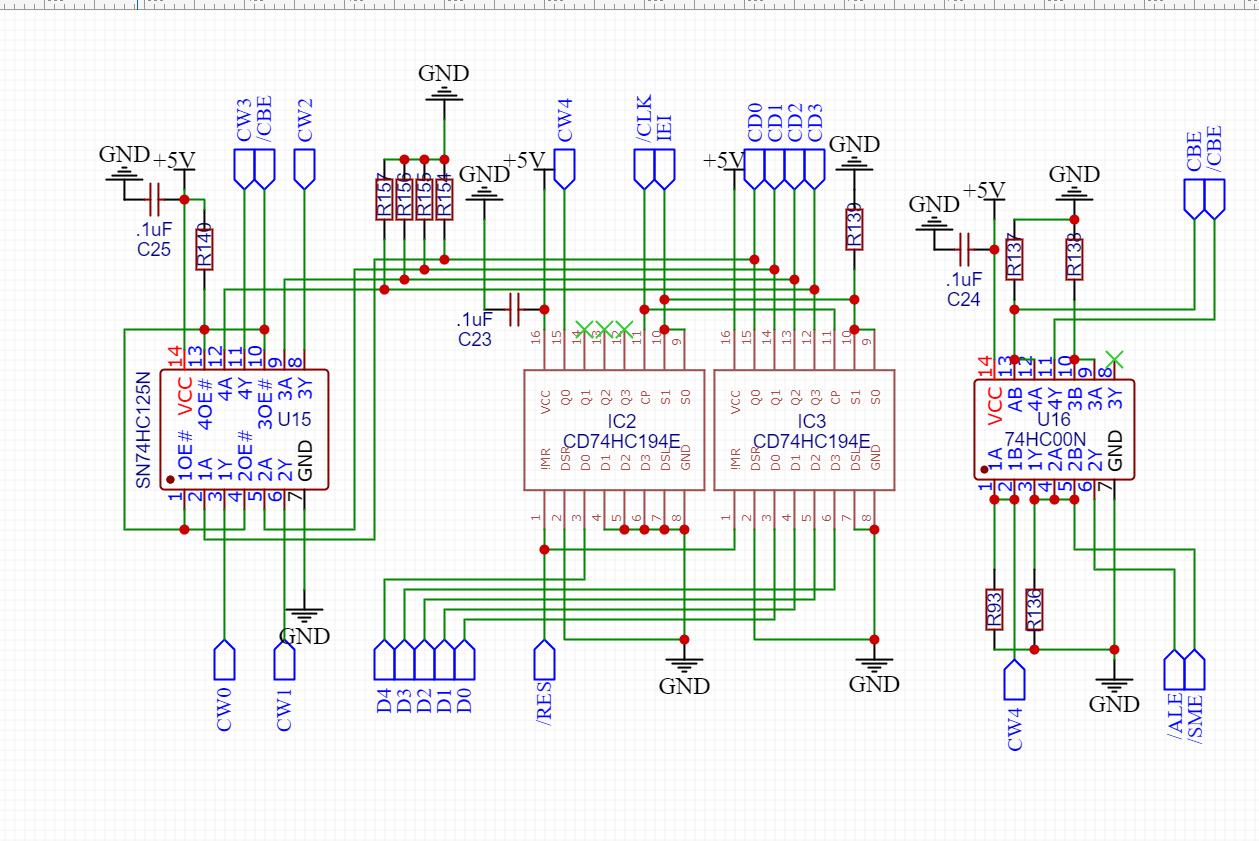
Instruction Register:
The Instruction register is 5 bits wide, and utilizes 2 74HC194E universal shift registers. I continue to use these registers because they have simple to breadboard inputs, and can be made into a simple parallel load register by simply connecting the the control inputs together. The instruction register outputs are tied to a LED display, as well as the control word inputs on the ALU (and eventually the microcode state machine instruction processor that will handle the other non-math functions.) The inputs are tied to the bus, and can be written to likely using a LOAD function from the instruction processor. An active high pulse from the input decode logic (controlled by the instruction processor, or the ATTINY88 ) enables the Load function on this register. The Most significant bit feeds a inverter tree, which switches the output enable on the ALU or the Instruction processor to determine which will act on the 4 bit instruction bus. This gives us 15 math instructions, and 15 general purpose register and memory functions. There are 3 bits left un-used in the High word register, which allows for some expansion if further instructions are needed we could use this to control other operations, but for now I've decided to leave it to just 30 instructions total. Lastly a 3rd inverter is used to control the instruction cut off, which is used to expose the instruction bus to the command word only during the write cycle(S) of the processor.
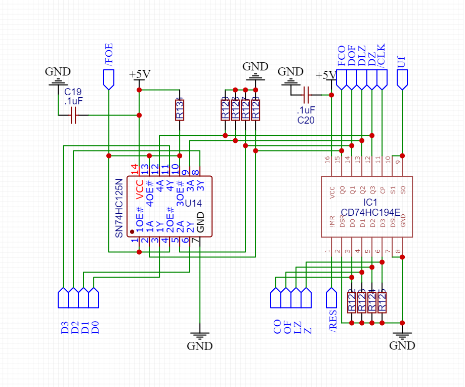
Flags / Output Decode Logic:
The Flags register records the ALU flags from the last mathematical operation. Its inputs and load instruction come from the register control and high word state machines in the ALU module. Each time a math operation is performed, on the falling edge of the clock, the register will update. The ALU determines weather or not the flags register will update the only time it is Zeroed out would be immediately after a reset; The reset signal of this register will likely be gated at some point in the future to allow it to be zeroed by the CPU, however for now, the programmer will have to clear the Zero state by setting a value in the accumulator using a math operation. The Flags register has it's outputs tied to the bus and can be read out onto the bus to be stored or used elsewhere.
The output decode logic uses a 74HC138N to select which register will output to the bus, an inverter is used to make the selection read out (for the LED's only ) make more sense. In this case the inverter is 100 % simply in place in order to make the Low signal which enables output elsewhere on the computer appear as a high signal (to make the LED's turn on ) when a register is selected. The control bus is a 6 bits (a nibble and a half). 3 lower bits control Register input, and 3 upper bits control Register output. these are connected to the rest of the system via the instruction processor or the attiny88. A third module is made that is basically wired identically to this which decodes the input control logic. As it is basically the same, I didn't feel the need to make a separate entry for taking a deeper look at it.
What is next:
So next up will be testing the ALU, this will be done using the ATTINY88. I opted for building in a modern microcontroller simply as a UART, and to bootstrap the memory. I don't have any grand plans for it beyond simply using it as a UART and a machine language monitor. Using the microcontroller i can simulate the rest of the build in order to find any issues through testing at speed, without actually laying in the parts needed to fully test the CPU. I have had some feedback questioning this decision, and I still think its a good idea because at the end of the day, to build in a UART I would need to manage a clock for timing; and with my adjustable rate design there's no way to do that without a separate clock. Since I have to have a separate clock and chip to enable a serial output I may as well have a programmable one.
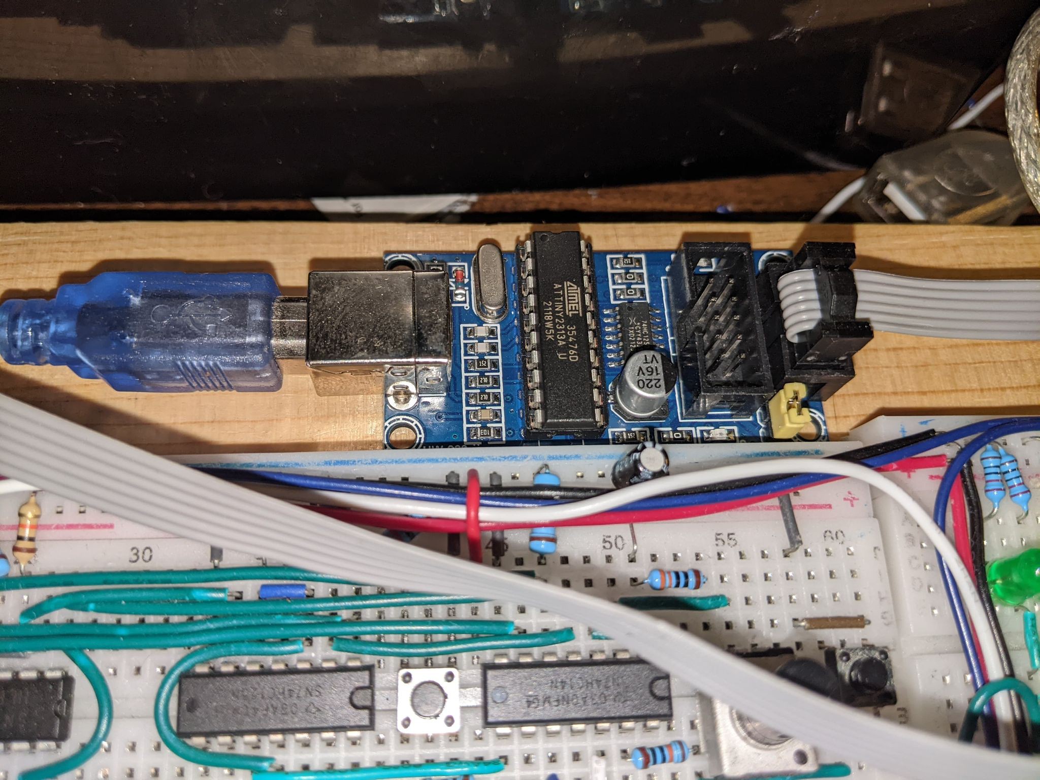
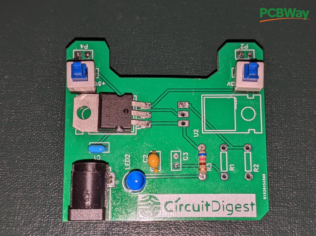
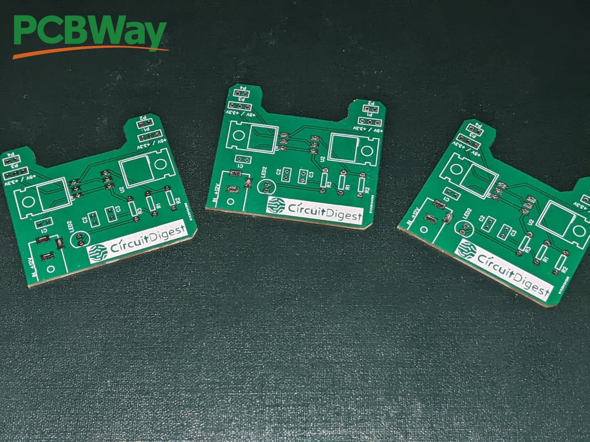
So for a while now I've wanted to build a small power supply for the ALU project. I really didn't want to spend a ton of time laying one out, and I didn't want to loose a ton of focus specifically working on the power supply because, I feel like I have a good clip on the ALU build. So stumbled across this project on CurcutDigest its simple; slightly sketchy, but it works.
About a week or two ago, this project started picking up some steam, and it found some notice with the folks over at PCBWay! They had offered to supply the PCB's if I would review their services. I've already used their services on some of my other projects, and have already been very happy before so I saw no issue putting this together for them.
First, the process was simple, just uploaded the Gerber files, clicked a few buttons selected a color and before I knew it the boards were on the way. It took about a week, using standard shipping the total cost with shipping came to about 20 dollars, for 5 boards, had I paid for them. Honestly for rapid turn PCB prototyping, the price is reasonable and competitive for the quality that you get. I've used a few different companies to have this done, and the quality PCBWay, for the cost, is hard to beat.
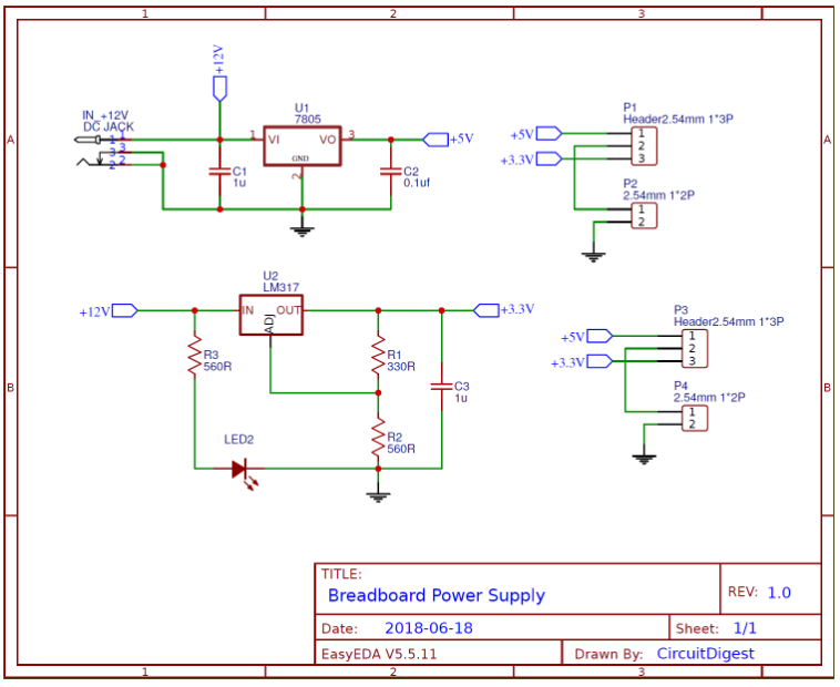
Lets talk about the CurcutDigest DIY Breadboard power supply:
The power supply is very simple, it uses a standard 8705 linear voltage regulator. and also has space for a LM317 Variable voltage regulator which can be configured for a second voltage, the design specifies values for a 3.3v regulated supply.
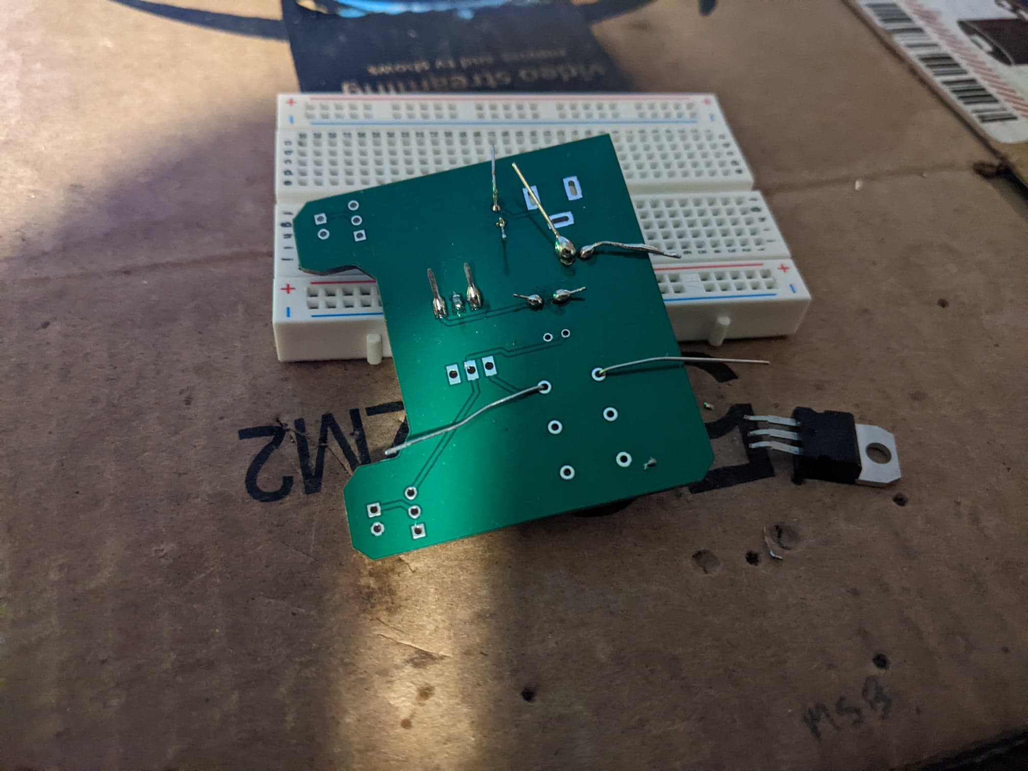
In my case I only built up the 5 volt side, and power LED. I also replaced the jumper blocks with 1 side of a few latching SPDT switches. The key to this configuration was making sure the switch covers the expected current for the circuit, in my case I think I am fine but it's something to watch if you want to try this mod. The nice part is you can use the latching switch to turn the power on and off from the board quickly without unplugging the supply from the wall.
Issues and complications:
When I built this supply Initially I had to start over on a new board because I tired to use a tip that was too small for the large ground planes, which cover both sides of the board; along with trying to use lead free solder that was still set up in my station. the results were not pretty:
I ran into some real issues with the very small modern through hole capacitor footprint, this resulted in some very poor soldering and i ended up damaging a regulator. I switched to a larger flat tip, with some 60/40 solder and everything went much better. The boards were also HASL finish, and I've had some issues with fine soldering trying to use mismatched solders like that, its 100% an error in judgement on my part, and not the blame of the board making process.
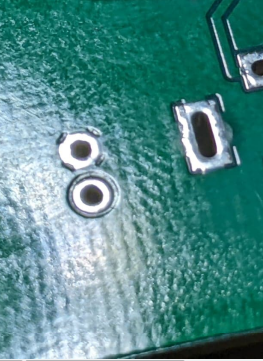
Another issue I ran into is:
The ground pin for the power LED, pictured here is towards the inside of the board
But as you can see, the silk screen is backwards. This is an issue with the PCB layout and not the manufacture, and another think to keep in mind if you build this board up, you have to install the LED in backwards, according to the silk screen.
Mechanically, the board could use another row of output bergstick pins, I think that would stabilize the connection to the board a bit better, with this set up I have to prop something under the supply so it doesn't fall off the end of the board. This might also be 100% my fault to begin with, as I have relatively cheep breadboards.
as you can see by the design, there is no heat sync on the regulator, and there's no protection diode, just simply the regulator and a few ceramic caps. Maybe at another time I can correct the schematics, and add some simple preventative measures for dead shorts and accidentally hooking up backwards, for now so I can move forward I'll be careful to unplug it, and make sure to check for major shorts before I add back power.
Performance:
It seems to work well, both toggles work to turn the power on and off though I should point out you should put both switches in the same way if you want them to function in the same way. This seems silly, but I'll be honest it's relatively easy to do and I had to de-solder and re install one of the switches after I had the whole board cleaned with IPA. The 5.032 volts I am getting out of this supply is better than the 4.8 I was getting from the USB cord with one end lopped off. The supply's designer says it has an upper limit of 1 Amp. I don't get any significant heat off the regulator with regular usage, I don't think i will get even close to that but the build is still quite young. All in all I am quite happy with this little side project. It went together in just about a week for a handful of parts I mostly already had, all told I don't think I would have spent more than 30 dollars on it, had PCBWay not kindly made the boards for me. Additionally I am left with a few spares, so I can make another if I need one without too much trouble. All in all I am very happy with the results.
Thank you PCBWay for your kind sponsorship of this power supply build!
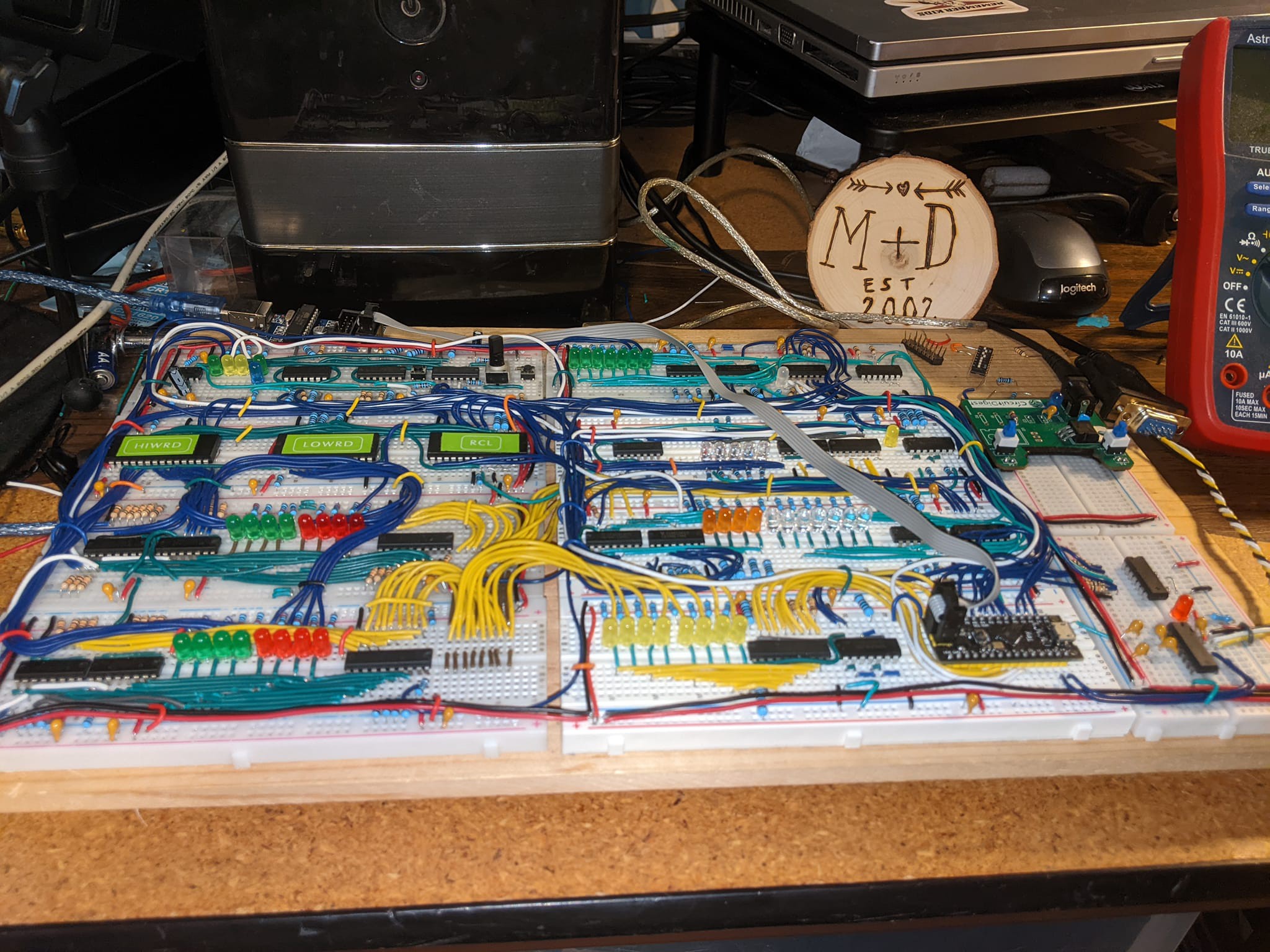
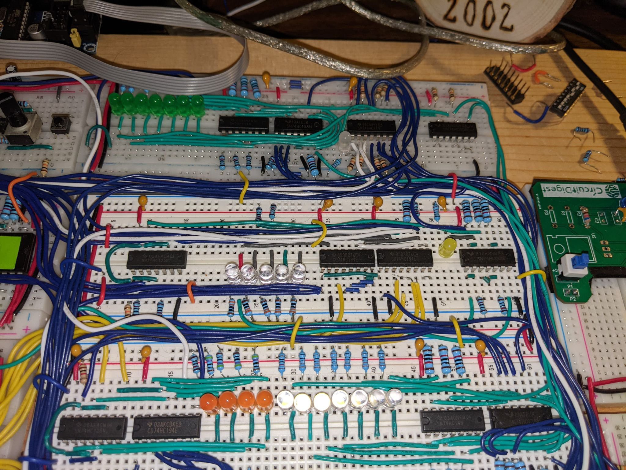
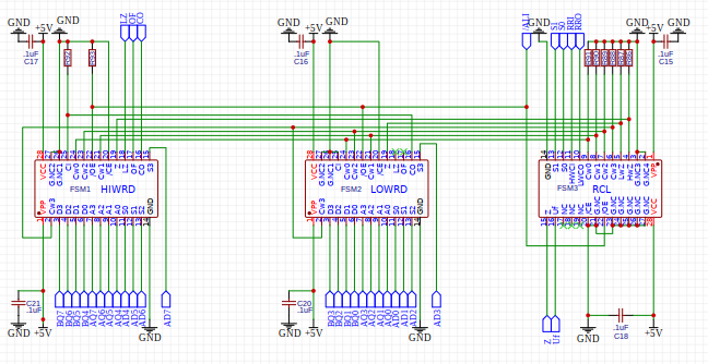
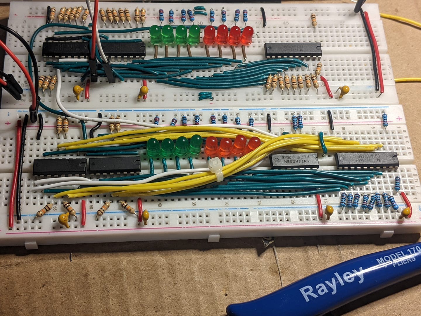
So This week I wanted to do a more in depth look at the ALU unit I have been building up. And since I didn't really get a chance to do a full deep dive post last weekend, This week there are two! In addition I have Partnered with PCBWay on a small power supply for the breadboard CPU which I'll be doing an exclusive build write up, PCB's designed over at CircutDigest. Its not my design but I needed something simple moving forward and I've been wanting to build something like this for a while now. PCBWay has kindly offered to cover the costs of prototyping for that project if ill do a small write up on my experience with their services, so if after you take a look at this why not head on over to my main project page, where you can find the write up on the power supply project. With that sorted, wanted to take some time to talk about the main attraction, the State Machine ALU.
Here it is pictured above. The module with the three EEPROMS is the state machine. The ALU's logic is 100% comprised of 32K eeproms (w27e257 specifically) :
These chips are inexpensive, available as pulls/used, and mostly available from the usual sources such as EBAY / Amazon (I've had good luck so far but your mileage may vary).
Using an EEPROM as a state machine is not new, but in these times finding parts for an actual PLA is getting interesting. In this case EEPROMS fit the bill nicely. Additionally I have a TL866 microchip programmer witch works out of the box at the 12v programming voltage these less desirable chips require.
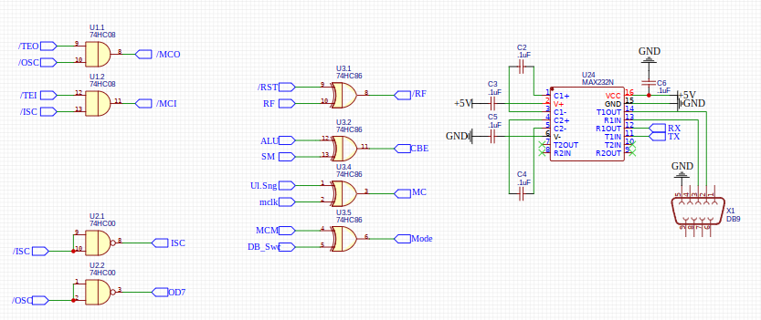
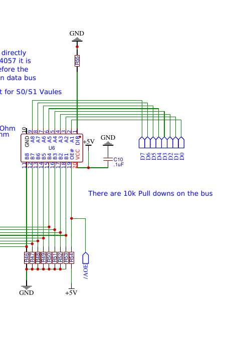
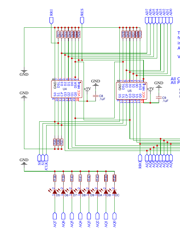
The Schematic for the ALU is fairly simple, I've re-labeled the inputs on the parts in EasyEDA to make the schematics more readable. The first two EEPROMS take care of the actual operations, while the third performs register and flag control. This absolutely could have been further simplified by using a 16 bit EEPROM for more states, but 32k EEPROMS are what I had on hand. When there's a chip shortage you kind of have to work with what you have. You'll note there's still two whole address lines unused on the main logic EEPROMS. Initially this was due to the 12 input limit Logism has for building a truth table, I later expanded it to 13 using some trickery in my tool chain to merge two truth tables together. the remaining two inputs are wasted, for the time being but could not really be efficiently used due to that limitation. That being said, I am planning on switching to Digital Logic simulator but I haven't tested this simulator to determine the limits for truth tables but this looks promising.
Each 4 bit unit is tied directly to the registers outputs before the bus transceiver. Its important to remember the EEPROMS always compare the registers regardless of the state of the clock (unless the EEPROM is placed in cut off by puling /ALI high.) The output writes directly to the input of the accumulator on the falling edge of the clock. This is of course a function of the universal shift registers which make up the accumulator module we've discussed elsewhere.
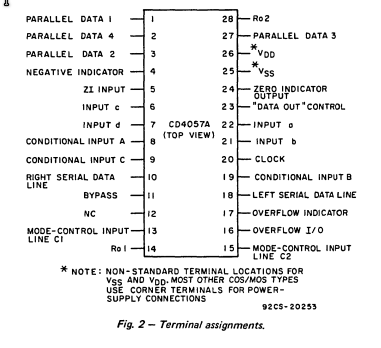
The two 4 bit units are different in a few ways and they all have to do with the arithmetic functions. Looking at the original COS-MOS part, we can see how the original compares to the state machine.
SOURCE: 1975 RCA COS-MOS Digital Circuits
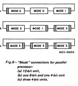
As you can see there are VDD/VSS pins on this and most COS-MOS parts, this was as i understand it (and somebody please correct me if I am wrong), in order to establish a high / low range for the part. The TTL/CMOS ROMS are only 5v but the original parts had a much wider input range. The indicator outputs are all covered under a more simplified single flags made on the main ROMS, and flag update signal made in the register control ROM. Zero is handled by all three ROMS with the two zero operations being checked by a logical AND in the register control, and output if both 4 bit units are actually zero. There is no serial bus connection, as simply the register is external to the EEPROMS. Instead, a more traditional carry in / out functions are used for both the arithmetic, and rotate functions. The clock is on the falling edge and is attached to the accumulator register module. The original part was intended to be connected to the parallel data bus directly. I had considered this initially, however, I came to the conclusion this might cause issues. We can assure the clock can never transition to a register update state at the same time the inputs are changing, if we simply assert both states with registers. Additionally the parallel bus was bi-directional on the original part, this instead uses bus-transceivers on the outputs of both registers. Doing it this way eliminates the need to share the d input and control bus, and eliminates the need for logic to control its function. This slightly increases the amount of time it takes to get data in place to compare, however the whole compare and update can happen with the rising edge changing the control word, and the falling edge updating the register, with an expected read, decode and write cycle of at least 3 clock cycles, the ability to compare two registers in a single clock cycle after being staged could increase program efficiency by a considerable amount. Lastly the conditional input lines define the word position or byte width, in our case we are using modes 1 and 2:
SOURCE: 1975 RCA COS-MOS Digital Circuits
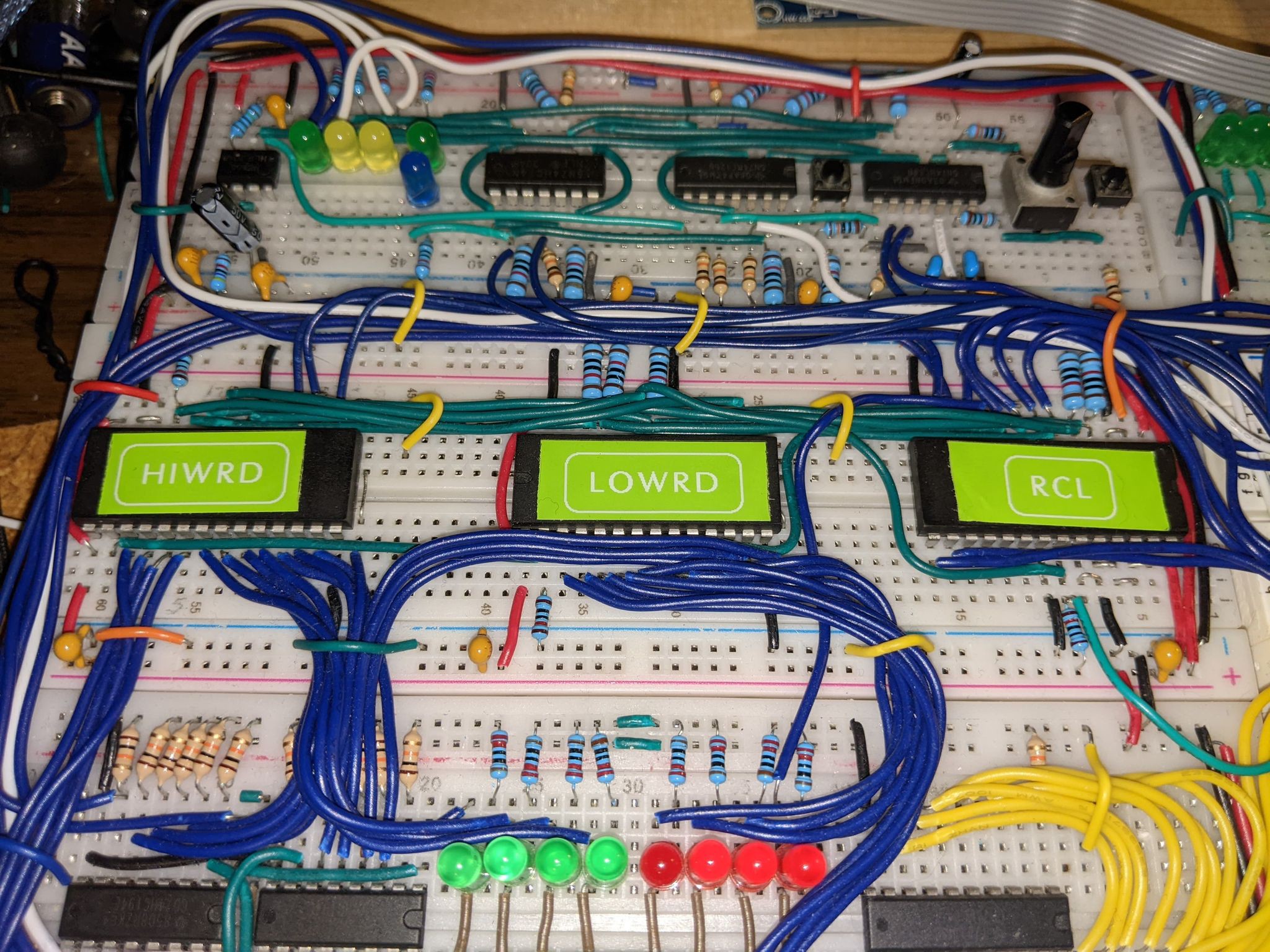
at some point with the two remaining address lines in the ROMS it may be possible to add modes 0 and 3, but for now were working with just 1 and 2. For our purposes MODE 1 is the LOWRD ROM, and MODE 2 is the HIWRD ROM.
MODE 1 AD (source: 1975 RCA COS-MOS Digital Circuits) - "adds the contents of the register to the data on the parallel-data lines and allows any resulting carry to leave on the left serial-data line. The right serial data line is open circuited. The overflow indicator does not change state. The CARRY IN is set to zero. In the case of our state machine, adds the contents of the accumulator to the data-storage. carry in is tied low via an external resistor, there is no serial data line, overflow will output but its open circuited."
In MODE 2 AD (source: 1975 RCA COS-MOS Digital Circuits) "adds the contents of the register to the data on the parallel data lines and the right serial data line. Any overflow sets the overflow indicator. The left serial data line is open circuited. The absence or presence of an overflow is registered. In the state machine, carry in is added to the contents of the accumulator, and the data-storage."
In the case of both Zero, Less than Zero, over flow and carry out are always calculated but flags are only read from the HIWRD and Register Control Logic (RCL) roms. The register control rom outputs a signal indicating when the flags should be updated (all four) this is on every non-rotation operation currently.
the count up control word simply adds a one, and ignores the data-storage. Following the exact same guidelines as the AD control word.
Subtraction is four separate control words, SM, SMZ, SUB, And Count Down:
In MODE 1 SM (source: 1975 RCA COS-MOS Digital Circuits) "same operation as AD except the contents of the register are two's complemented during addition in Mode 1 and Mode 3. In Mode 0 or Mode 2, the contents of the register are one's complemented and added to the data on the tight serial-data line and the parallel-data lines. Overflows occurring in Mode 1 or Mode 0 do not alter the overflow indicator. The presence or absence overflows is registered on the overflow indicator in Mode 2 or Mode 3."
SMZ subtracts the Stored Data from Zero, SUB Subtracts the Data Storage from the Stored Data, Count down subtracts one from the Stored Data. Flags operate identically to the addition operations within the state machine. And all of the subtraction functions follow the same compliment operations as the SM operation.
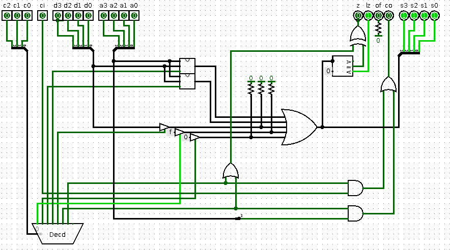
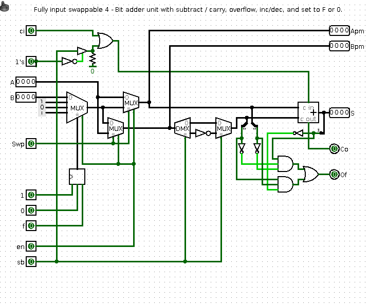
Above is a logical representation of the arithmetic unit. Larger operational functions were used as the goal was to create a truth table, not experiment with combination logic circuits. The basic idea is, this is a select-able 4 bit adder, with fully swap-able inputs, which outputs carry out and overflow. Subtraction is done by inverting the number to be subtracted and then adding it. Additionally you can sub in a constant operator (triggered by logic external to this diagram) for a 1 or 0, which is useful for CU, CD, and SMZ the logic for sending a operator of F ( all 1's) to the adder is also built but I never actually used it in the final design. Because the propagation delay is based solely on the EEPROM and not the internal logic I didn't have to worry about optimizing, since we only care about the resulting truth table.
As you can see the finite state machine has a ton of similarity to the original part, but lacks function and features that are just not possible with EEPROMS. I still consider it a huge hurdle to get a functioning unit at this point, even though it's not pin compatible. The propagation delays of the original part were quite slow, and while an EEPROM ALU is most assuredly not the fastest way to add two numbers, using semi-modern EEPROMS does afford far better than 1970s response time. Its very possible this ALU I've built even on the bread board could run at 3Mhz, and I doubt the industrial control applications that ran on this platform back in the day ever got that fast, its actually hard to tell since even the application notes don't state anything other than response time (in the realm of 100s of nS), and additionally much harder to find devices that were built using these chips. Since its an ALU there's no real concern to making an architecture that is compatible to run existing code, if there is anybody out there who's even got a clue as to what systems this may have been built in to shoot me a line. It would actually be fantastic to see what kinds of things that this chip was used in.
I've uploaded some new files: New logisim design, which includes a slightly updated register control. Additionally the files that correspond to that EEPROM and finally a new schematic including the ALU module and a quick and dirty layout and PCB for a regulated breadboard power supply, from Circuit Digest. I plan to do a full build and reflection entry as soon as I have PCB's at hand; this will include a video with a part by part soldering (if you like that sort of thing ). The PCB is very simple, Cheep and effective and its far and away better than my current hot wired USB cord and transformer set up. Hope to have some exciting news (well for me at least ) to go along with that next segment. By weeks end I should be cutting jumpers for the ALU, the rom's burnt perfectly so hopefully if the build goes fast I can do some actual tests with the accumulator.
I've completed building up both the data bus storage, and the accumulator registers. Both designs were developed to be very similar to the Ben Eater / SAP - 1 style register module. The two registers are slightly different, so I thought i'd try to explain my thought process here for each of them.
Bus Control
Each is separated from the main bus with a SN74HC245E bus transceiver; which is used to enable the register output.
A logic low signal is required by this package's output enable that will likely require an inverter to control the signal from the module handling the micro-coded instruction set; as its likely the EEPROM may have an issue driving the signal low, even with the weak pull-up. This will need to be a consideration for that module when I finally get around to building it. On the accumulator (pictured above) the data bus is only connected to the transceiver output, however on the storage register it is connected to both the transceiver output and the input of the d-latch which is used in that module. This was done, as the CD4057 has an internal shift register which can only be updated by the ALU via a control word; it is not directly wired to the bus. The Data storage register however is, and can be updated via the main bus or output its contents onto the bus. I've tied the direction in a fixed state B -> A, and tied the output by default to high Z, so that when the /AOE or /BOE signals are not present from the control module the register is in high Z. Additionally input enable signal on the storage register must also be enabled for the register to accept a clock tick, so when it is not enabled the register is effectively in tri-state.
Latch package types:
The latches for the registers themselves are either constructed from 74HC194E universal 4 bit shift registers, or 74HC175E quad D-Latches. The a pair of shift registers make up the accumulator:
This will require some decode logic on the part of the ALU to set S0 and S1 (which change the store or shift function of the register. Additionally, other logic will be required to detect and return a carry bit in the case of a rotation operation. currently this is built as an eeprom; but the logic is so simple I may switch to building this as discrete logic; or a low pin output high speed prom. The advantage to using a shift register is that it saves on states in the eeprom for handling the rotation and shifting functions, as well as drastically simplifying the truth table. The B register on the other hand, uses a pair of quad d-latches and an and gate:
An enable signal was added by a logical AND gate with the falling edge of the clock. This allows the register to simply drop the clock pules which are not significant to updating the latch allowing us to simply attach the main bus directly to the latch. This was necessary as the quad d-latch always outputs its stored value, and always updates on the rising edge of what ever clock pulse comes in. Lastly updates to this register will be through the system bus and configured by the control module.
Conclusion and what's next:
Now that the registers are set up, we are ready to move on to the actual ALU and a very rudimentary control logic. As always I've updated the complete schematics of what I'm working on, and those can be located in the files section of the hack a day page. For more updates, you can always watch this space or check out the myriad Facebook groups I frequent. Particularly Minimalist Computing, lately. I hope you all had a pleasant week, and I hope to update this space with more as more details reveal themselves.
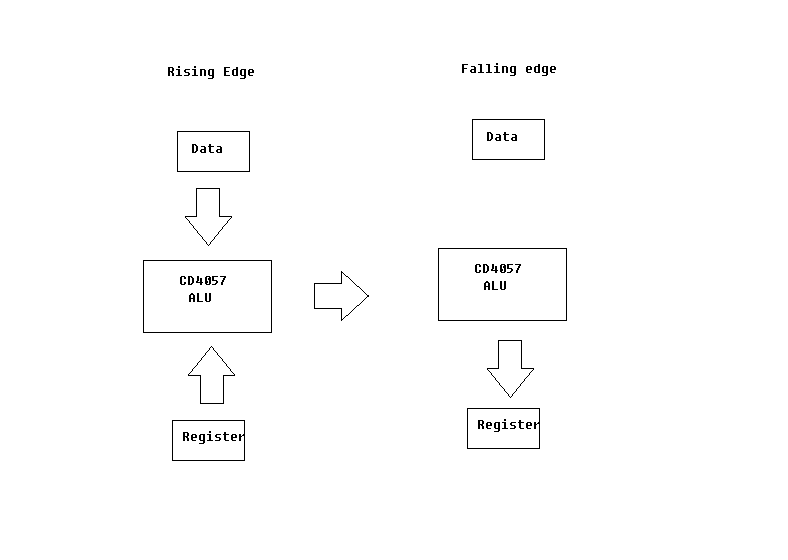
In the current project version of the clock module I wanted to have a clock module that had a fairly stable state, that had clean /CLK and CLK transitions (with no delay between the inverse and non-inverse state of the clock) both heaving a 50% duty cycle. Also, I needed to be able to half step through a clock cycle in order to see the data states at the high to low (and low to high transition). The main reason for this is the accumulator register is compared with the data bus on the rising edge in the ALU and clocked into the accumulator latch on the falling edge ( replacing the previous value from the latch, which was used by the ALU during the rising edge. )
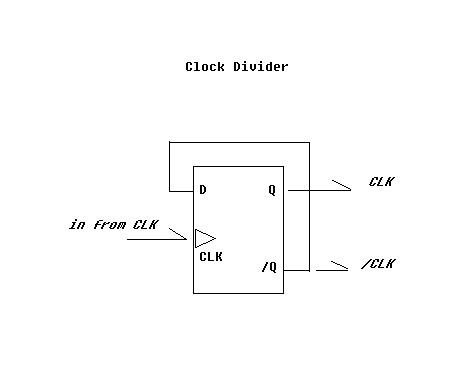
excuse the poorly drawn paint slide These transitions ideally will happen thousands or even millions of times in a second, and so it's important to have a clock that can properly supply carefully timed rising edges where we need them in order to facilitate these calculations without running into trouble. If we use a simple inverter on the clock from a 555 timer, when we being to run tests at faster speeds the propagation delay becomes significant. The solution is simple, generate both clock pulses simultaneously and eliminate the delay. We can do this many ways, using two parallel XOR gates, buffering the clock with similar parts , or as I've done use a clock divider and only focus on the rising edge of the clock. By latching the clock with a D-Latch, we assure a 50% cycle by only worrying about 1 thing, the rising edge of the incoming clock pulse. divide the unlatched clock and the outputs are 1/2 the input, as the state of Q flips on the rising edge of CLK
The incoming clock pulse can be at any duty cycle, and the resulting output will be based on the rising edge of the incoming clock pulse only. This has the advantage of generating a output that is exactly 50% of a duty cycle based on that rising edge, likewise the rising edge of /CLK is exactly at the same time as the falling edge of CLK. This has the glaring issue of reducing the incoming result from the oscillator by half, we can overcome this issue by building an oscillator that is twice as fast as we need.
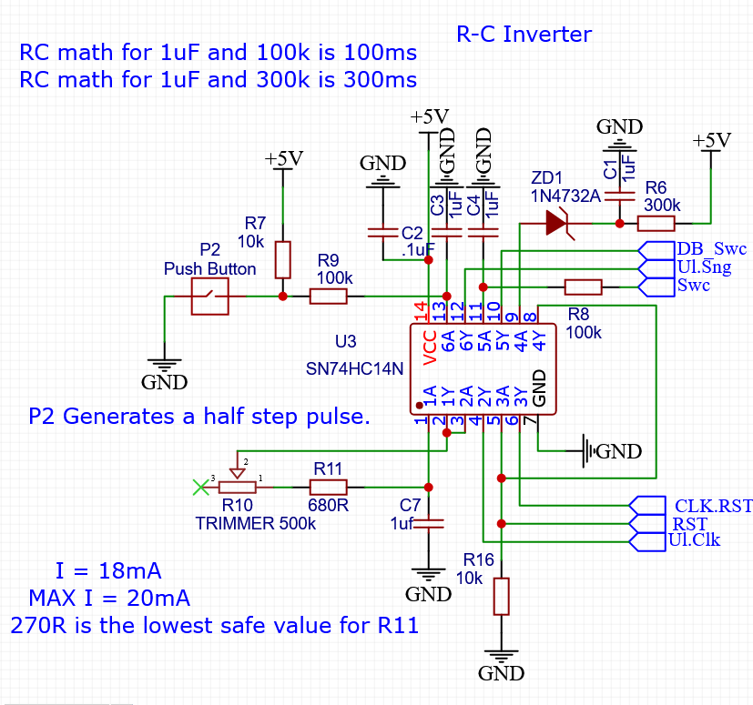
R-C inverter Circuit
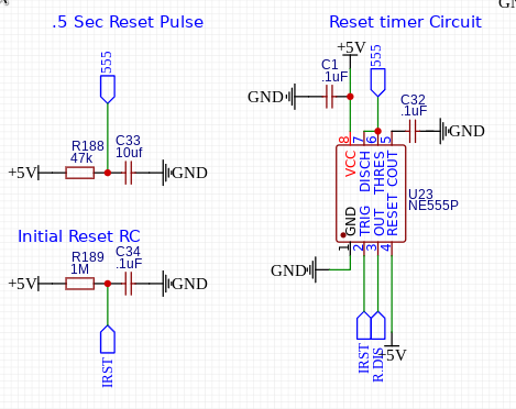
The resistor R11, and Trimmer R10 (combined with C7) provide the R-C network that makes up the main oscillator, as you can see this is essentially two Schmidt Trigger inverters tied together, the first with the resistors connected in feedback to create a very simple square wave oscillator. As I've discussed in previous Logs, this is a very common configuration for building an internal oscillator in a MCU, and has the benefit of being very "Parts Light". The reaming nets on the chip are used for generating Power On Reset (C1, R6 and ZD1), half step pulse (technically a single pulse generated by R9 and C3), and a de-bounced switch for the function select latch (C4 and R8).
the formula for frequency calculation is 1/RC ( in this case 2hz - 1.4khz ~ I did later end up using values to tune the eventual output to 2hz and 2khz -- though this came down to playing around with the values to find ones that produced this output.)
The power on reset signal, is simply a R-C circuit with a ziener diode that assures the signal is not sent to the inverter until it is at least 4.7v (de-triggering the input to a much higher threshold.) This has the added benefit of dropping the CPU into a continual reset state if the V+ rail drops below 4.7v in the case of a near over current situation.
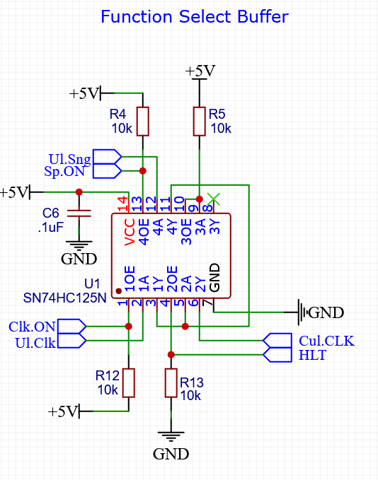
Function Select Buffer The function select is simply a Quad buffer package, the signals Clk.ON and Sp.ON are generated elsewhere (using a latch). The buffer holds both the Unlatched clock signal, and the single pulse clock in High-Z, using the pull up resistors at pins 1 and 13. We tie these signals low using a d-latch and it's Q and /Q outputs. The cumulative clock (either the unlatched clock or the single pulse clock, depending on the function latch) is held in an enabled state by pin 4 through a pull down resistor, and can be tied high using a HIGH signal latched elsewhere in the computer (most likely the flags register).
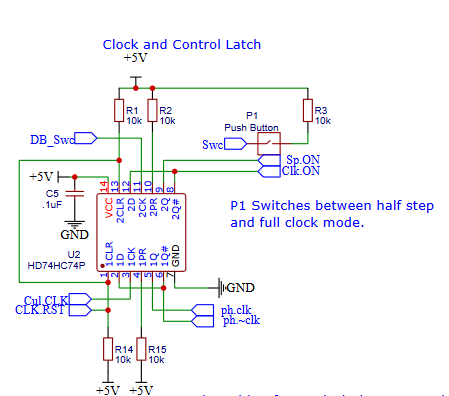
Clock and Control Latch
The clock and control latch is simply a dual d-latch, where both /Q outputs are tied to the D input (as shown above). The First takes the incoming cumulative clock signal from the buffer and divides it in half to produce our cleaned up clock pulses for the computer. The second uses a de-bounced switch signal at the clock pin to flip between the specific clock functions. These latches are placed in a default state by a power on reset signal generated at the inverter.
Latching the clock this way has all the above benefits of normalizing the clock, as well as saving the high sate of the clock through functional transitions and a halt. This is us full as we can see the state of all registers during a halt and a falling edge of a clock pulse generated by simply putting the clock into cut off won't cause unintentional errors.
Whats next?
I have plans to move on to building the accumulator for the ALU; this will be the first part of the build that uses a state machine to control the input to the 4 bit universal shift registers, these are needed vs a traditional d-latch as the ALU also supports a 1-bit rotate and shift operation. As always thank you for taking the time to look at my project, and feel free to ask any kind of questions that you might have in the comments. I hope everyone has a wonderful week, I'm finally feeling better and were on the trailing edge of the COVID infections that ran through our house over the last week, thankfully, the infections didn't turn out to be too bad or require any one of us to go to hospital, so for that I am very thankful.
A longer explanation of the completed clock module is forthcoming. A brief technical description of the module is available in the PDF of the schematics. For now the module:
keeps track of the state through transitions using a d-latch connected as a clock divider
switches between states using a single push button.
sends a momentary power on reset signal
accepts a high signal which when held high, the clock stops ( and holds it's state)
While waiting on parts for the prototype I had some time to work on the software end of the build. I made a slight change to my eeprom tool chain, and now I am happy to say I can build a .HEX file that supports the full minimum required address lines. This is due to adding support to overlay the data from another truth table by simply adding the data to the eeprom immediately after the primary data. The program is still very basic and I will be the first to admit that it probably has a few bugs but at least for the time being it appears that it correctly builds eeproms. When parts come in in the next week or so I should be able to build a rudimentary proof of concept and run testing. Additionally, I have drastically re-thought how a 74 series register can be used in the build, and switched to a 74HC194, this allows for performing all shift operations on the register, as opposed to using states within the eeprom. I believe this will significantly increase the chance of this very tricky to replicate behavior that would require a large number of control lines, or external decode logic to accomplish in the fist place. Speaking of control logic. I also built a truth table and spun a small hex file to properly handle much of the decode logic for operating the accumulator register properly. I have updated the files section with all the newest for your viewing pleasure; if you have any questions don't hesitate to ask
 Dave Collins

 The resistor R11, and Trimmer R10 (combined with C7) provide the R-C network that makes up the main oscillator, as you can see this is essentially two Schmidt Trigger inverters tied together, the first with the resistors connected in feedback to create a very simple square wave oscillator. As I've discussed in previous Logs, this is a very common configuration for building an internal oscillator in a MCU, and has the benefit of being very "Parts Light". The reaming nets on the chip are used for generating Power On Reset (C1, R6 and ZD1), half step pulse (technically a single pulse generated by R9 and C3), and a de-bounced switch for the function select latch (C4 and R8).