Dave Collins
-
Updated Proposed Clock Circut and Simplified Halt
01/14/2022 at 20:31 • 0 commentsHere is the updated clock schematic based on suggestions from the Facebook group Z80 DIY/Homebrew Computers & Projects, I have switched the capacitance values to much lower in order to be able to use larger value timing resistors. I don't think I mentioned the formula for calculating the frequency is 1.2 / R*C. The main issue with the last schematic is I forgot about the input current limits of the 74HC14N which are around 20mA. Using a minimum value timing resistor of 275 ohms, is pretty much required to limit the current to the input to a safe state below the current threshold of the input. Another suggestion was to use a ceramic cap for the R-C networks, since they are less susceptible to temperature change; and with the value much lower a better choice since they are far and away better performing caps, in terms of reliability. Another change I made was to tie the oscillation low using a transistor. this will halt the clock in full clock mode but leave the ability to single step, which will be useful for the state machine test bed program (you can do a single instruction jump to the next instruction which can augment the halt flag. Still not feeling up to building this up on the bread board, I've ordered 100K trimmers which won't arrive until at least Sunday. Hope everyone's weekend goes well.
-
Latched Clock Module without a 555
01/14/2022 at 04:40 • 0 commentsI'm nearing completion of the clock module for the prototype and the eventual build. This has 3 main goals:
- No 555 timer. (honestly if your module has a inverter why use a 555).
- Latch both CLK & ~CLK save the state through a halt and resume sequence.
- support a HLT on a HIGH signal from the CPU.
I completed a first draft of what I'm building in EasyEDA. I have tested most of the module and it works well. I will need to do further refinements to get it dialed in but its about 90% so I've uploaded a PDF of the working schematic. You can find it in the files section.
If you want a latched clock why no 555?To be honest; I don't really have a good answer beyond its been over done a million times. I had initially thought to build a op-amp oscillator but, opted (heh) to do an R-C inverter instead. The reason is simple; if your non-crystal clock design has an inverter, you should not use a 555, at least in my opinion.
![]()
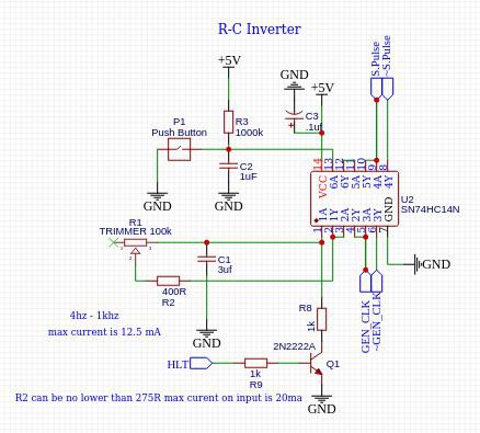
Simplified R-C Inverter Design Here is a over simplification of the clock's main astable oscillator. The first stage takes the RC oscillation (which appears on the scope as a triangular wave mostly; and outputs a result witch is more or less a rhomboid (and inverted). Since a waveform that is more or less a parallelogram is going to cause a problem for CMOS High levels, we feed this through a second stage, which flattens out the transitions and we get a nice square wave. The third stage is more or less just to get a inverted clock, although extra buffering is always nice on the thing you are going to hook to nearly every IC on your build. With 2 passives ( three when we wire in a trim pot), and 3 more inverters on the other side of the package to de-bounce a single step you can't really go wrong Full R-C Inverter Clock, with single pulse de-bounce.
![]()
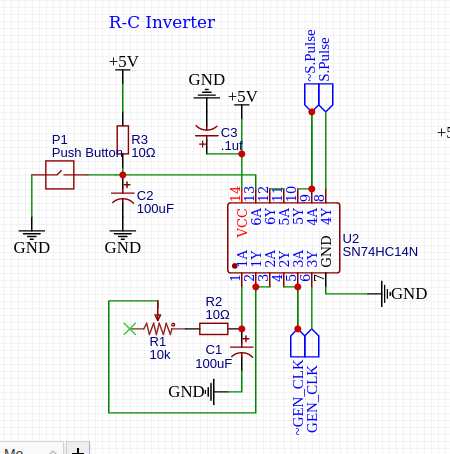
R-C Inverter clock with a de-bounced single pulse
In many, many, MCU's with internal oscillators this simple R-C and invert tactic is used. it produces a fairly decent nearly 50% duty cycle, though honestly this can be further refined. Another advantage to building the clock this way is we get full control of the added ~CLK signal off the output latch. By way of comparison, the ~Q output of the 555 timer latch is tied to an internal transistor in, and essentially discharged off to the ground.
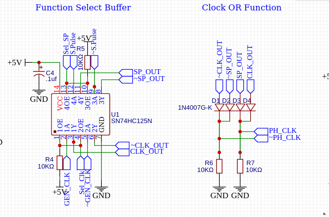
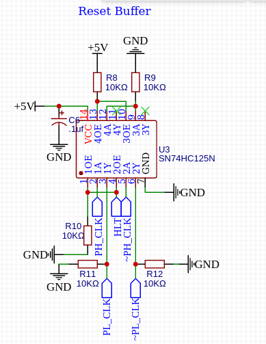
We can control the clock selection through a quad buffer (two sets for both ~CLK, CLK, Single Pulse, and ~Single Pulse), and a switch we de-bounce, elsewhere in the circuit. We tie the outputs together using a simple Diode/Resistor setup, in this case only, it's OK to leave the output of the tri-state buffer in tri-state as the OR gates are tied low on their outputs and do not actually care the difference between high Z and 0v (I think). I build the OR gates this way as two gates from diodes use slightly less tracks, and fewer power rails than a package with two terminated gates, which being in the clock module will likely not find use.![]()
Clock Selection Buffer
A second buffer takes the combined clock pulses to and from halt with a high pulse else-ware in the CPU; It's highly likely this part of the circuit will change drastically. I really don't like half using a package like this. It's possible I could bring the CPU to halt by grounding out both R-C circuits similar to the way James Cameron did in his pipeline CPU build; perhaps somebody who's taken the time to read all of this has a better idea?![]()
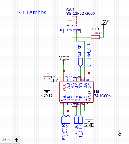
The S-R latch brings it all together in the end. One side of the Quad NAND gate handles the S-R latch for the clock, and the other handles the de-bounce for the switch that picks single pulse or the clock. I still have yet to build the HLT signal in place however, I get good oscillation out of the latch. I run into issues where the latch occasionally enters an unknown state brought on by both ~CLK/CLK being in full cut off. I have yet to figure this part out, i suspect the latch is oscillating at a very high rate but I require further testing. Additionally my tiny portable scope is more for automotive applications, so does not have a very high sample rate. After I have a finished prototype clock module that's fully built I will post a video.![]()
I am entering day three of unsettling unknown upper-respiratory viral infection, and so working on my laptop is generally the limit of what I can do right now, they tested for COVID but my results on the longer test haven't come back yet so I am stuck at home while we verify. And so i don't get co-workers and family members sick, I am isolating away from my work bench (which i doubt I'd have the mental clarity to work at in any case).
Hopefully you found my ramblings entertaining or interesting at the very least. I rattled off a lot of self-taught nonsense in the above; so take that with a huge grain of salt. If anybody is willing to set me straight; or tell me my design is rubbish and how, to fix it I am all ears. Have a great week everybody :) -
First draft of .HEX files completed
01/05/2022 at 19:58 • 0 commentsI've completed 2 FSM descriptions in logism, and built source from that. From here, I will burn a pair of eeproms and see how they perform on the bread board with a pair of 4 bit latches. I expect this to be completed by weeks end but as im working on this in spare time its possible to take longer.
The UFS4057ES - A 4 bit ALU / CPU Build
Building a small computer with an EEPROM brain.