Timings are crucial! Let's check if we can go with a 4MHz clock using 70nS SRAM and the EEPROM.
CPU timings
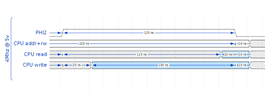
First of all I want to try to recap CPU informations about timings from the WDC W65c02s datasheet.
In the picture:
- PHI2: at 4MHz clock speed each PHI2 phase lasts 125nS for a total time of 250nS.
- CPU addr+rw: setup time for A0-A15 and RW signals is 20nS; this happens after 10nS from the PHI2 HIGH-to-LOW transition.
- CPU read: data acquisition happens after 115nS from PHI2 LOW-to-HIGH transition and it lasts 20nS.
- CPU write: data exposure begins after 25nS from PHI2 LOW-to-HIGH transition and it lasts 110nS.

Let's zoom now into PHI2 HIGH phase:

It's very important to observe what happens after the PHI2 HIGH-to-LOW transition:
- CPU read: the CPU requires no data changes for 10ns.
- CPU write: the CPU holds data stable for 10ns.
PLD delay
PLD, as you already know now, handles all the glue logic; there is a propagation delay introduced by the ATF22V10C-15 (max 15nS) but this should have no practical effects on timings.
RAM timings
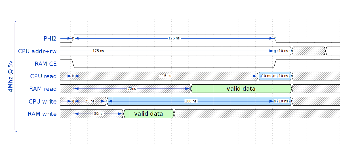
In the next picture:
- RAM CE: PLD select the RAM (CE goes LOW) when the address matches and PHI2 goes HIGH; this will result in a (almost ***) perfect match.
- RAM read: RAM presents stable data after 70nS from selection (CE goes LOW) .
- RAM write: RAM requires to have stable data after 30nS from selection (CE goes LOW) .

(almost ***): can we have problems when RAM CE goes HIGH but CPU is still reading for additional 10nS?
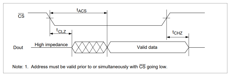
From RAM datasheet:

When CS goes HIGH the RAM hold valid data for tCHZ time that should be from 0nS to 25nS so we need to test RAM access @4Mhz to verify if this is true and if it can be a real or a pratical problem.
Perhaps the PLD propagation delay (15uS) could save us here, I don't know... (tests are required).
EEPROM timings
Let's check now the AT28C256-15 EEPROM:
- ROM CE: PLD select the ROM (CE goes LOW) when the address matches (without considering PHI2).
- ROM read: ROM presents stable data after 150nS from selection (CE goes LOW) .

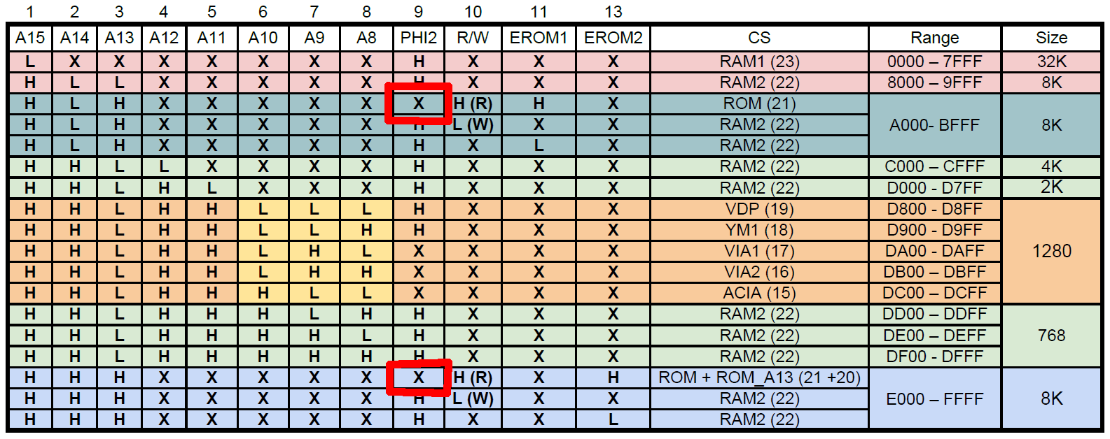
I have to update the PLD glue logic table applying the changes in red:

Next step: RAM/ROM test on access
Let me know what do you think in the comments...
Ciao!
PS:
I would like to thank everyone who sent join requests for the project. I'm considering whether or not to accept some collaborations maybe a little further on. Commenting on posts is already a way to collaborate and to help me. Many many thanks!
 padnest
Discussions
Become a Hackaday.io Member
Create an account to leave a comment. Already have an account? Log In.