-
Do it right....
01/08/2023 at 16:31 • 0 commentsFirst prototype had a few main issues that blocked the project for some time:
- Problematic LED placement on the side - they didn't fit due to the plating thickness.
- A lot of sidelights that light up the next element in a stack.
- Bad design of castellated holes.
- Absence of the mounting features for acrylic parts.
- Acrylic parts by themselves.
Before going too much into details and design decisions, I want to say an enormous "Thank You" to PCBWay for sponsoring the new PCB design and helping me with my design questions.
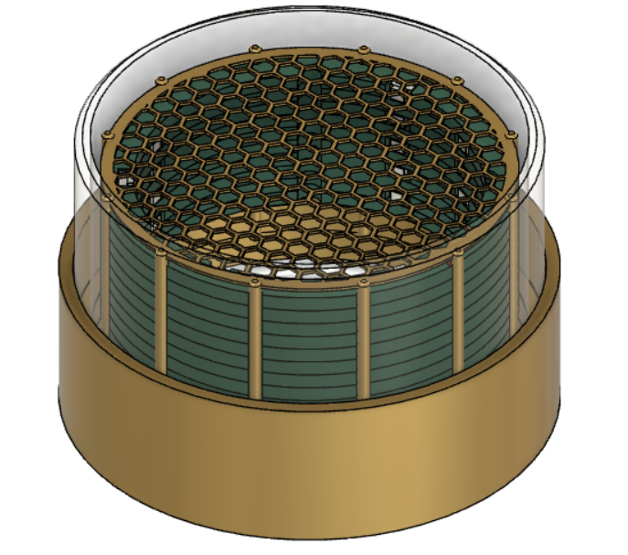
From a previous iteration, I learned one super important lesson which is "Don't start without a proper plan". So I designed the end device in Fusion360 to have a visual representation of the whole assembly, and it helped me a lot during the design process!
![]()
---------- more ----------
![]()
Let's go through all of the issues that were described above one by one.
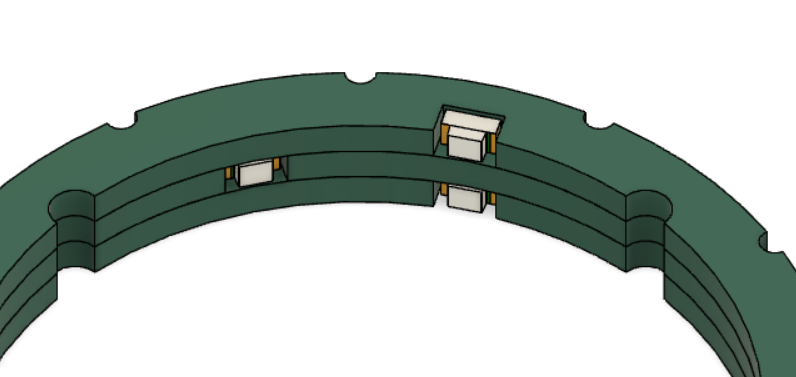
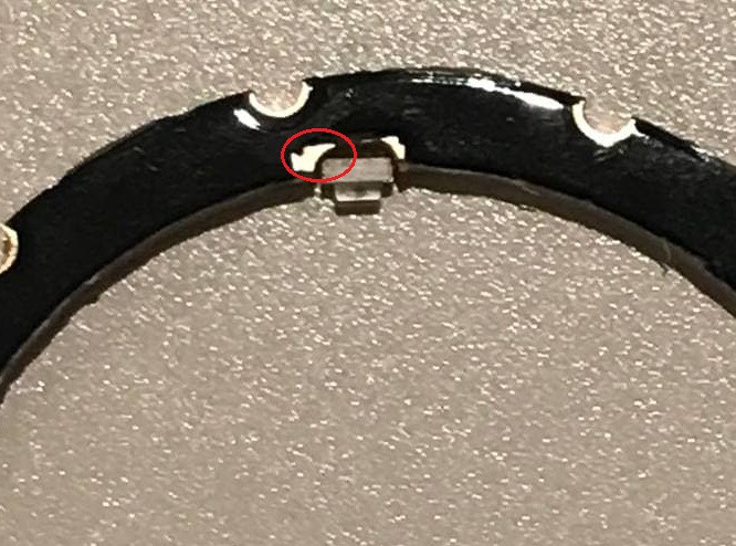
- The problem with LED placement was easy to fix. I changed the footprint for the LED to compensate for gold plating, put the LED deeper, and added the vias in corners to compensate for the radius of a cutting tool.
- There was also an easy fix for an incorrect design of the edge plating and castellated holes - I just followed these two guidelines from PCBWay webpage for castellated holes and edge plating.
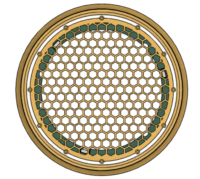
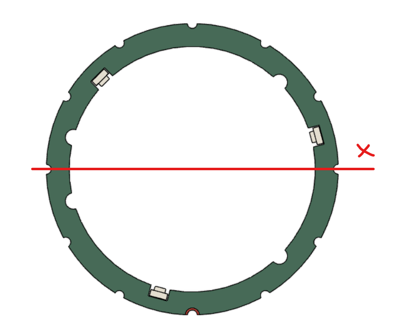
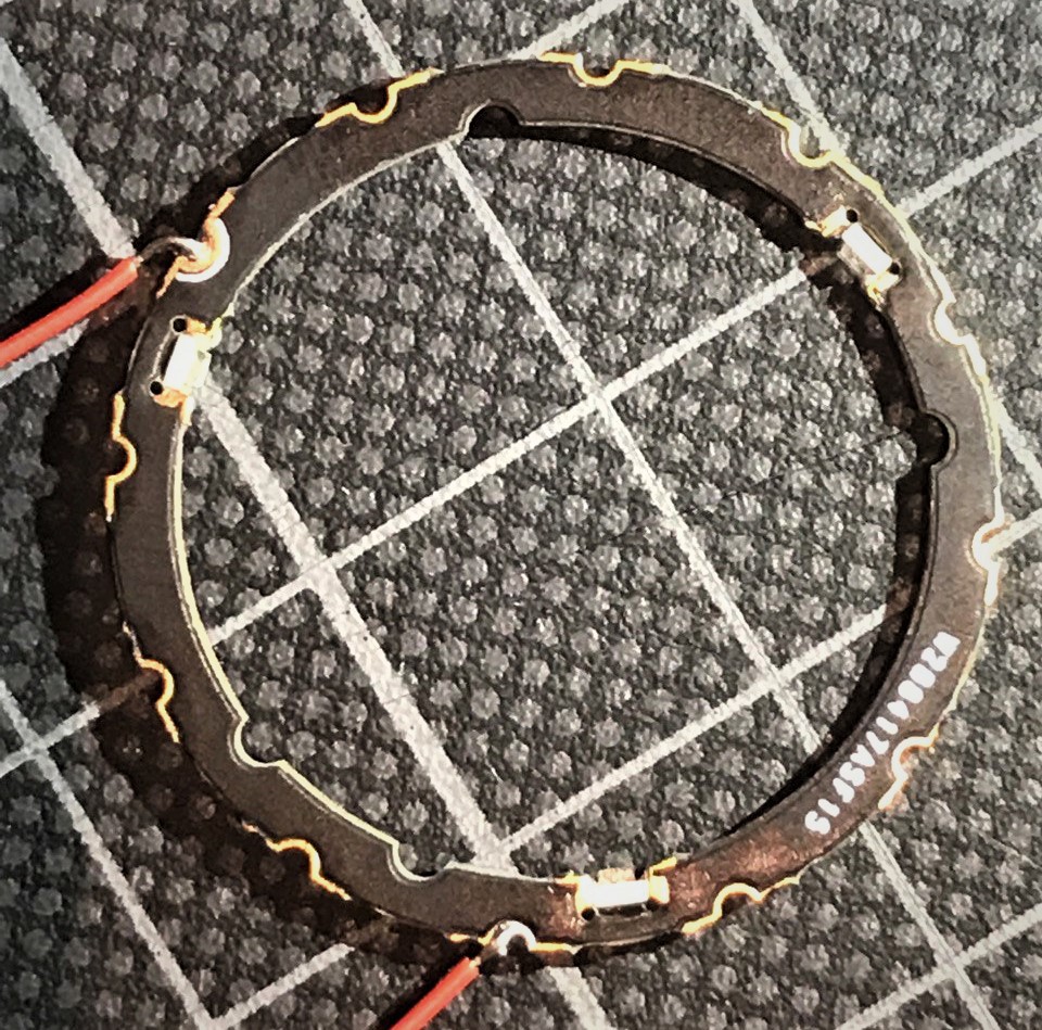
- Sidelight emission and the absence of mounting features for acrylic parts were fixed with what I call a "flippable" PCB. The new PCB is designed in a symmetric way, which means that I can flip the PCB around the x-axis and have the mounting half-holes in the same position.
![]()
This approach gave me the possibility to use the same PCB to prevent sidelight from a previous segment and reduced the cost of the design as a whole (gold-plated edges are expensive!). Now I can use one PCB instead of two, as it was in the initial idea.
![]()
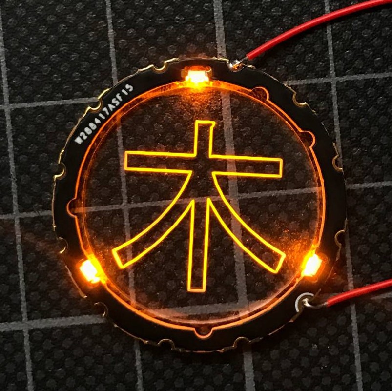
After fixing all these issues and designing the whole assembly in CAD, making a new PCB was super easy - simply exporting DXF, placing holes and LEDs on already predefined spots.
Two weeks after that I received my PCBs from PCBWay! As expected, boards look nice and all previous issues are gone.
![]()
![]()
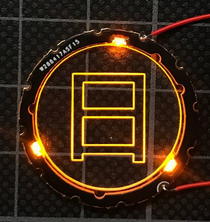
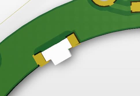
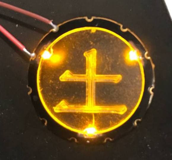
LEDs are fitting perfectly this time:
![]()
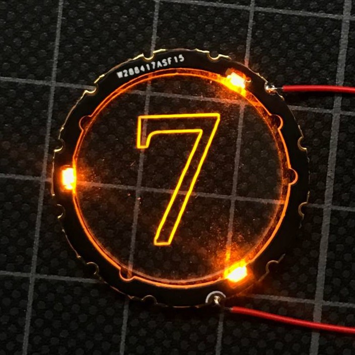
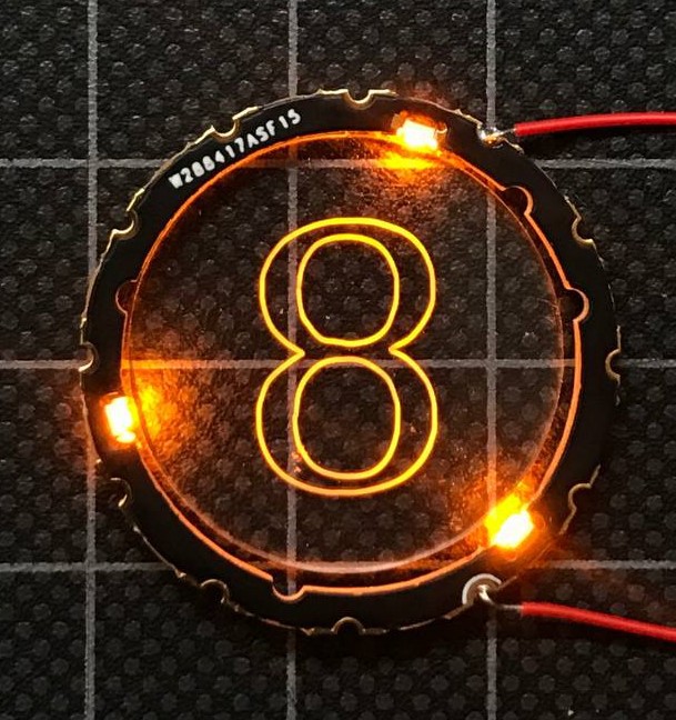
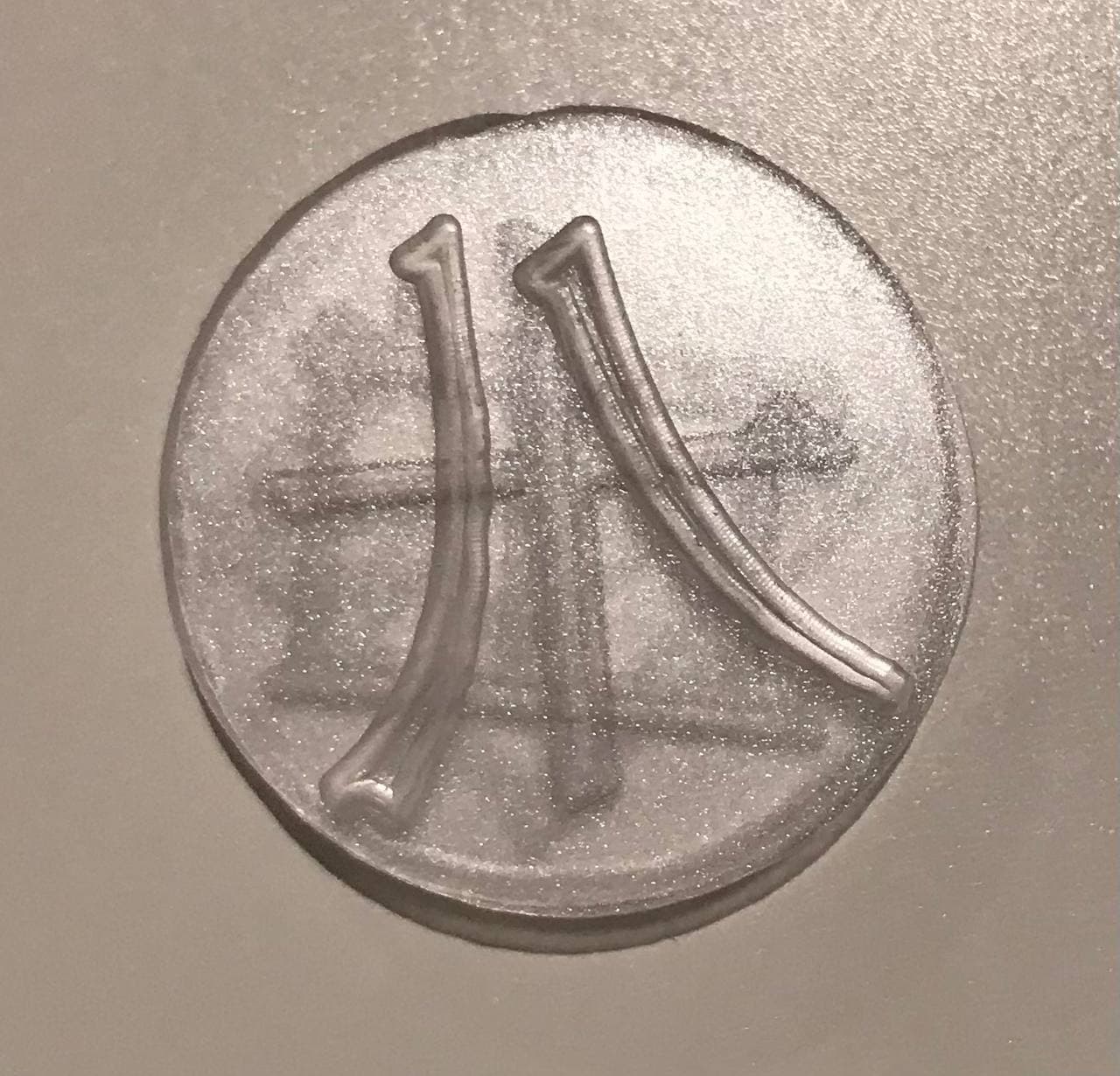
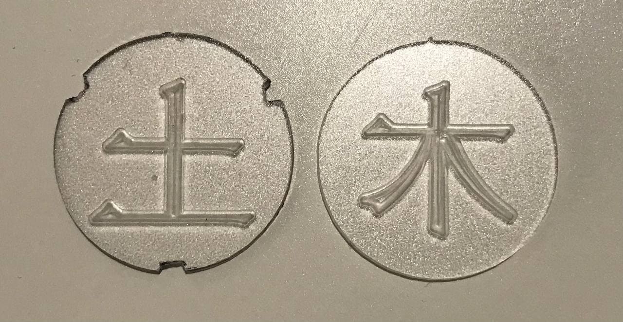
And the last problem in the design was the acrylic parts. I ordered some samples some time ago before redesigning the PCB. They are smaller than the new ring and don't have mounting features but they are still a good visual representation of the final result.
![]()
![]()
![]()
![]()
The next steps will be ordering proper acrylic parts and making the first full assembly. I hope that these small steps will not take another year))
And finally, I want to thank PCBWay once more for supporting this development. If you are looking for a PCB manufacturer for your project PCBWay would be definitely my first recommendation!
Cheers...
-
First try...... and fail)
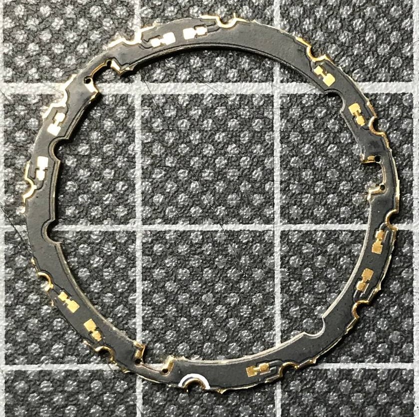
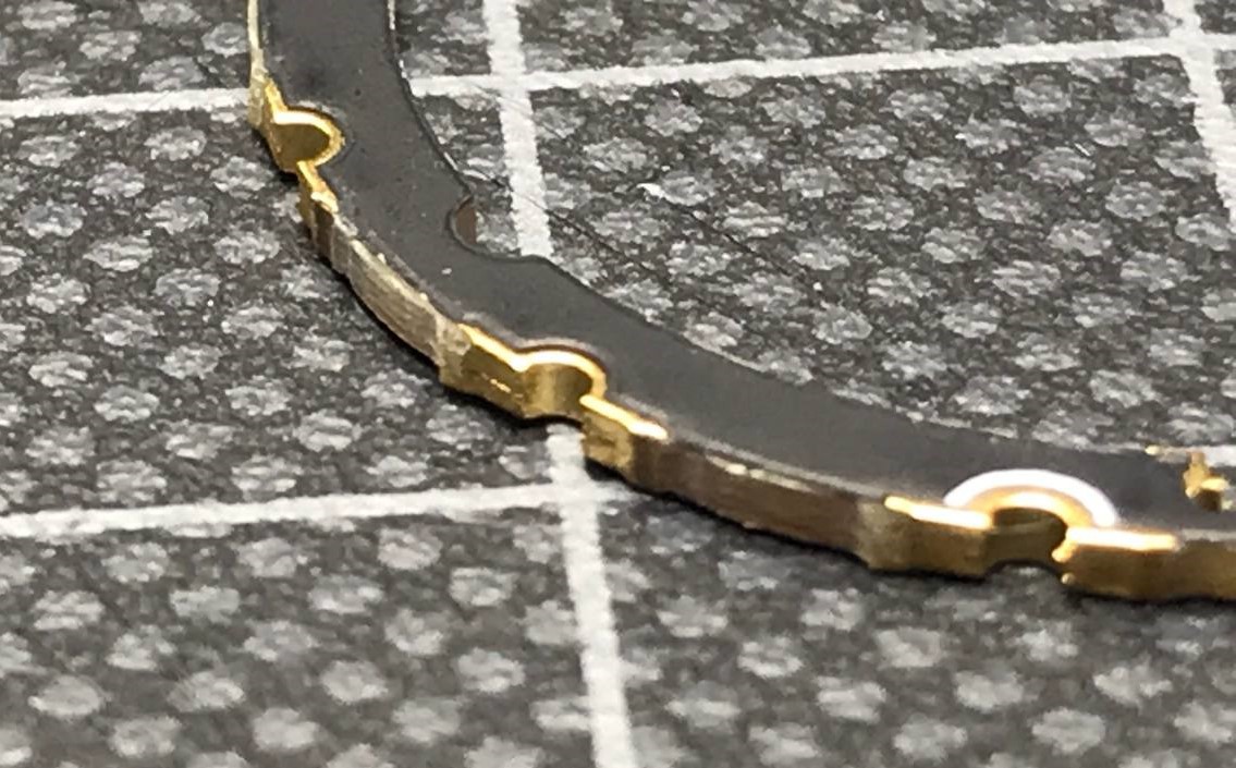
01/24/2022 at 21:30 • 0 commentsTo implement this design, I came up with an idea of a ring PCB that would hold 3 side-mounted LEDs on the inner side and castellated holes on the outer side to connect all PCBs together and to drive signals. Designing this PCB I forgot about two very important things.
The first one is that the milling tool that cuts a PCB has a big radius, which is kinda catastrophic for such small holes and slots as in my design.
![]()
![]()
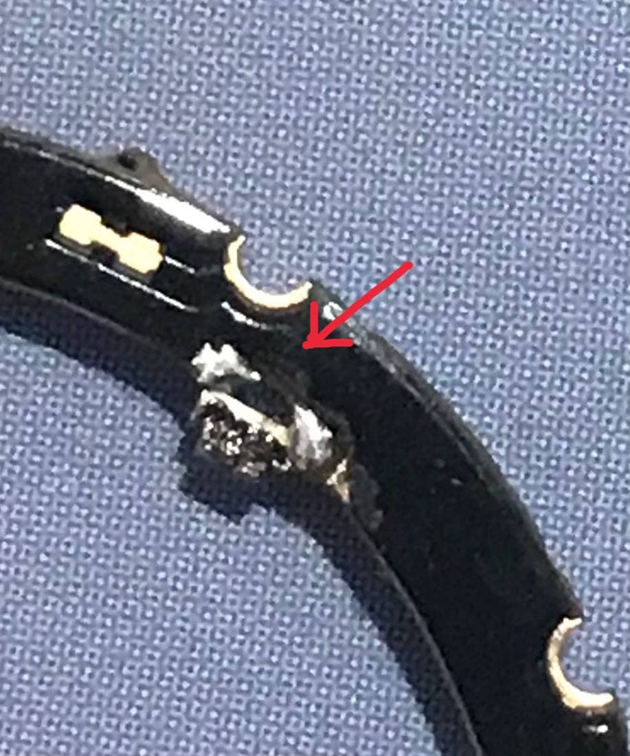
And a second one - gold plating also adds extra thickness. As a result, my LEDs didn't fit at all. The gap between PCB and LED was HUGE! You can clearly see that in the next photo where I tried to solder them.
![]()
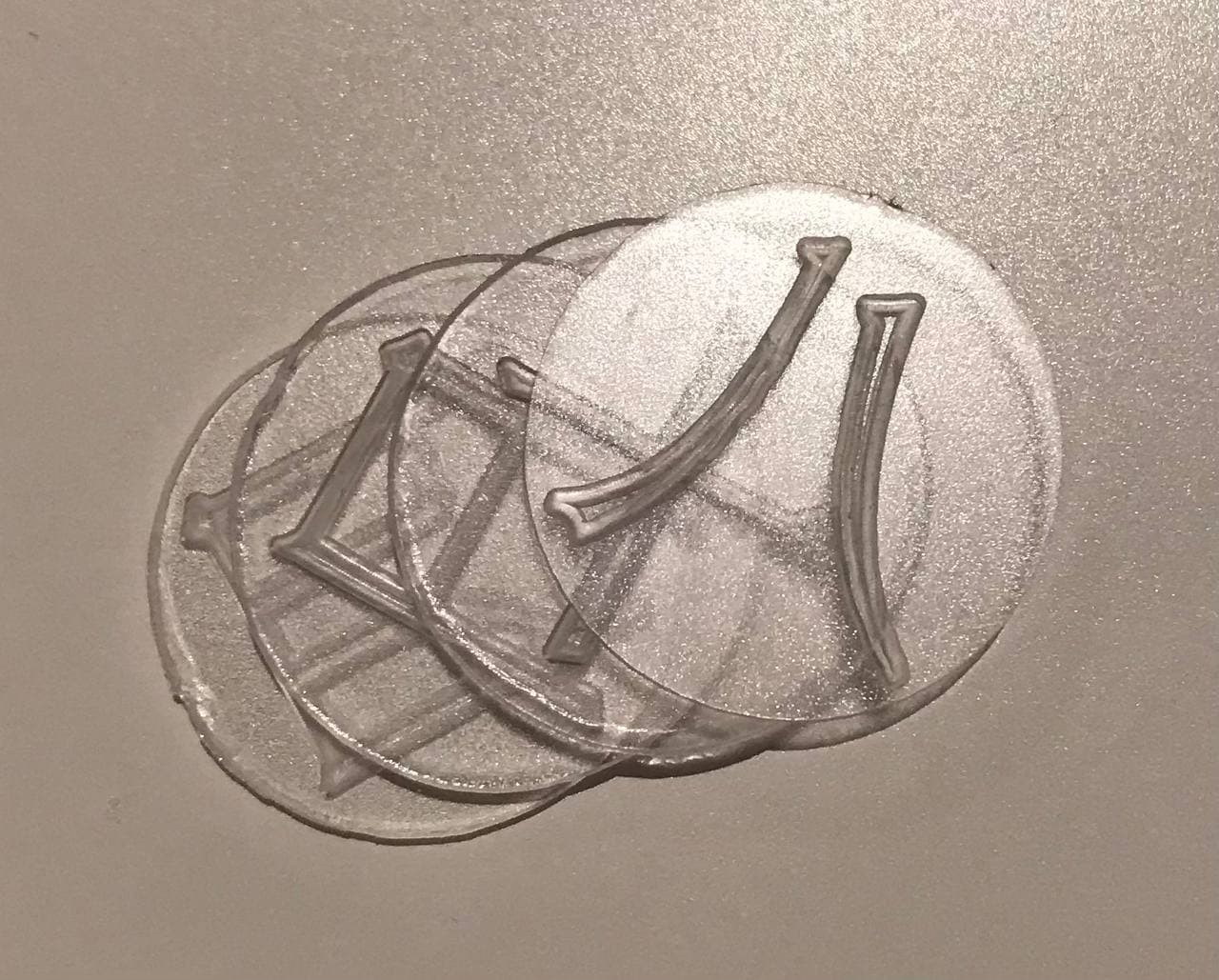
At the same time for the first prototype, I made acrylic parts using a CNC machine. It wasn't a good idea. Probably because of the milling cutter, settings, or small dimensions, engraving on acrylics looks very rough. And one side of that acrylic is with antiglare effect. So.......it is unlikely that I will see the last symbol in a bunch. (proper testing still needed)
Four disks stacked on top of each other:
![]()
![]()
To fit an acrylic disk to PCB with "mounted" LEDs I had to use a scalpel to cut small slots in the disk.
![]()
As a result, I got a lot of sidelights that would also light up the previous and next symbols in the assembly. Although, honestly speaking, it happened not only because of these cut slots, but also due to LEDs being put not deep enough into PCB. To solve all that I should have made two different versions of the same board with slightly shifted LEDs, which means that the next board in the assembly would cover the previous one and prevent from undesirable light.
![]()
As for the first iteration, I'd count this result as a small success, mostly to cheer myself a little bit up :)
Before designing the new version of PCBs still have a lot to test. Mostly will order central pieces with laser engraving and will try different materials. Also want to assemble everything together and put it into a test tube that I'm using as an enclosure.
Will keep you posted.
JIXIE - Small LED Nixie Tube
Inspired by Rodan-Okaya GR-524 Nixie Tube