Eric Ljungquist
-
Basic Building Blocks
02/21/2022 at 07:31 • 0 commentsNMOS-Resistor Logic, Dynamic Logic
This log goes over what I call the basic building blocks of the circuit.
I chose NMOS logic as it seemed very straight forward to design with. I've also seen a lot of designs using BJT Transistor-Transistor Logic to build discrete component circuits and I wanted to do something a bit different.
Basic Logic Gates

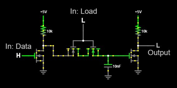
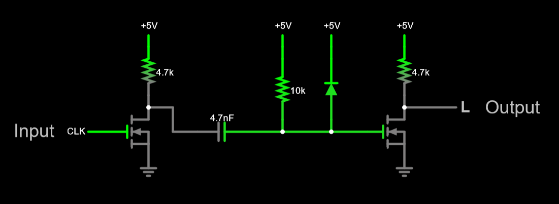
D Latch
![]()
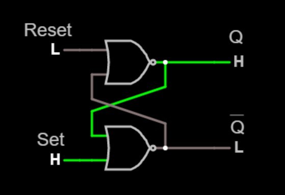
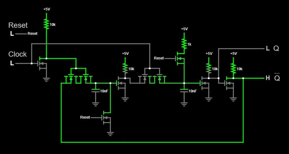
SR Latch
The SR latch is a simple way save a state. e.g. "Do I have data in the buffer I need to send?" or "Am I currently sending out a data packet?". I used the typical two cross coupled NOR gates to implement mine. At power up the latch will start in an unknown state. I've added an additional pull down mosfet to the "Set" side of the latch to act as an additional input for the power-on-reset circuit.
![]()
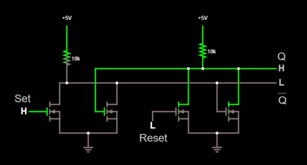
The transistor level diagram:
![]()
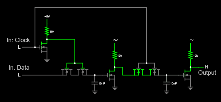
D Flip-Flop
For the D Flip-Flop we are just doubling up the D Latch shown above in a master-slave configuration but with a slight change to the Load input. This prevents the flip-flop from being "transparent" while clocking in the data signal.
![]()
Edge Detector
![]()
-
Control Logic
02/21/2022 at 07:30 • 0 commentstemp
-
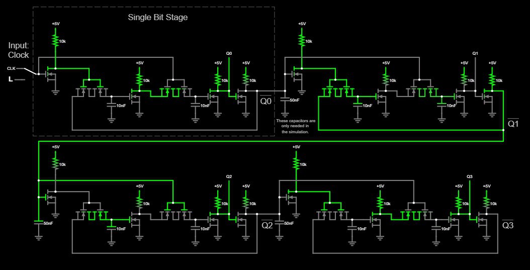
4 Bit Counter
02/21/2022 at 07:29 • 0 commentsThe above video show to early testing of the counter. I have it hooked up to a 555 timer and the outputs of each counter stage are connected to an LED. The LED's show the circuit count up in binary as expected.
![]()
kl;kj;
![]()
jk;kj;
-
8 Bit Buffer
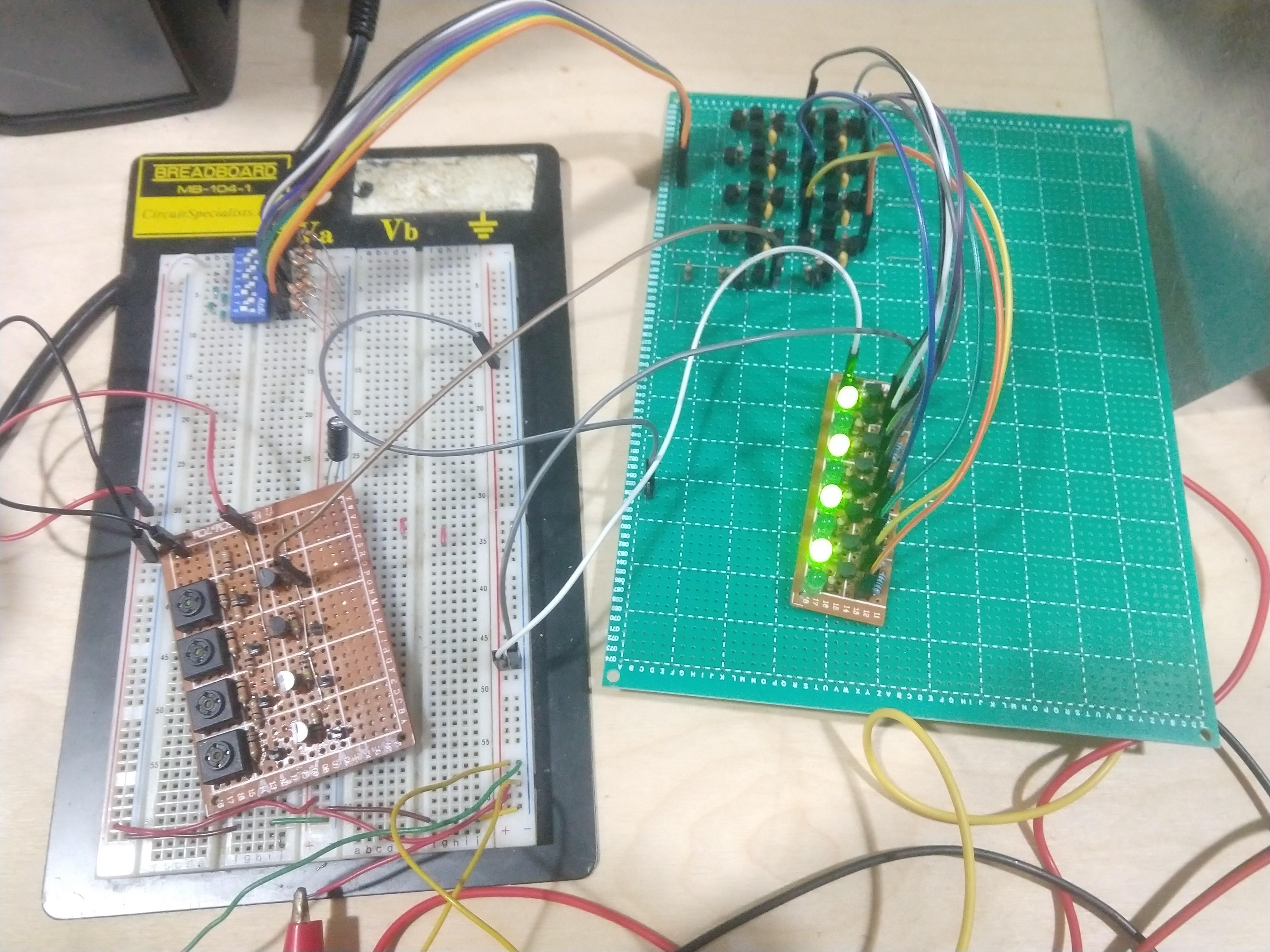
02/21/2022 at 07:28 • 0 comments![]()
I don't have much to say for this section. I only included it as I had taken the above picture showing some early testing. In the image I am testing that each latch was holding data correctly. I didn't have any issues with using dynamic logic to store the data. In testing I found that the value would only bleed off or on through the transistor switch after two to five minutes. Much longer than what was needed for correct operation.
![]()
The 8 bit data buffer is implemented the same as what is outlined in the project log "Basic Building Blocks" under the Data Latch heading. The circuit is just copied and pasted eight times over.
-
Parallel In Serial Out Shift Register
02/21/2022 at 07:26 • 0 comments
Parallel-In-Serial-Out Shift Register in CircuitJSThe Parallel-In-Serial-Out Shift Register is the heart of the project. Most of the other circuits are there to control the state of the shift register.
I implemented the shift register as the standard D Flip-Flop chain. I added a D Flip-Flop for every bit I needed to send, plus one flip-flop for the Start bit, and one more flip-flop as an output stage. The Stop bit doesn't get its own flip-flop, once the last bit is sent out of the shift register, any further clocks output a High signal. The state counter just runs for an extra cycle past the last data bit sent.
To implement a loadable D Flip-Flop I took the basic D Flip-Flop outlined in the "Basic Building Blocks" project log and added a mosfet switch leading to the capacitor on the slave side of the flip-flop. This allows the charge of the capacitor to be set independently of the clock. The outputs of the 1 bit data buffer feed directly into the transistor switches of each shift register stage. The output stage holds the last value that was clocked in so that the output of the shift register does not automatically change when loading the rest of the flip-flops. Not shown in the above diagram is that I added a mosfet controlled pull-up on the output stage to act as a "Set Pin". This set pin is pulled high when the transmitter is not running so that the output is held at the "Idle" State. -
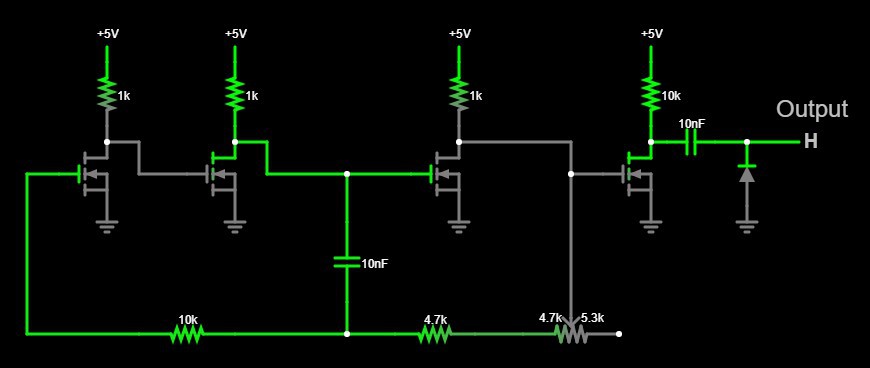
Clock Generator
02/21/2022 at 07:09 • 0 comments![]()
Clock Generator in CircuitJS I wanted the board to generate it's own clock. I felt like the board would be a more complete package if included and didn't seem to be much of an issue to add. I came across Fairchild's Application Note 118 quickly in my search. The application note details a Ring Oscillator that is slowed by an RC circuit on the feedback line. It looked like exactly like what I needed, low parts count and can fit the NMOS logic theme.
To allow calibration I've added a multi-turn potentiometer on the right side of the feedback line so that adjustment to the output frequency can be made.
I breadboarded it up and it seemed to work just fine looking at the signal on the oscilloscope. I just had to add an inverter to the end to help square up the output waveform. At the time I wasn't sure what frequency I would end up using. I was planning for 9800Hz but wasn't sure if everything would work at that speed. To test the rest of the circuit before settling on a clock I used either a button to single step or my signal generator. This ended up being a bit of a problem for me as I thought that the clock would work perfectly when dropped in. I designed the rest of the layout while only leaving myself just enough room to add what I had already came up with for the clock.
I had everything working correctly while using the external clock from a signal generator. I then rebuilt the clock circuit on a breadboard and fed the output into the rest of the project and it did not run at all. I hooked the project back up to the signal generator to help debug and determined that a DC offset on the low voltage state of the clock was causing some major issues. I found that if the low side of the clock was above about 160mV then the rest of the project would not change state correctly. The low voltage portion of the clock signal was fluctuating between 180mV to 250mV. I was able to squeeze in a coupling capacitor on the output which got the offset down to about 10-30mV. After this addition, things started working correctly.
The clock signal still has some pretty bad ringing on it that I think are causing some minor issues but for the most part it works.
Serial Transmitter Using Discrete Parts
An asynchronous serial transmitter using only mosfets, resistors, capacitors, and diodes as building blocks.