[EM] = Electronic Modelling

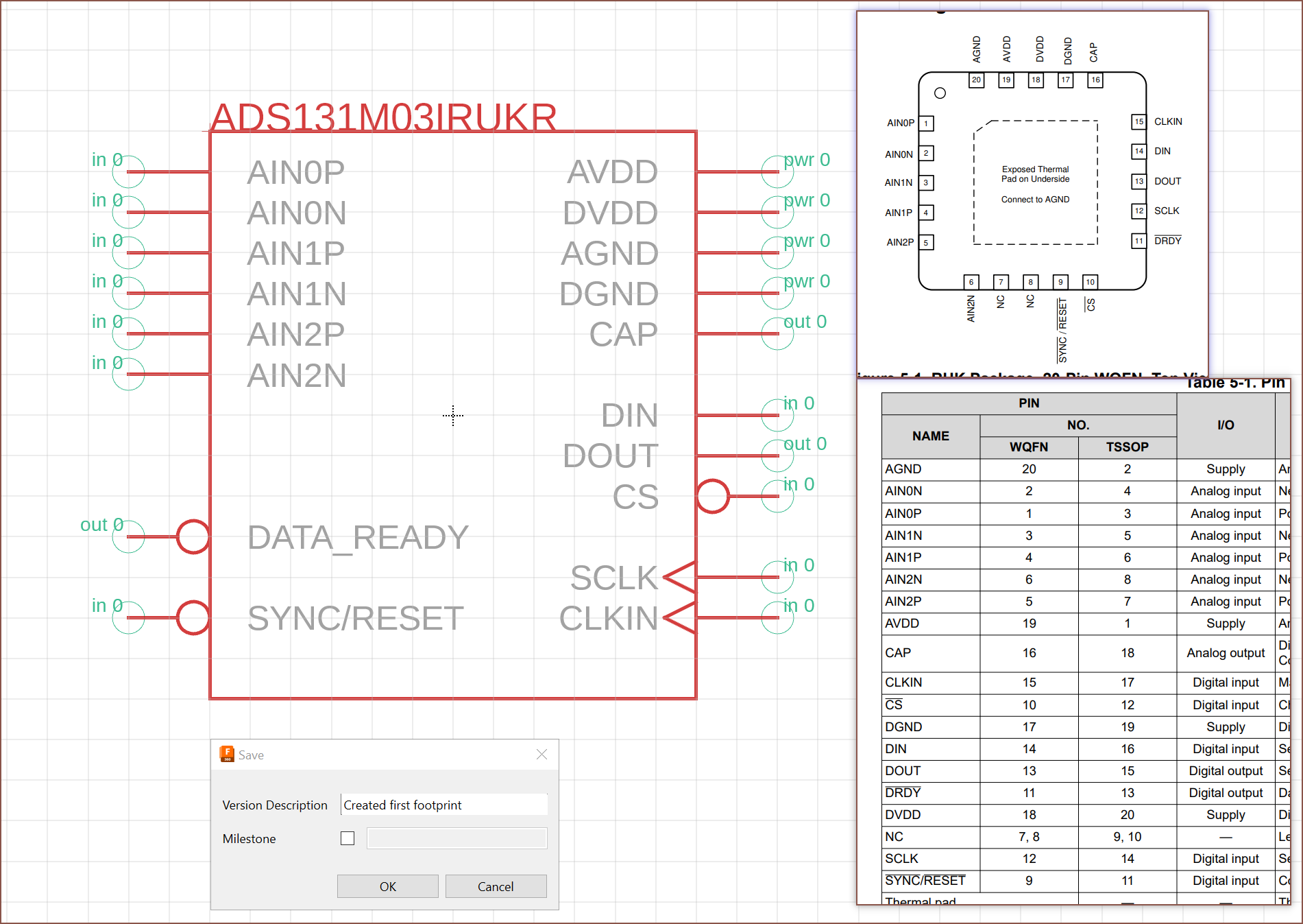
So, probably 2 hours after deciding that it's probably time to start working on the PCB, I've got my first symbol.
Some things I've learned:
- While asked many times on the forum, the Fusion 360 team has no desire to implement KiCAD library imports.
- Apparently, this is something holding back users that want to create custom keyboards.
- Speaking of custom keyboards, I looked online for a split keyboard (to compare with the Lets Split I built for £81 and barely used) and everything is usually bland-looking and either large (because of the numpad), over £100 or both.
- I guess this half explains why I've got to invent a brand new input device here, despite engineers around the world with better credentials and surely working on more complex problems seemingly content with being landlocked to a desk, potentially with some pay2play tweaks (as seen on r/mk or r/ergomk). It seems that there's just not many companies in this input device business, and innovation from established players seems to be non-existent.
- Apparently, this is something holding back users that want to create custom keyboards.
- There are keyboard shortcuts for adding a pin and naming it.
- There's a "Pin Array" which basically makes this entire IC symbol for you, and I didn't know about it until I was like 2/3rds into creation.
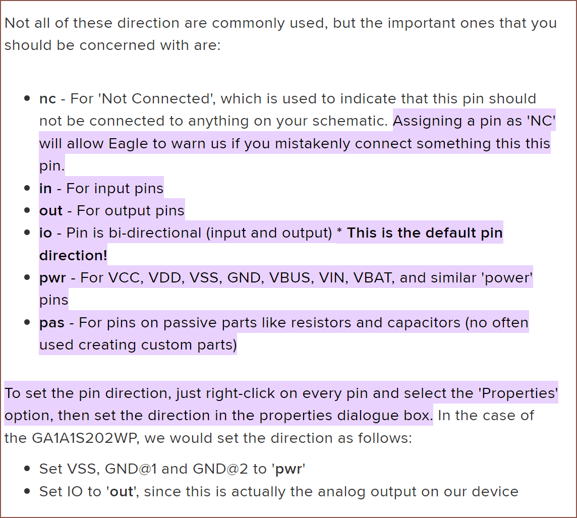
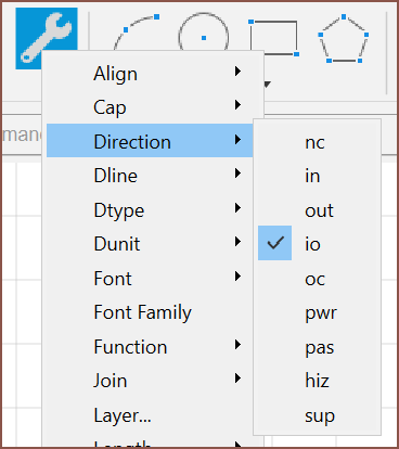
- There's some mysterious list of "Pin Directions" (see my mention of the "Change" command) and I can't find any docs on the ones that are Fusion360 exclusives (aka didn't feature in EAGLE).
- There's a "Change" comand that means that I can select what I want to change in a menu, then click on the pin I want changed.
- For example, instead of right clicking each individual pin and then clicking properties and then clicking Pin Direction and then changing "io" to "in" (because that's what I did), I can just set up the Change function and then quickly click the pins I want to change.
I can only imagine that "hiz" = High Z = high impedance. No clue what "oc" is.
Things to mention:
- I assume I can treat the components library similar to how I create a BOM folder for normal modelling.
- Next steps are to create and connect the footprint and 3D model.
- I couldn't really find any specific IC symbol layout guide to conform to, so I just tried grouping similar pins together and I think what I've created looks easy on the eyes.
- Creating this custom component first is like a low level mob fight before I go to the high level boss: the custom-footprint ESP32-S3-MINI-1U.
- (custom as in it's not a regular package like QFNXX that can be auto generated by Fusion, as well as having the most pins out of all components)
 kelvinA


Discussions
Become a Hackaday.io Member
Create an account to leave a comment. Already have an account? Log In.