Close
0%
0%

DIY 1.3 GHz FET Probe

An active scope probe with high-ish bandwidth and very low input capacitance

Similar projects worth following
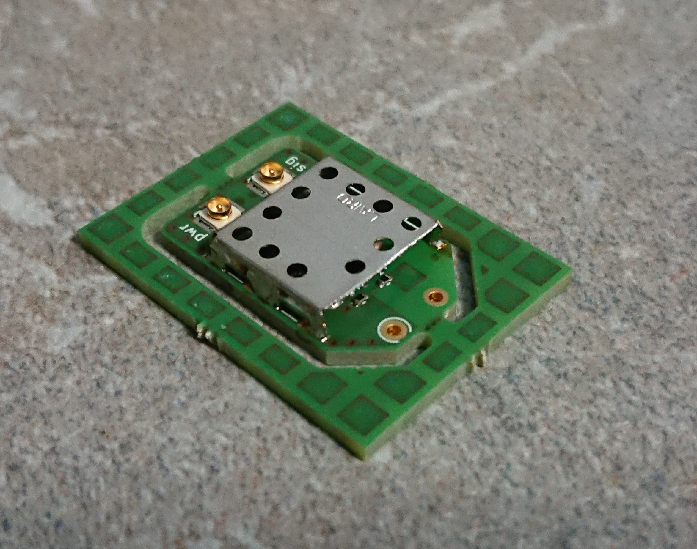
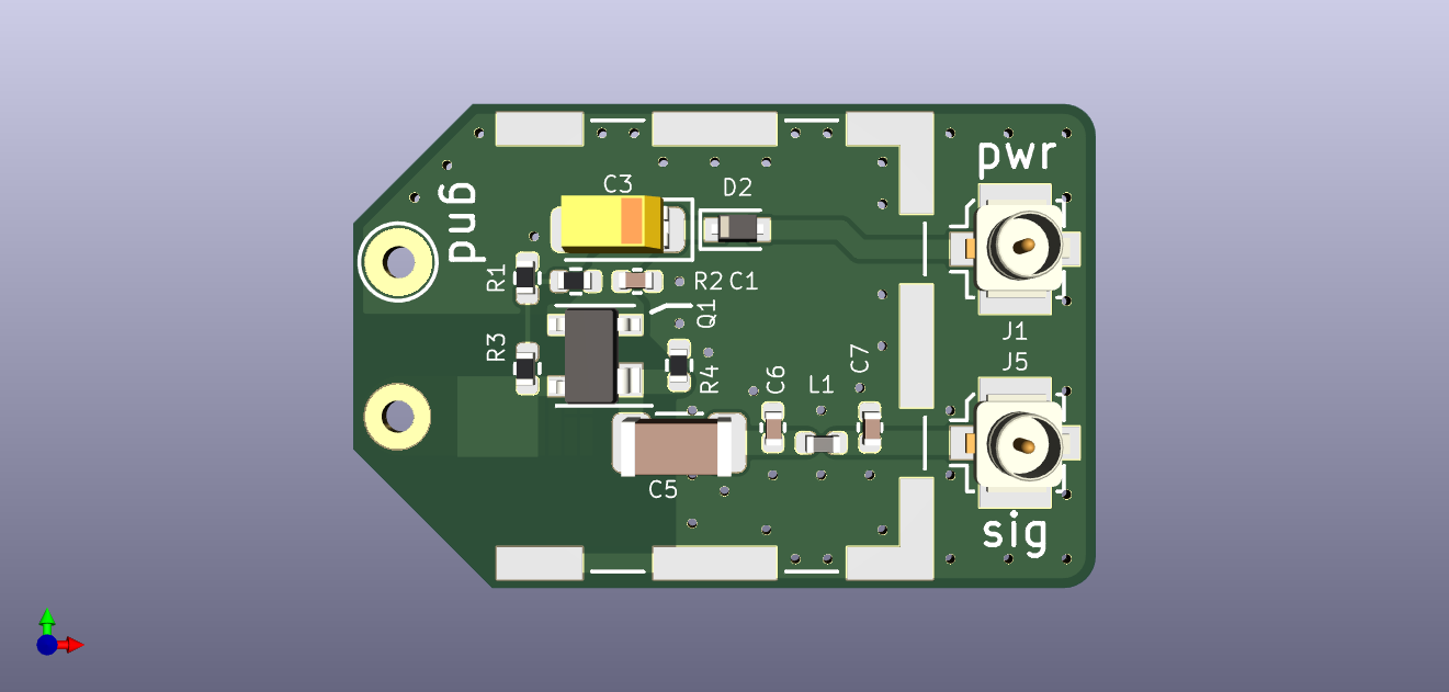
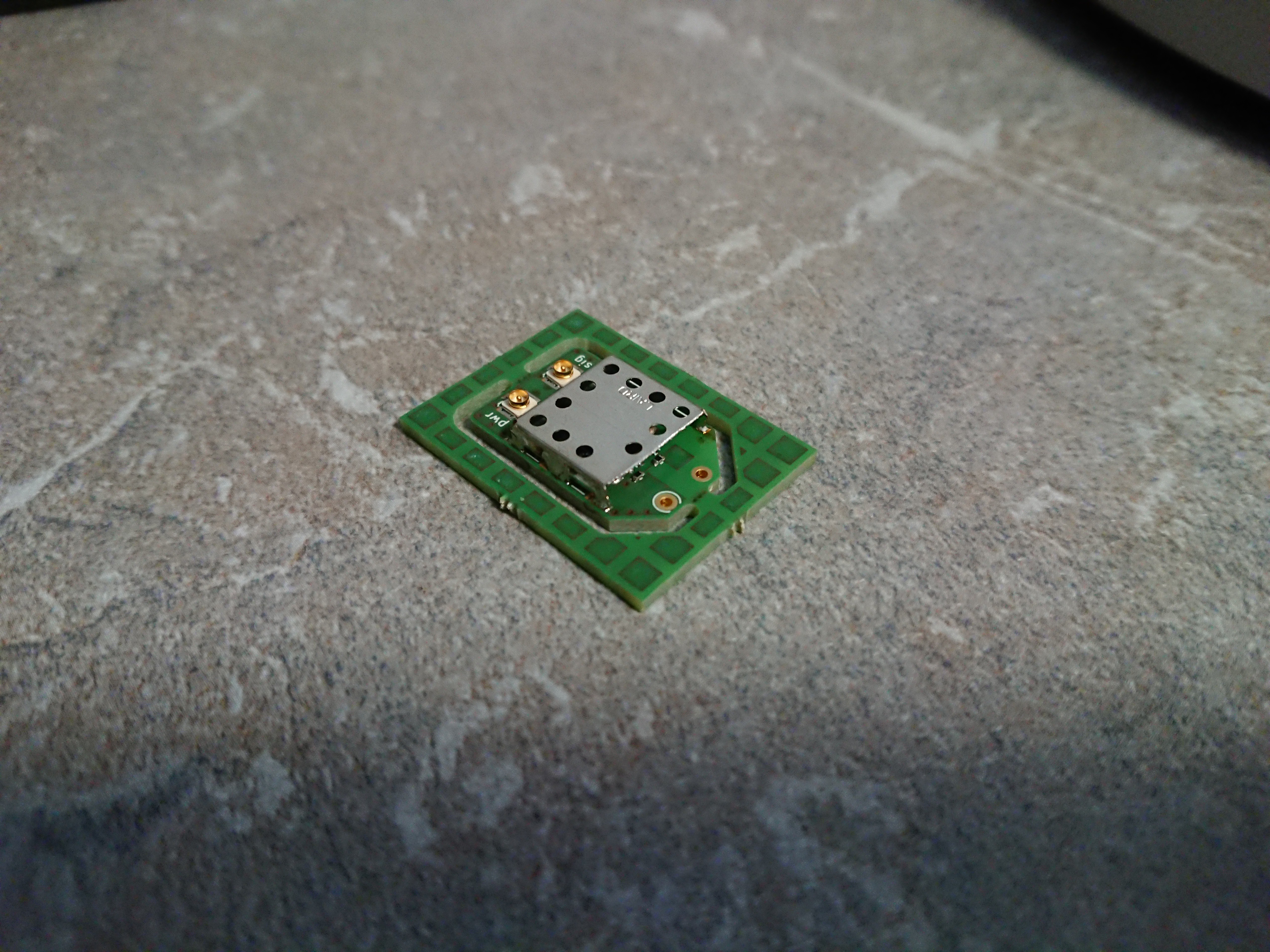
I wanted to see if an oscillator in one of my circuits was actually oscillating - so I needed a probe with low capacitance. That's why I was looking for such a thing, and I found the design that this probe is based on. It's built around the BF998 dual gate FET, and these are the probe's main properties:

- input capacitance: 0.3 ... 0.4 pF
- AC coupled, starting at around 100 kHz
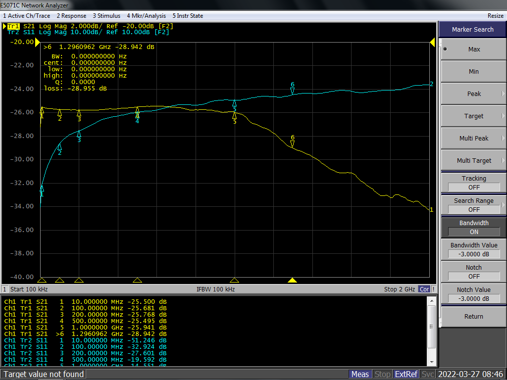
- bandwidth: 1.3 GHz
- Attenuation: 10x without termination, 20x into a 50 Ohm load (roughly)
- supply: 5V, 50 mA through u.Fl
- output: through u.Fl
- designed to be small and light
- flat bottom so you can stick it somewhere close to your measurement location and solder it in

I needed a scope probe with low input capacitance for the following use case:

In one of my projects, I wasn't sure if a crystal oscillator was actually oscillating. Probing with the stock probes that came with my Rigol DS1054Z didn't seem like such a good idea. The probe has about 10 pF of capacitance, and the crystal's nominal load capacitance is about 7 pF - that's a problem. If it's loaded correectly, attaching the probe might stop it. If the load is too little, attaching the probe might allow the oscillator to oscillate at all. So a probe with low input capacitance was needed (this is not a sound assessment of the situation, I just guessed that).

Looking for ready designs online revealed a design from a bachelor's thesis, which I adapted a bit. In fact, it had already been picked up by Wolfgang:

https://electronicprojectsforfun.wordpress.com/rf-measurement-techniques/high-frequency-probes/

After I (re-)designed the PCB, I sent one to him for some measurements. Bandwidth is indeed about 1.3 GHz:
If you want to read a bit more:

https://electronicprojectsforfun.wordpress.com/solder-in-probes/

  • Attenuation at low frequencies (50 - 100 kHz)

    Christoph10/09/2024 at 13:47 0 comments

    I was asked if the probe can be used below 100 kHz. So I took one of the older ones I had around and had a look at it with the scope.

    • Input to the probe: Signal generator, sine, 5 Vpp into 50 Ohm, at varying frequencies starting with 1 MHz and then from 100 kHz down to 50 kHz in 10 kHz steps.
    • Output to the scope, terminated with 50 Ohm, scope set to 20x
    • Then another round with the input cap enlargened by solder-blobbing it.

    Before:

    After (modified):

    Result table:

    So with the larger input cap the attenuation at low frequencies is around -25 to -26 dB, as desired. However, input capacitance is somewhat larger (but still low - but I don't know how low exactly).

  • Slightly misapplied: High side FET gate input

    Christoph01/21/2023 at 21:03 0 comments

    The only low-capacitance probe I currently have is one of these FET Probes. And I had to have a look at the gate signal for a high-side FET in a BLDC motor controller. So why not try it with this one!

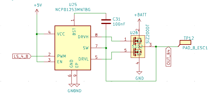
    Here's the schematic for the gate driver and dual FET for one of this controller's motor phase outputs:

    We want the gate signals to be clean: If they are too slow or wobbly, they might keep their FET in the linear range for longer than necessary, resulting in higher dissipation. The goal is a tidy step from "off" to "on".

    While the motor phase is low, the gate driver can charge the bootstrap capacitor (C31 in the schematic) and then use the charge in that capacitor to switch the high side gate. When it's on, the motor phase will be at battery voltage and the capacitor floats above that. Any extra capacitance from probing will distort the signal, so we want to use a low capacitance probe like this FETProbe.

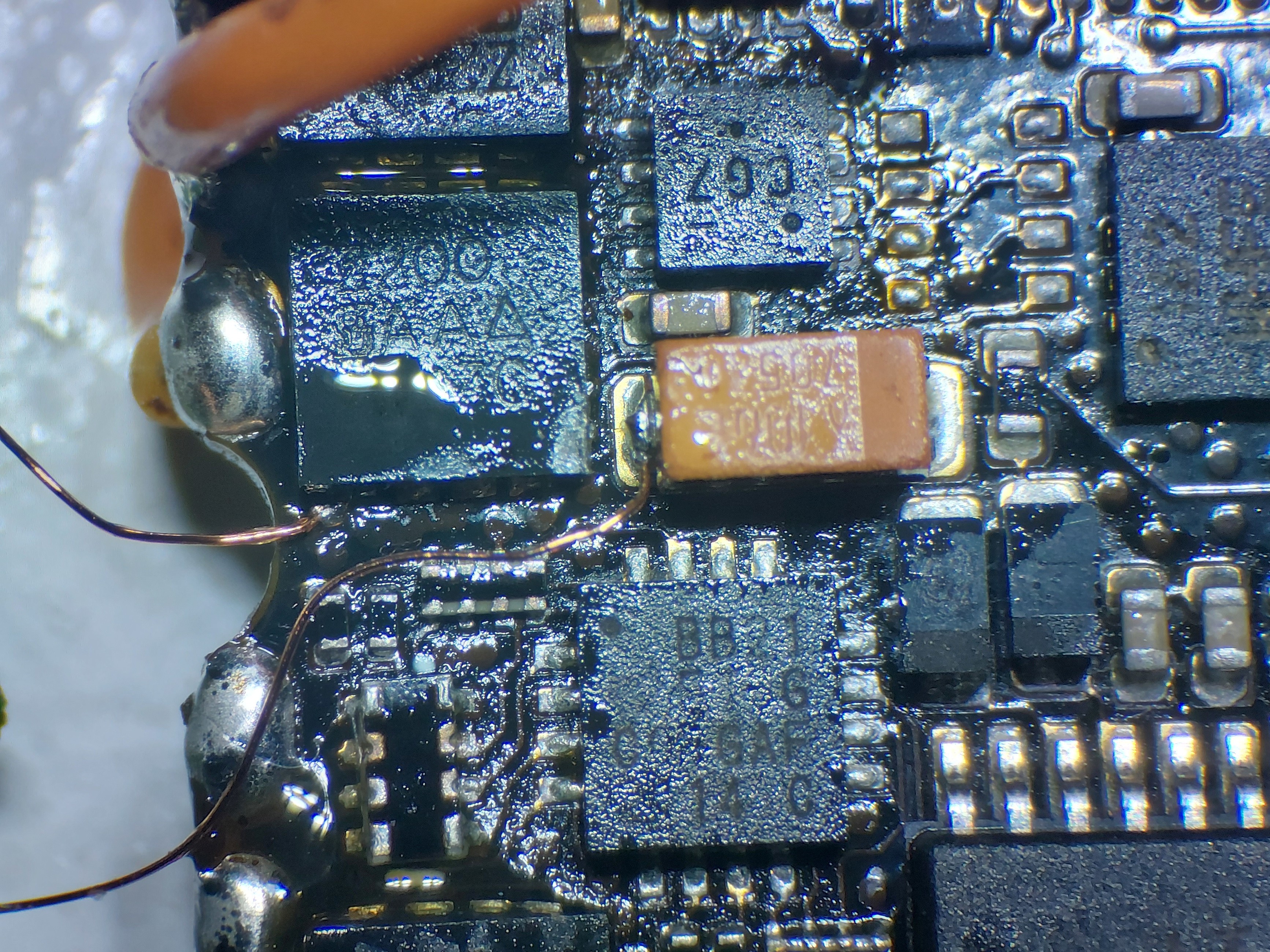
    Soldering it into the device under test

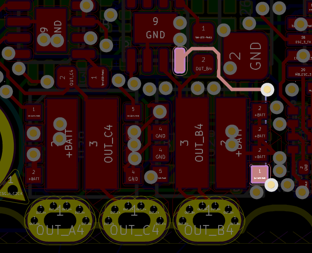
    It's not that simple in this case, because the layout is pretty dense, but I found a good candidate which was even one of the longer gate signal traces in this design.

    The gate signal layout:

    With the probe attached, let's see what comes out of it. We have +BATT = 8V, so ideally the gate would float at 8 V and get switched to 13 V during the "on" time.

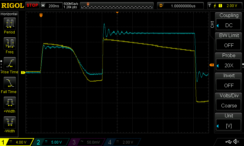
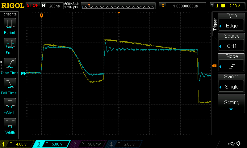
    Here's a screenshot that shows the FETProbe's output AND that of a passive probe on the high side gate input:

    Ch1 (yellow): FETProbe
    Ch2: passive probe for reference

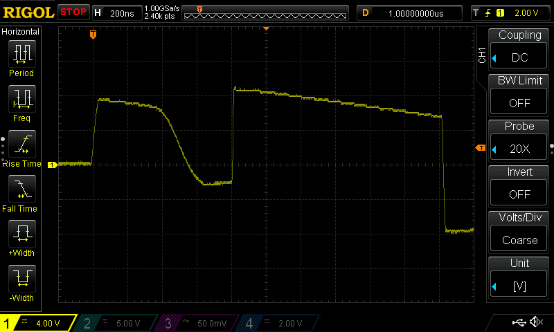
    In the first half we can see the controller's deadtime insertion. It's running bluejay firmware compiled for 40 deadtime units (roughly 800 ns, 4 horizontal divs). During this time, the phase is left floating and then drops to ground. After that, the high side FET is switch on and its gate jumps to around 8+5 V = 13 V. We can see that in the passive probe's output. However, the passive probe has high input capacitance and shows some wobbling. When we remove the passive probe, we get this from the FETProbe:

    Looks pretty similar - really nothing to see here: the main takeaway is that the gate signal is pretty stable and clean. The ramps come from the FETProbe's AC coupling, and there's nothing we can do about this.

    With the passive probe free, I decided to add the actual switching node to the scope screen:

    It's indeed switching between 0V and 8V, as expected, and the high side gate follows the switch node unless switched on.

    Of course, DC coupled differential or single ended probes would be a better match for this task, but that's a different story.

  • Measuring an SX1280's oscillator frequency

    Christoph11/02/2022 at 21:41 0 comments

    My initial use case for a low capacitance probe was this: Is the oscillator of an SX1280 (RF Chip) on my PCB actually oscillating with the right frequency?

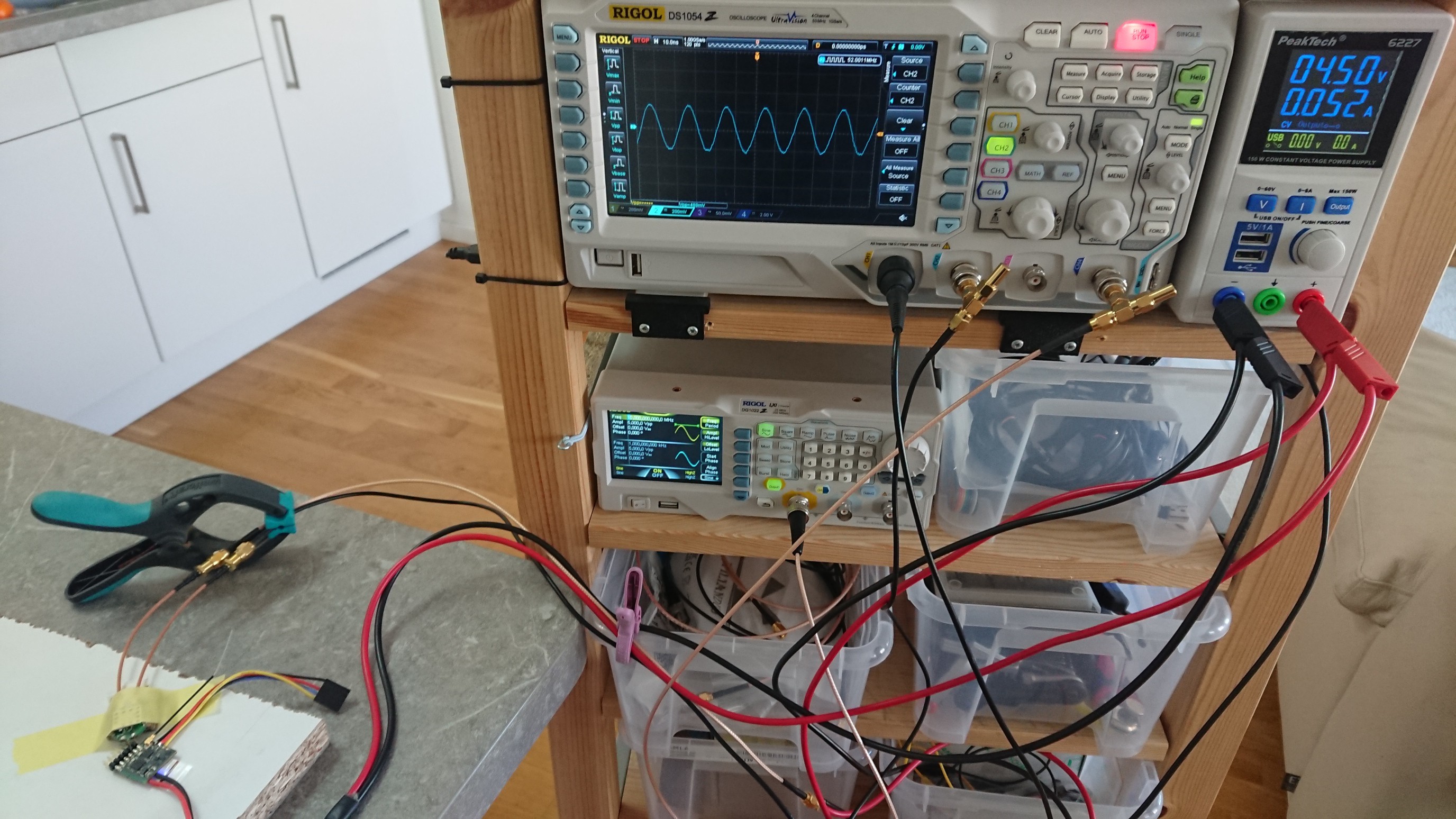
    The setup:

    A bit messy, ok. We have

    • a power supply for the probe and the device under test (DUT)
    • a signal generator (DG1022Z)
    • an oscilloscope (DS1054Z)
    • the DUT
    • and the FETProbe
    • plus some cables

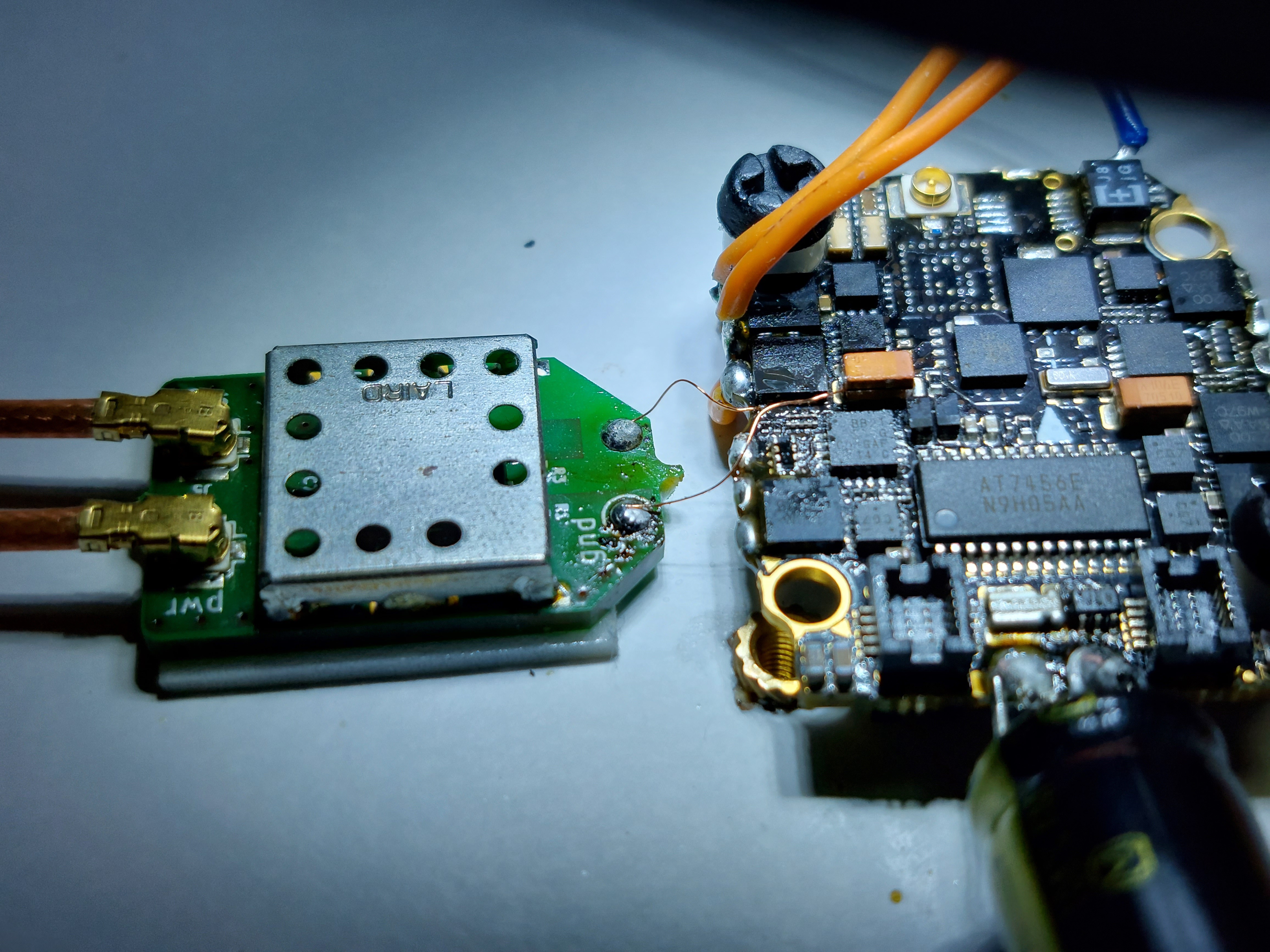
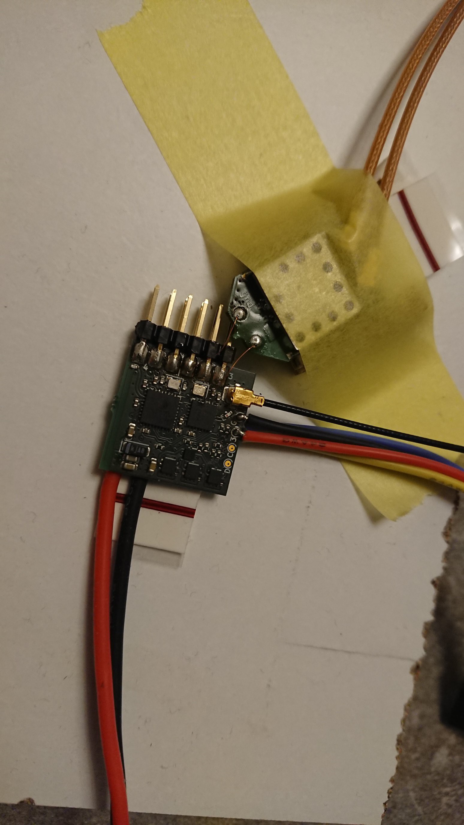
    Closeup of the DUT and probe:

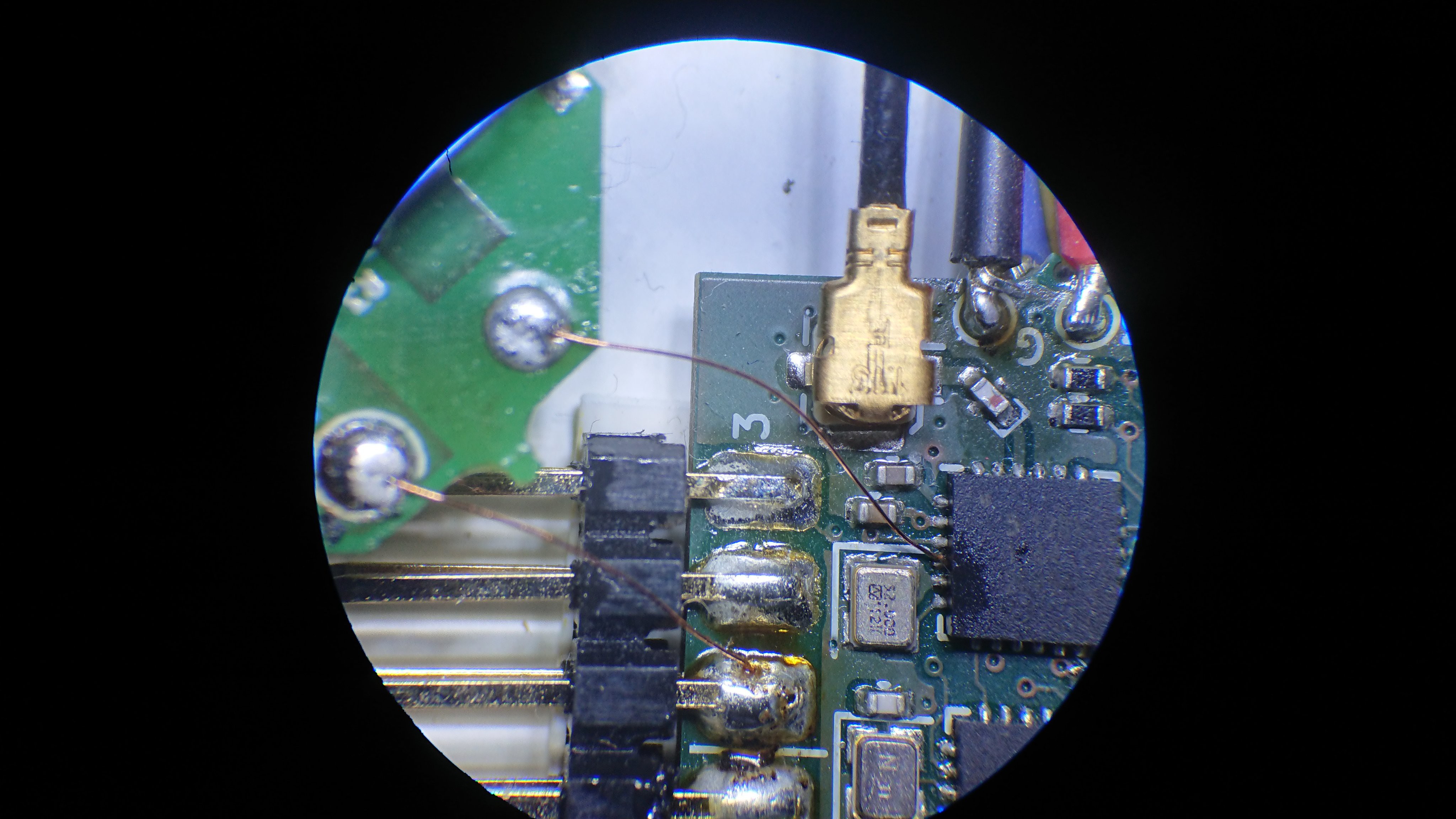
    And even closer:

    The crystal in the DUT is a 52 MHz, 10 ppm part.

    First of all it's important to note that the scope's timebase isn't terribly accurate at +/- 25 ppm. Trying to get meaningful numbers for a 10 ppm crystal won't go too well without a more accurate reference. That's why I added the signal generator to the setup, because its timebase has only +/- 1 ppm. Both devices also had half an hour of time to get to temperature.

    Making a reference measurement

    • Signal generator set to 10 MHz, 5 Vpp, sine output
    • Fed into a scope channel
    • Scope configured to use its frequency counter to measure the frequency

    The scope reported those 10 MHz as 10.0002 MHz in the display. That means that the scope's timebase is running a bit slower by roughly -20 ppm if we assume the signal generator to be accurate. That's still within the +/- 25 ppm stated in the datasheet.

    So whatever frequency it reports for further measurements, the actual measured frequency will be roughly 20 ppm slower than what is displayed.

    Measuring with a passive probe

    The stock passive probe (PVP2150) set to 10X gives us 52.0003 MHz displayed. Adjusting for the scope's timebase error, that's 51.99926 MHz actual frequency or -14.2 ppm. Amplitude roughly 0.5 Vpp.

    That would be out of tolerance for the application. In really bad cases, the probe's input capacitance could even stop the oscillator.

    Measuring with the FETProbe

    With the FETProbe, the scope displayed 52.0011 MHz. Again adjusting for the timebase error, we get 52.00006 MHz actual frequency or +1.2 ppm. That's much better! Amplitude was also around 0.5 Vpp.

    The FETProbe's low load on the circuit really made a difference here.

  • Effect of termination on the probe output

    Christoph09/12/2022 at 21:39 0 comments

    This probe's attenuation isn't very accurate, especially without termination on the scope end. I've had a look at what the termination does.

    The setup

    Probe in a fixture, with one SMA coming from a signal generator, and the other going to the scope (channel 1, unfortunately hidden behind the probe. The fixture looks just like the unused one to the left). Probe output also goes to the scope (channel 2):

    Probe is supplied with a bench PSU set to 5 V. The other fixture shown in the picture is not in use.

    Signal generator

    • 1 MHz sine
    • 5 Vpp
    • zero DC offset
    • High-Z load

    Scope

    • time: 200 ns/div
    • vertical: 1 V/div
    • Channel 1: input from signal generator, no termination
    • Channel 2: FETProbe output, through a T, to add a termination resistor later.

    Results

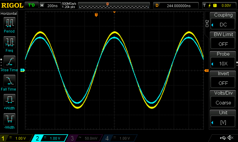
    If there's no termination, channel 2 must be set for a 10x probe. Here's the result:

    That's an error of about two subdivisions, or 0.4 V (-16% with regard to 2V5 peak). Not so pretty - we'd like the two signals to have the same amplitude. Or at least a little less bad.

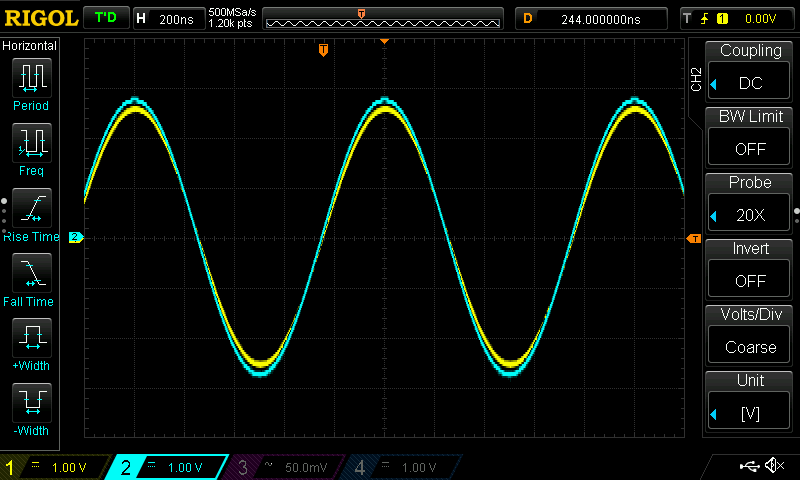
    With termination and channel 2 set to 20x:

    Zooming in, I get about 1 subdivision of overshoot, or +8%. That's better.

    More expensive professional probes are of course better in this regard, and I'll try to find ways to improve this one. It's definitely a good start, considering that it's cheaper than the passive probes that come with an entry level scope. 

    Further remarks

    Also note that the probe doesn't really care about its input signal's DC offset. Since the input is fed straight into a series capacitor, it's stripped from its DC part. That's why it can handle signals that swing below ground, as in this case (signal generator is set to zero DC offset).

    The probe's output filter also begins with a series capacitor, so the actual output to the scope can also swing below ground even with a single +5V supply. It's inherently AC coupled, so it doesn't matter if the scope is set to AC or DC coupling. And no, we cannot measure DC signals with this thing.

  • Aluminium enclosure for a handheld version from PCBWay!

    Christoph08/14/2022 at 20:36 1 comment

    I wanted to make a handheld version of this probe, so a fellow maker designed an enclosure that was big enough to hold, and also big enough for other probe designs. 

    PCBWay offers CNC parts, including surface treatment like anodizing. It's not as cheap as ordering PCBs, but still affordable. Also, PCBWay sponsored these parts which lowered the barrier significantly.

    Some notes about ordering:

    • When you upload a part file, you have to specify the material you want it to be made from and what surface treatment you want. There are lots of options to choose from. I picked standard aluminium, bead blasted and anodized (one part natural, one part gold).
    • The system will automatically generate a quote for the part, but that is subject to review. The quotes I received went up from some $ 45 (auto) to $ 75 (reviewed) because of their internal geometry which required a bit more work during bead blasting.
    • They will also want to know if your part requires any threads to be cut. You'll have to provide a drawing or sketch for that. More about that further down.
    • Also make up your mind about the tolerances you need. I thought I didn't need anything special, so I picked the standard option.
    • There's more of course, you'll have to explore their ordering page to see what might be relevant if you decide to check it out.

    What I got

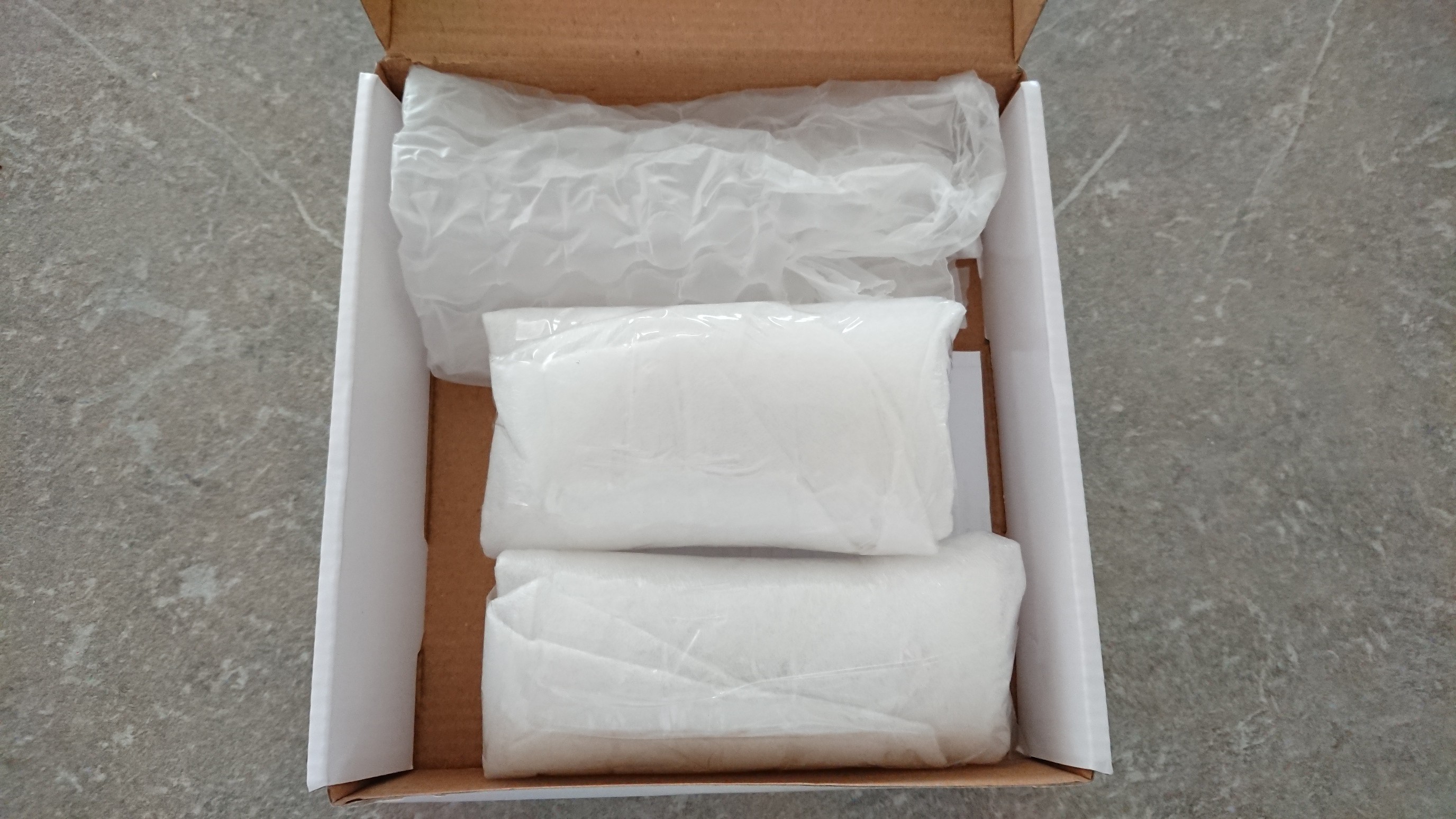
    The package came pretty quickly (FedEx, "IOSS" whatever that means) and the parts were very well packaged inside:

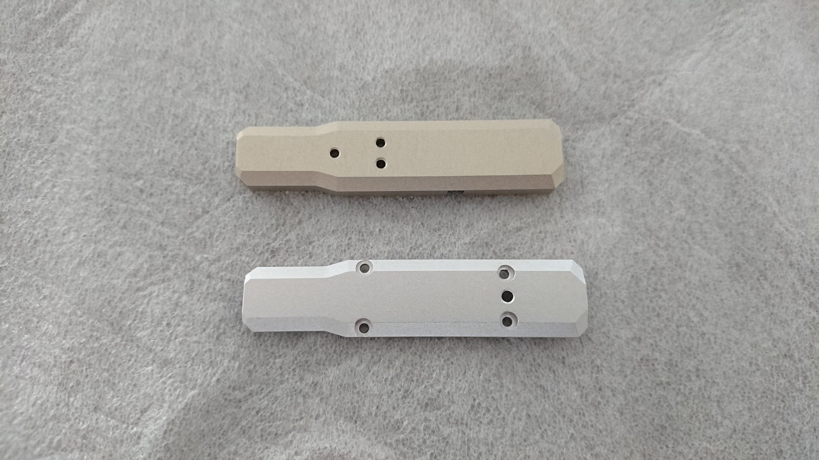
    Nice! Let's take all that wrap off:

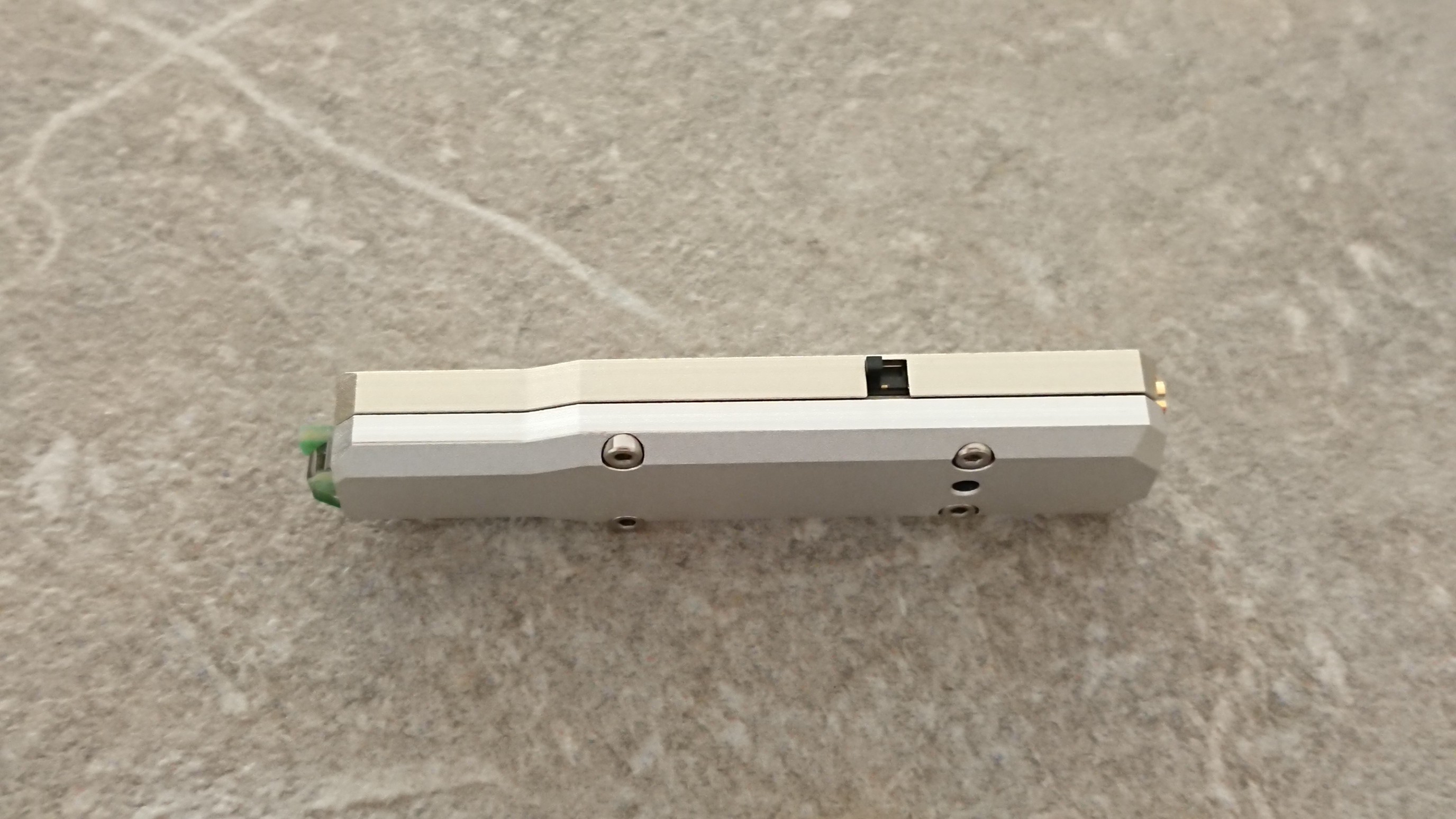
    Gorgeous! Not a single scratch or dent, and the parts have a smooth, silky feel to them. The top part is gold anodized and the bottom is natural. They fit perfectly:

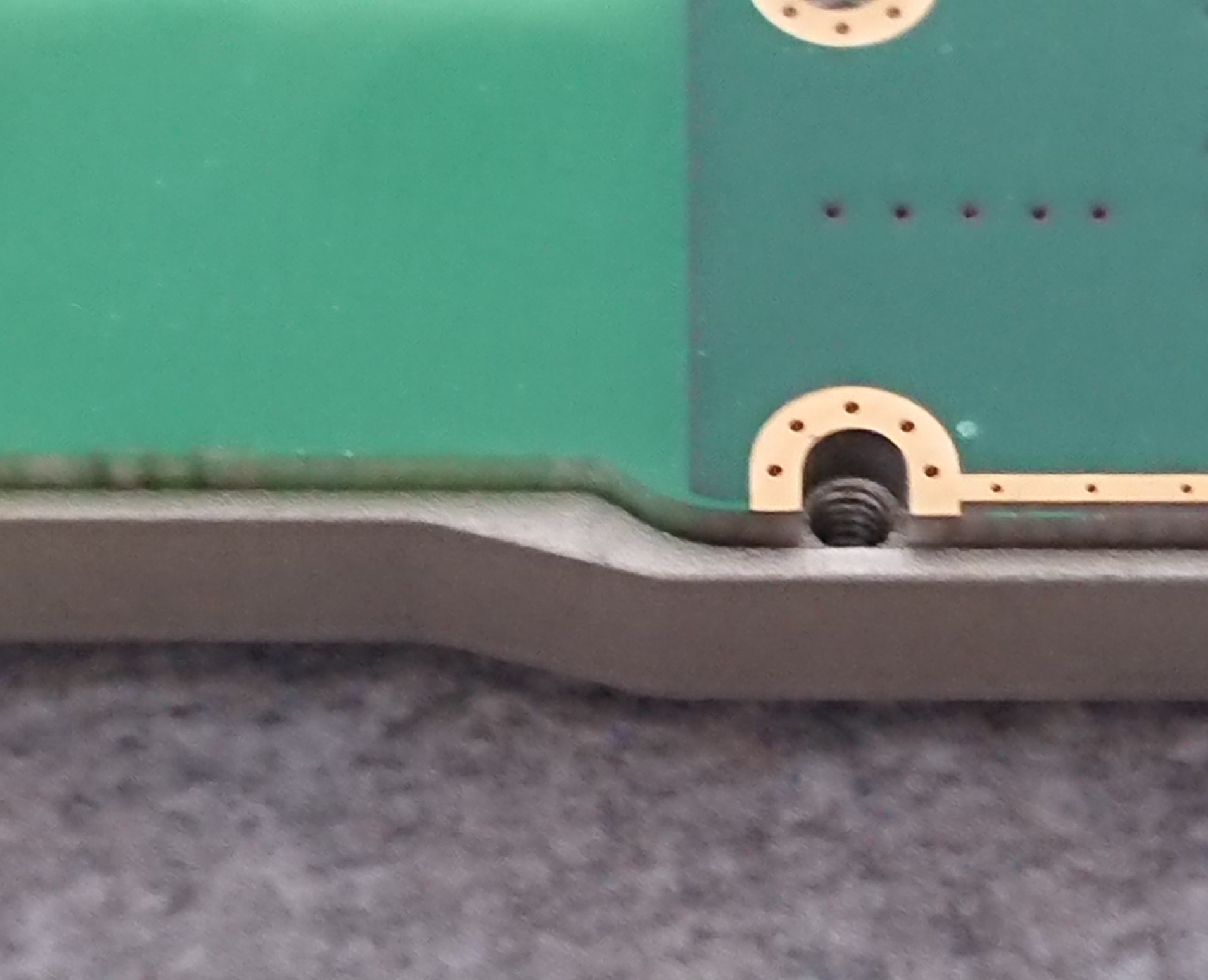
    Those M2 screws need an internal thread in a blind hole. I had previously cut some of these in desktop milled parts, and that was no pleasure. The threads from PCBWay were pretty good:

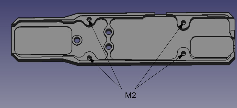
    To get those I had to supply a "drawing", as noted above. My drawing was pretty minimal, because I couldn't create a decent professional looking technical drawing myself. Instead, they got this:

    That was apparently sufficient, I got no questions back and they cut the threads to 2 mm usable depth, which was absolutely enough for M2 and probably close to the maximum depth they could have cut in this part anyway.

    Overall, a very good outcome!

  • Design Files!

    Christoph04/19/2022 at 20:49 0 comments

    Repo for the initial version which was just an eyeballed copy of Wolfgang's design: https://github.com/crteensy/FETProbe_v0

    Repo for the "tiny" version with RF shield and power supply/signal through u.Fl: https://github.com/crteensy/FETProbe_tiny

    The build is pretty simple, but there are two things to point out:

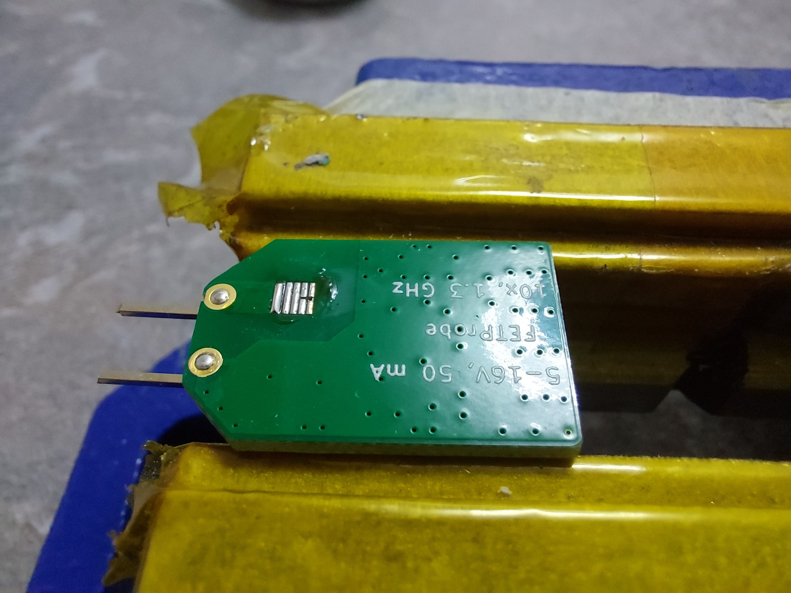
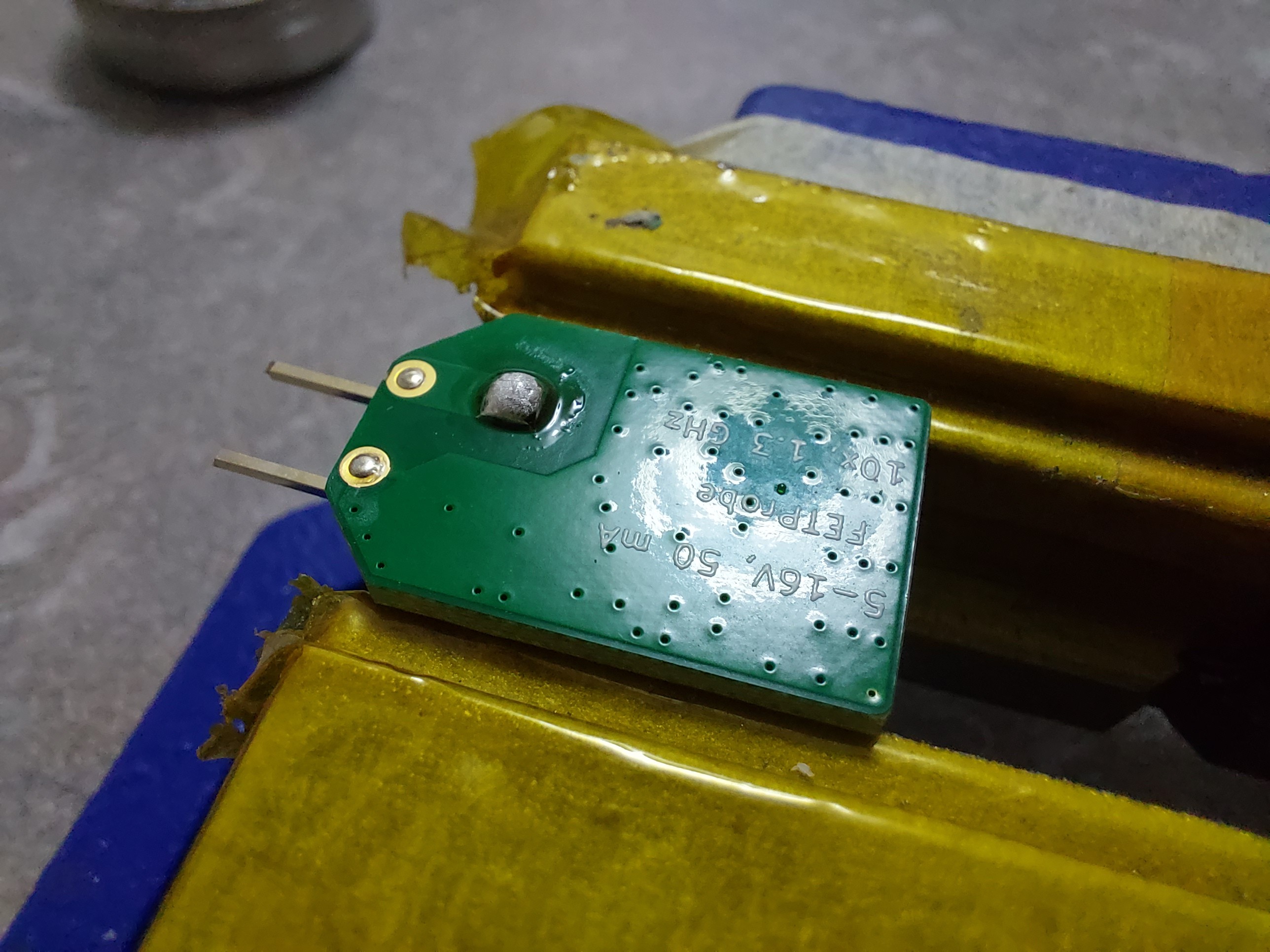
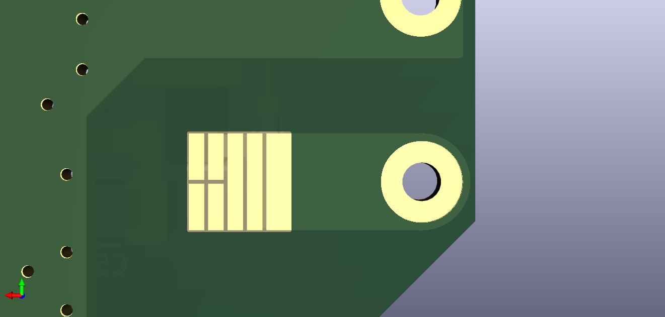
    The input capacitor is not a component you can pick up and place, but it's formed by copper features on the PCB. Here's the top part, a large pad next to the FET's gate 1 (pin 4):

    On the bottom we have copper as well, but connected to the through-hole input pad and configurable by some little extra copper pads:

    We haven't tried it but theoretically the probe can be tuned a bit with this.

    The second thing to note is that the RF shield must be modified prior to soldering, because it would otherwise provide too much stray capacitance and wouldn't really fit either. So one sidewall has to be removed:

    I did this by filing the edge off a bit and then wiggling it until it fell off entirely.

    However, before the shield can be soldered on, all the other parts have to be soldered. It's not much:

    I'm thinking about ways to make it smaller, but that would probably require a custom RF shield. And it works.

  • The beginning

    Christoph04/18/2022 at 22:22 1 comment

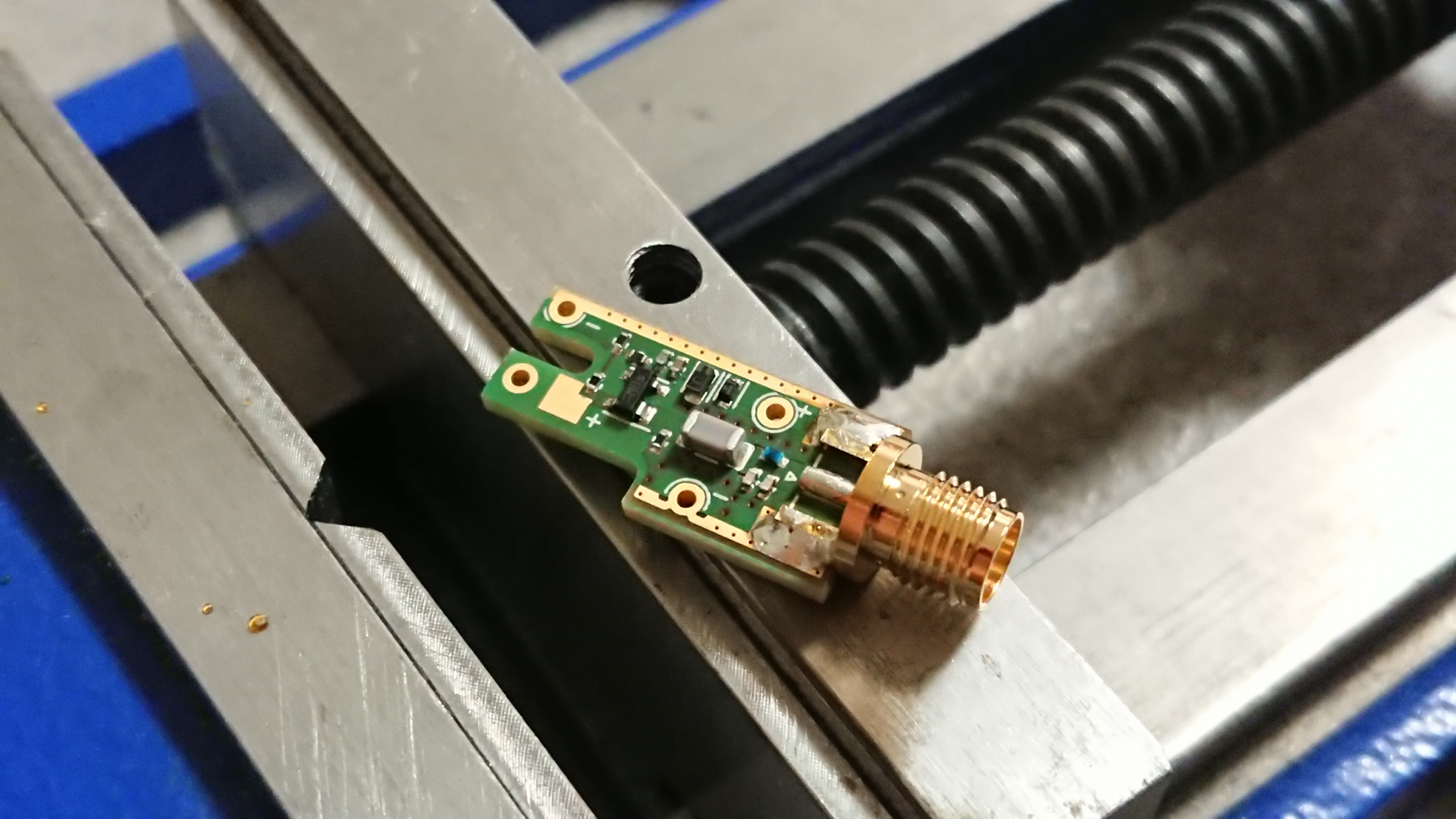
    Wolfgang designed his PCB in PCBExpress (I think), so I recreated his layout in KiCad. This was the result:

    This was pretty small already, but was quite inconvenient for a couple of reasons:

    • The power supply didn't have a connector, it was done through two soldered wires. That's not a problem per se, but the signal output is done through an SMA jack. It was only partially "pluggable".
    • Without an RF shield, touching the probe changes its output. That is indeed bad.

    I sent it to Wolfgang anyway, and it performed well. The next step was to improve the design a bit towards a tool that can be handled well, and that can be solderen into a circuit (for when lead inductance really counts). The SMA was swapped for a u.Fl, and so was the power supply input. Adding an RF shield wasn't so easy because the common, small, off-the-shelf parts all have four walls. I picked a small one that looked easy to modify, and came up with this:

    This is the probe characterized on Wolfgang's page:

    https://electronicprojectsforfun.wordpress.com/solder-in-probes/

    Next log will be about assembly and will also contain a link to a repo with layout files and all that.

View all 7 project logs

Enjoy this project?

Share

Discussions

Bud Bennett wrote 09/15/2022 at 22:25 point

Hi Christoph, This probe was designed to have a "low capacitance". What is the design goal? What is the measured input capacitance? I looked at the BF998 (an obsolete part), which specifies a Gg1ss = 2.1pF. But the capacitance that you care about is from gate to drain, which doesn't appear to be specified in the datasheet. Wolfgang did not measure it as part of his evaluation...

  Are you sure? yes | no

Christoph wrote 09/15/2022 at 22:31 point

Hi Bud, thanks for asking - I think the ones he built had 1.3 pF, but I don't remember the exact number he measured for my version. I'll ask him.

  Are you sure? yes | no

Christoph wrote 09/20/2022 at 21:22 point

Without pins attached, Wolfgang measured ca. 0.4 pF.

  Are you sure? yes | no

Similar Projects

Does this project spark your interest?

Become a member to follow this project and never miss any updates