 Alain d'Espaignet
-
1A simple circuit
To illustrate the concept I picked a simple LED flasher circuit based on the well known 555 timer integrated circuit.
I choose an LED flasher because when I do implement the idea I have a quick and visual way of telling if it is working.
Hey it either flashes or does not! It's a binary decision and as basic as it gets.
-
2I use the circuit described here:
-
3Theory
If you are interested in the theory of operation behind this circuit refer to the article link above.
For example you might want to use the design equations provided to make the LED flash at different rates.
The good news is with the 3D cavity plate packaging idea being presented here you can easily swap part values and see the effect immediately, no desoldering, re-soldering required!
-
4Parts selection
I made no particular effort in choosing the parts based on availability and or price as one would normally do in electronics design.
The purpose of this exercise is to illustrate how the idea fits in with the traditional electronics product design workflow.
I went with simple R1210 SMD packages for the resistors and capacitors because they are large enough to see and manipulate.
I had a hard time finding connectors for which there are existing 3D models in the available EAGLE libraries.
It seems no one is interested in creating 3D models for those.
It doesn't really matter when converting the PCB to 3D EAGLE/Fusion 360 will use a dummy 3D model for it.
The down side is unless I create a 3D model for it I wont get a realistic 3D representation of the PCB out of the box.
When it comes to “realizing” the circuit if I run into trouble with part availability and costs I’ll have to make adjustments.
-
5The software you’ll need
To reproduce this test circuit you’ll need the following:
Software
Cost
URL
Purpose
Autodesk EAGLE
Free
To design schematics and printed circuit boards
Autodesk Fusion 360
Free for personal use
To convert printed circuit board to 3D
To create 3D models of parts
To create a 3D cavity plate
CAD assistant*
Free
To view .step files quickly
* Optional
-
6Autodesk EAGLE
I used EAGLE to create the schematic.
The long standing EAGLE software product has been purchased by Autodesk and is now rebranded Autodesk EAGLE.
Autodesk took a tried and tested schematic and PCB solution and took it to new heights.
The workflow is the traditional simple workflow you most probably know, with some variations.
If you are an electronics hobbyist who dabbled with schematic and PCB programs there is no rocket science in the processes shown here. Anyone initiated to schematic and PCB and 3D modeling software usage can do this.
-
7Alternative software
There are lots of free software offerings for creating schematics and PCB nowadays.
I picked EAGLE because of its tight integration with Fusion 360 and the fact I checked that it lets me apply my process variation relatively easily.
In the past you had to use third party User Language Programs (UPL) in EAGLE to convert 2D PCB to 3D.
I remember Blender was used for the 3D rendering aspect.
With Fusion 360 this has all become very simple.
As an added bonus Fusion 360 leads to the possibilities of 3D parametric design, 3D printing and CNC milling.
There are other alternatives that you can explore on your own but this tool set will do the trick.
In principle you need the following core features:
- Ability to create your own 3D models for parts on a circuit board.
- Ability to perform boolean operations.
- Ability to 3D print or CNC mill.
You can use multiple programs to achieve the same goals however with Autodesk EAGLE/Fusion 360 integration you have a one stop solution for realizing every aspect of the idea being presented in this contest entry.
Note the process is not perfect due to some EAGLE/quirks but it could be made smoother with the assistance of AddIns.
I’ll get to that in the implementation part of the competition.
-
8Here is my schematic created in EAGLE:
![]()
-
9PCB
Creating a PCB from a schematic in EAGLE is easy: File → Switch to Board.
-
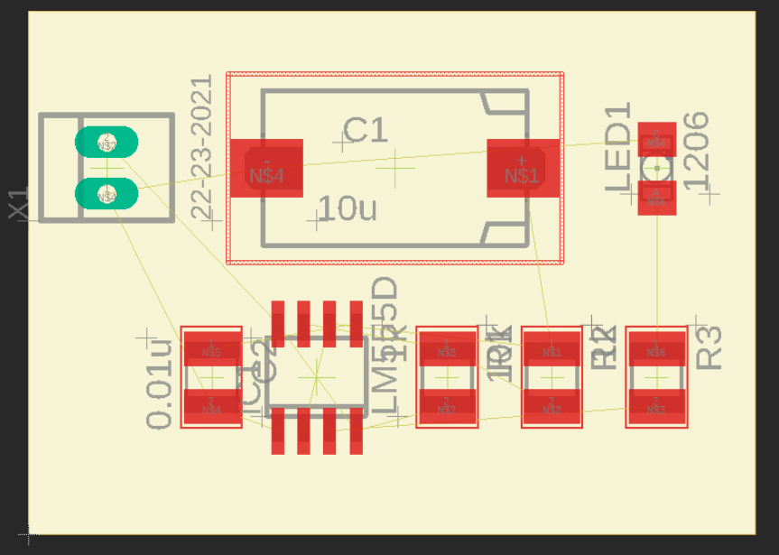
10Placement
The next step is the placement of the parts on the PCB.
I am not too interested in an optimal placement because my intent is to illustrate the general idea for this contest.
The only few things I will consider is that ultimately the parts on this PCB will be held in place by a cavity plate as I call it.
That cavity place can either be implemented using 3D printing or CNC milling.
Therefore I need to be aware of the limitations of these implementation techniques.
For example with 3D printing the boundaries between the cavities cannot be too thin or they might get deformed.
I am not trying to push the limit at this stage but only illustrating the core concepts so I’ll keep it simple and realizable.
Validate the idea, optimize later.
Here is my placement:
![]()


Discussions
Become a Hackaday.io Member
Create an account to leave a comment. Already have an account? Log In.