 Alain d'Espaignet
-
11Routing
There again I will simply use the EAGLE built in autorouter for I am not trying to make this PCB single sided or optimize in any way. The routing is as rude and crude as it gets with the placement I choose.
![]()
-
123D PCB
Now comes the fun parts creating a 3D PCB. With Fusion 360 integration with EAGLE that’s a matter of a few clicks.
This is not a 2D PCB to 3D tutorial refer to the many tutorials and videos for that on your own.
![]()
-
133D rendering
![]()
At this point we have a complete 3D PCB. We will use this as a reference for construction.
-
14Now the real work starts
The end goal is to create a “cavity plate” that mounts on top of the PCB and has cavities in it.
The parts mount inside the cavities.
This plate will hold the components in place and press their pins against their respective SMD pads to make an electrical connection.
To do this we create a plate with the same shape as the PCB but a little thicker than the highest part on the PCB.
From this place we will cut out using boolean operations the cavities for each part.
-
153D cavity models - SOIC8
Let’s consider the SOIC8 SMD package for the LM555.
![]()
As you can see from the data sheet there is a small clearance between the bottom body of the part and the bottom of the pins.
With pressure applied to the top of the part body there is a small amount of “springiness” that will help the chip pins make contact with the SMD pad landings on the PCB.
For good contact it is best to make a cavity that will have a small ridge over the pins to push them down on the PCB pads.
Here is what we want to achieve:
![]()
To do this we will create a 3D model that has this shape for the SOIC8:
![]()
The SOIC8 will fit in this “cavity” like this:
![]()
Then we subtract this cavity shape from the cavity plate using boolean operation:
![]()
We end up with this:
![]()
Now the chip will live inside this cavity in the plate. The plate will push its pins against the pads.
![]()
Here is a representation of this with the cavity shown as transparent:
![]()
I trust that you get the general idea. An inverse mold of the part is being “cut out” from a solid plate.
The same principle applies to all other parts.
So now the task is to create 3D models cavities for each part then recreate a 3D PCB with those instead of 3D models used for realistic visualization.
That’s a tedious task.
In the short term I will do this manually however in the long run the process should be assisted by software.
It can be implemented as a plugin for Fusion 360.
-
16Creating 3D models for cavities
Using Fusion 360 the process starts with exporting each 3D model from the 3D PCB to STEP format.
I will use these STEP files as a guide to create their “cavity” equivalents.
It is important to use a format that is not just a mesh, that is a set of vertices and edges.
Fusion 360 cannot perform boolean operations on meshes; it has to be “bodies”. STEP preserves bodies.
In the 3D PCB there are just a few part types.
![]()
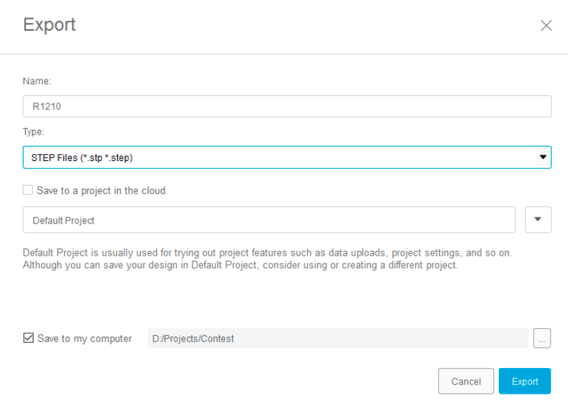
In Fusion 360 export then by selecting each different package type them in the “BROWSER” window right click and choose Export.
![]()
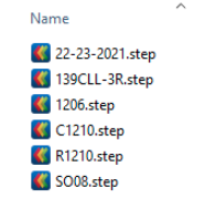
This process yields a set of STEP files:
![]()
They can be visualized using CAD Assistant.
![]()
-
17Fillets
3D models created for realistic visualization often have a lot of unnecessary details. Some also have rounded corners like for capacitors and resistors. These must be removed because you want sharp edges to make contact with the PCB so that when doing the cavity cut out boolean operation you don’t end up with those small fillets.
-
18Modeling cavities
Open each of the STEP files exported to use them as a guide for modeling cavities.
Considerations for cavities
The cavities must account for the package dimension variations. The max or average values from the dimensions given in the data sheet should be used but it also depends on the material used for the cavity plate.
It is not necessary to make the cavity 3D models go between pins or follow every detail of a part. In fact, considering the pitch on an SOIC8 part is 0.65 mm there would be a small gap between pads, probably too small to manufacture accurately using today’s 3D printing and or CNC methods.
I did this exercise years ago around 2008. I used an Objet 3D printer service offered at a startup at the University of Florida. At the time it had the highest resolution you could get on the market. In this trial run I made the mistake of faithfully reproducing cavities of the same shape as the IC’s. The details got lost. I also use the wrong material. I thought I’d use a material that had some springiness to it. I ended up with a cavity plate that feels like gummy bears! It would deform easily.
-
19Copy the project
The next step consists of making a copy of the EAGLE project and giving it a new name.
To do this create a new project giving it a new name. Originally the project was named 555. The copy I named 555-c.
Navigate to the location of the project files and copy the .sch and .brd files to the new project folder.
Rename the .sch and .brd file to the same name as the project i.e. 555-c.sch and 555-c.brd.
Open the schematic and make sure you can navigate to the PCB.
The reason for renaming is to preserve a copy of the 3D PCB in Fusion 360 and create a new one.
If you don't rename both the schematic and board when converting to 3D in Fusion will use the same name.
Also remove the link between the original EAGLE PCB and the prior Fusion project for you want to create a new one leaving the prior project intact.
All this is the extra gymnastics you have to do in EAGLE to achieve the end goal. These steps should be automated with software.
-
20Replacing 3D models with cavity 3D models
In this step we replace the original realistic 3D models with their cavity equivalents so that we can later cut them from the cavity plate.
In the EAGLE → Fusion 360 tool chain there are multiple ways of replacing 3D models.
An easy way is to do it in the Schematic Design Manager in the schematic.
In the schematic 555-c.sch I replace each part one by one by selecting it and choosing:
![]()
The Package Editor dialog comes up. From its menu select Add Custom 3D Package and select the .STEP file created for the cavity for the package.
This step is tedious. This can be streamlined through EAGLE ULP/Scripts in future.


Discussions
Become a Hackaday.io Member
Create an account to leave a comment. Already have an account? Log In.