Ricardo Tonet
-
It's alive!
07/23/2022 at 00:42 • 0 commentsI've been working slowly on the firmware side, although free time is becoming a rare commodity on my side.
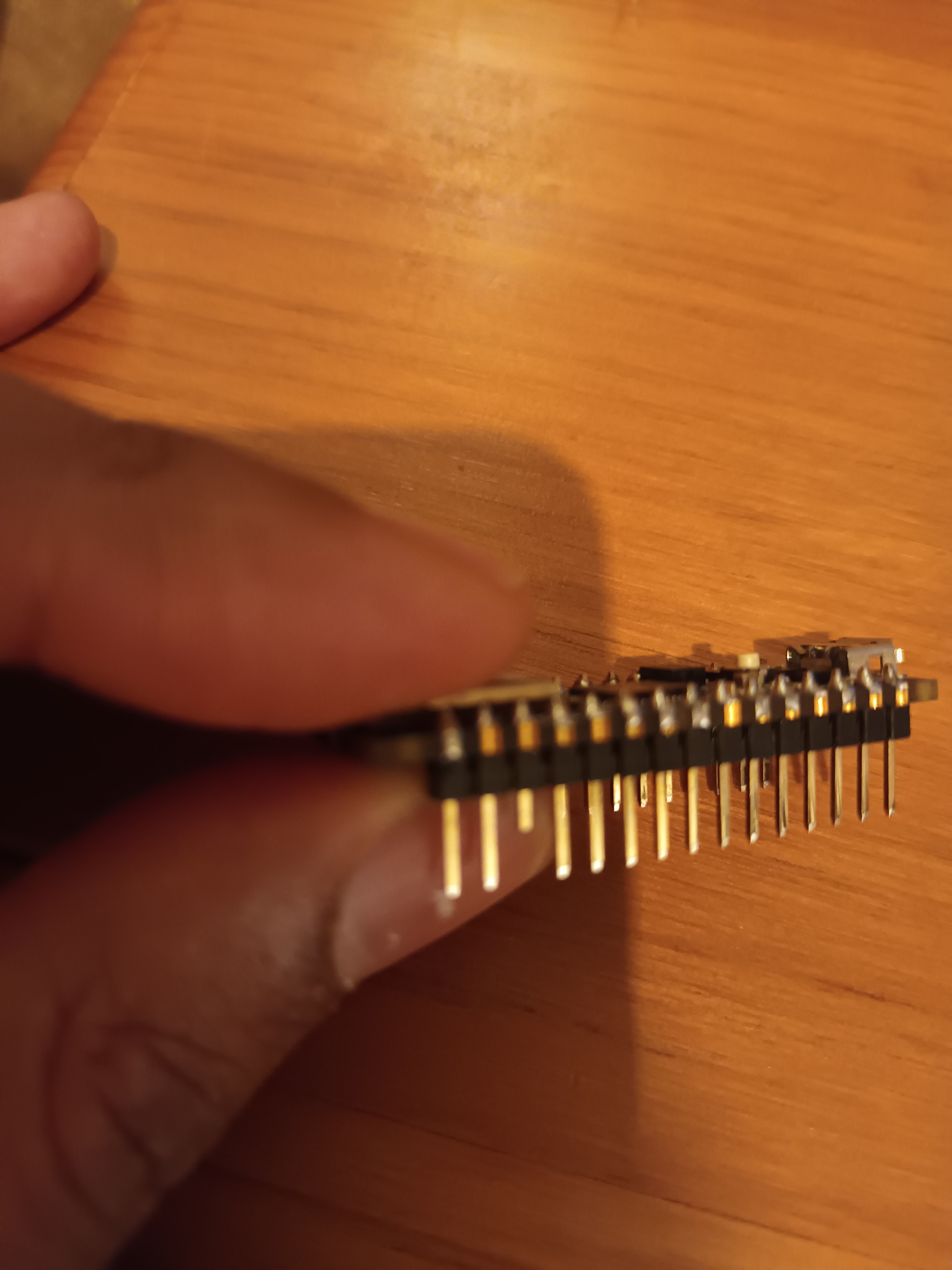
While starting the firmware development I noticed a few more schematic and PCB mistakes. One of them was major. During schematic I misplaced one position in a few Arduino socket pins. I ended up connecting the GND plane to the Reset pin instead of the GND pin. This left the Arduino on reset. I had to cut the Arduino reset header pin to prevent it to touch the socket. I also had to shunt two socket pins, and break the buzzer lane and connect it to the right pin with a wire to the PCB bottom.
![]()
![]()
![]()
The other mistake was again a footprint inversion. I ended up flipping the buzzer polarity. It does not seem to work at the moment, probably it is broken. Have to do a little more debug on that. Definitely, there must be a PCB version 1.1.
Besides this, everything else so far seems to be working fine. I only haven't tested the screen and rotary encoder.
At the moment, I've already done the LDR, LED, MIC and DHT20 drivers. I can read their values and print on the serial console. The LEDs can also turn on/off, blink at chosen frequencies and fade in/out. For the LDR and MIC I tried to calculate the LUX and sound intensity in absolute dB, but the values are not correct. For the LUX I tried a quick calibration using a mobile phone lux meter app, but I need more points to find the right calibration curve. For the sound intensity I used the mic datasheet data and a few equations for the conversion but something is off. I will fix it later.
Right now, Suricata is ALIVE!!!
-
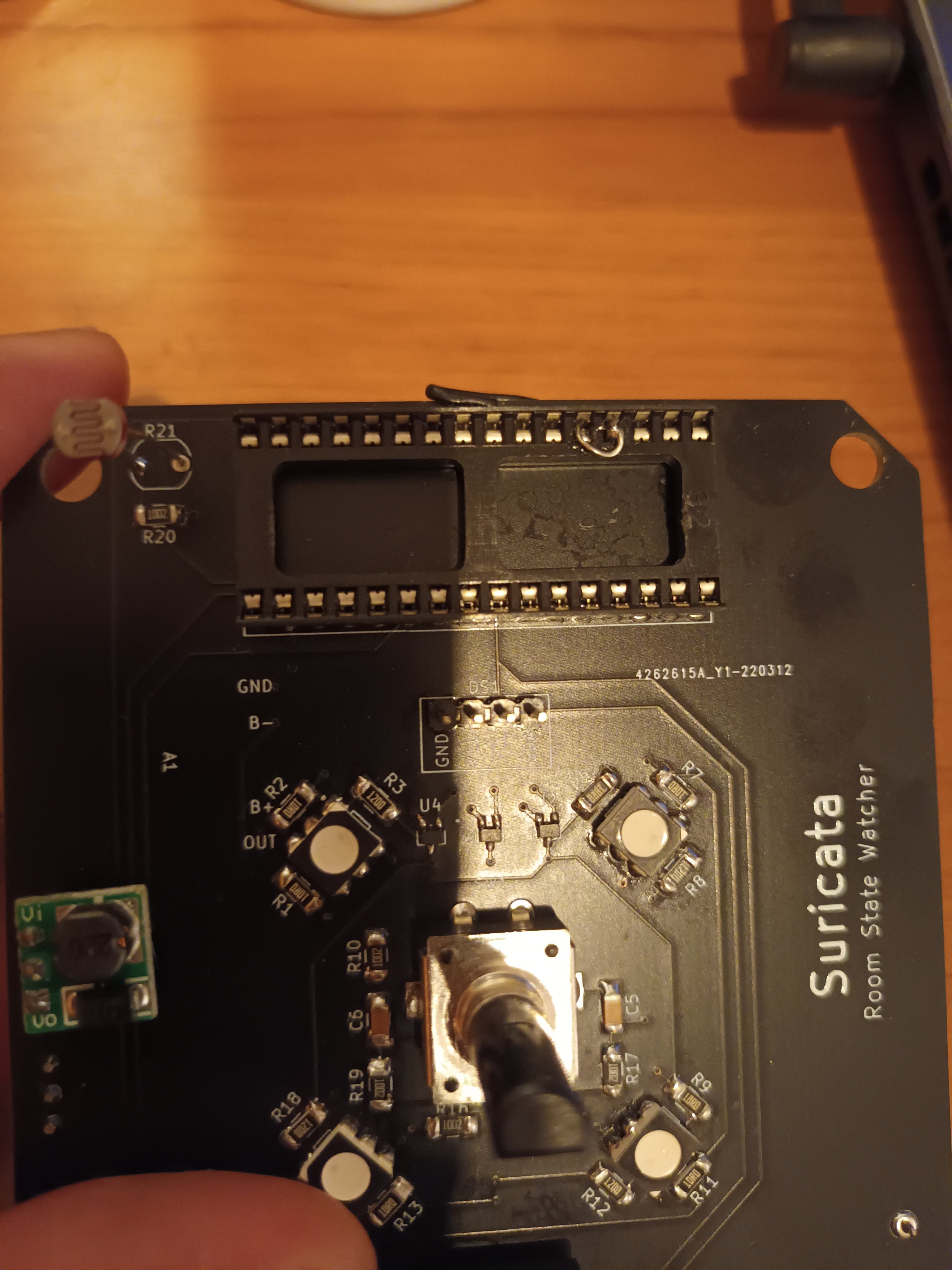
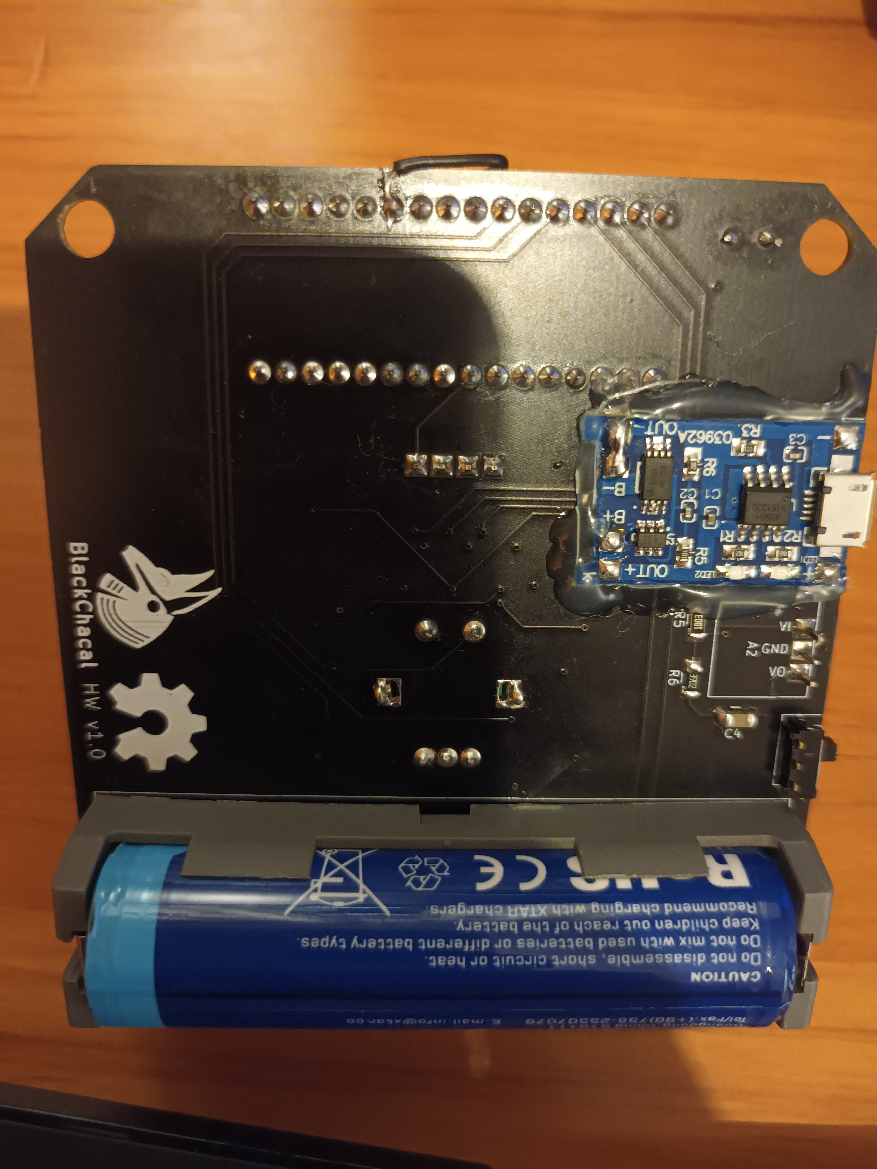
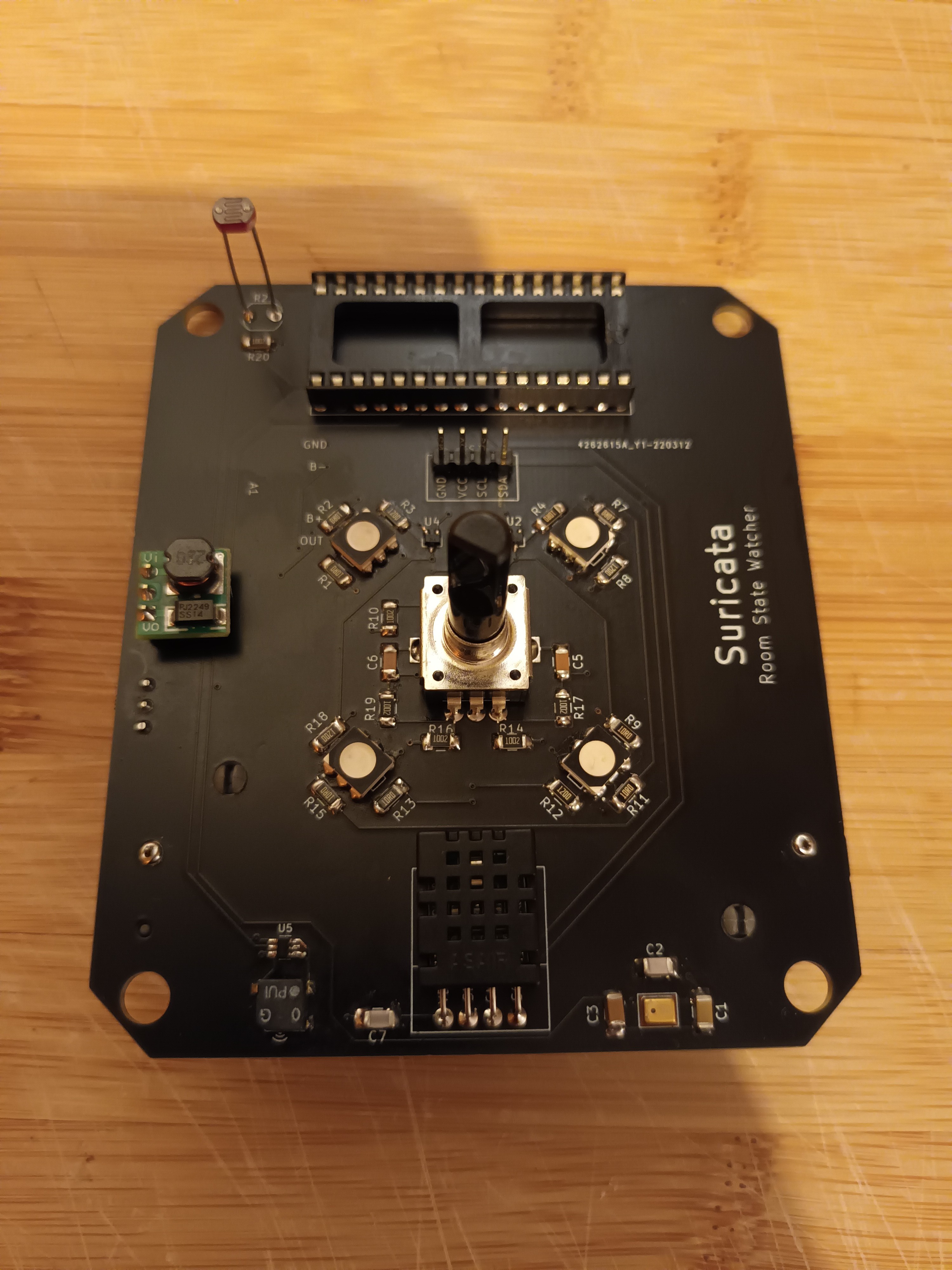
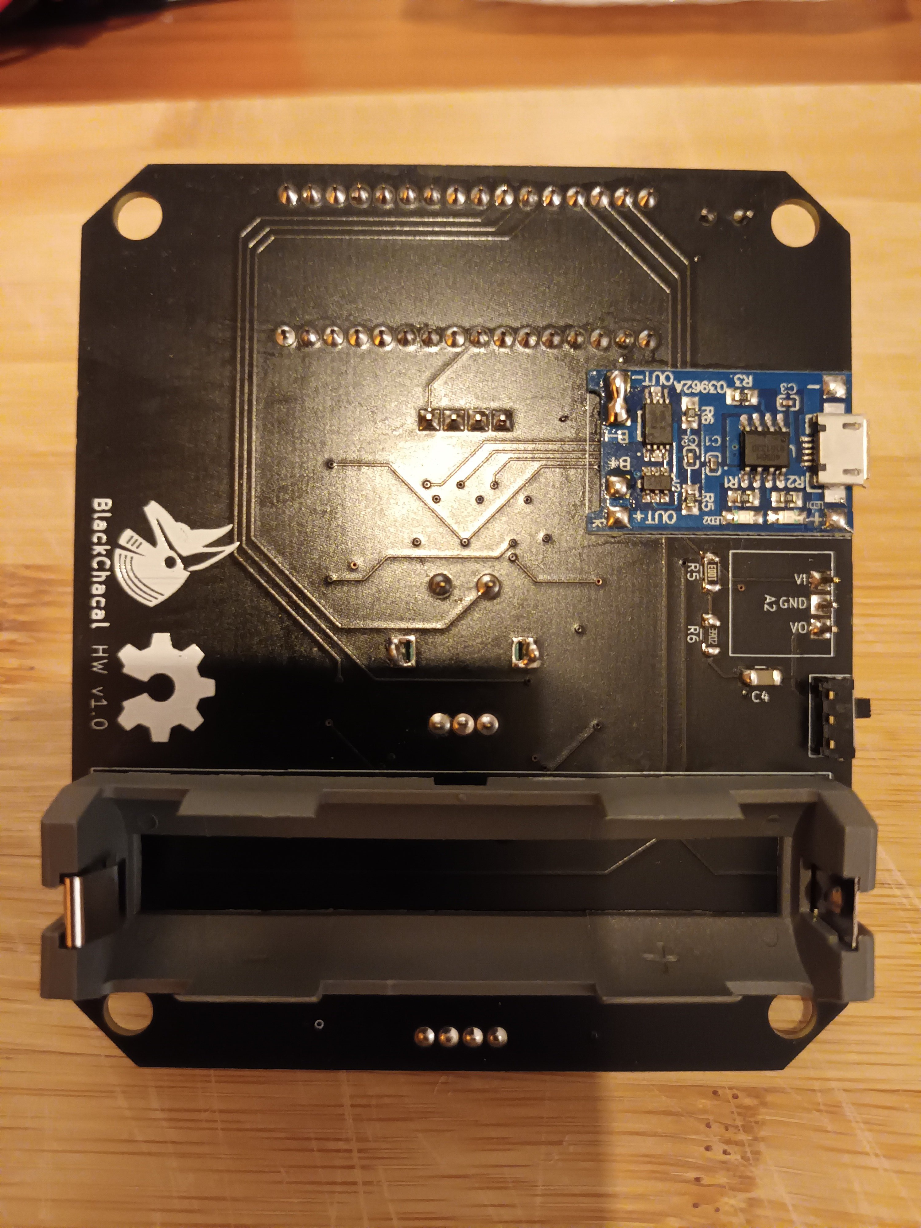
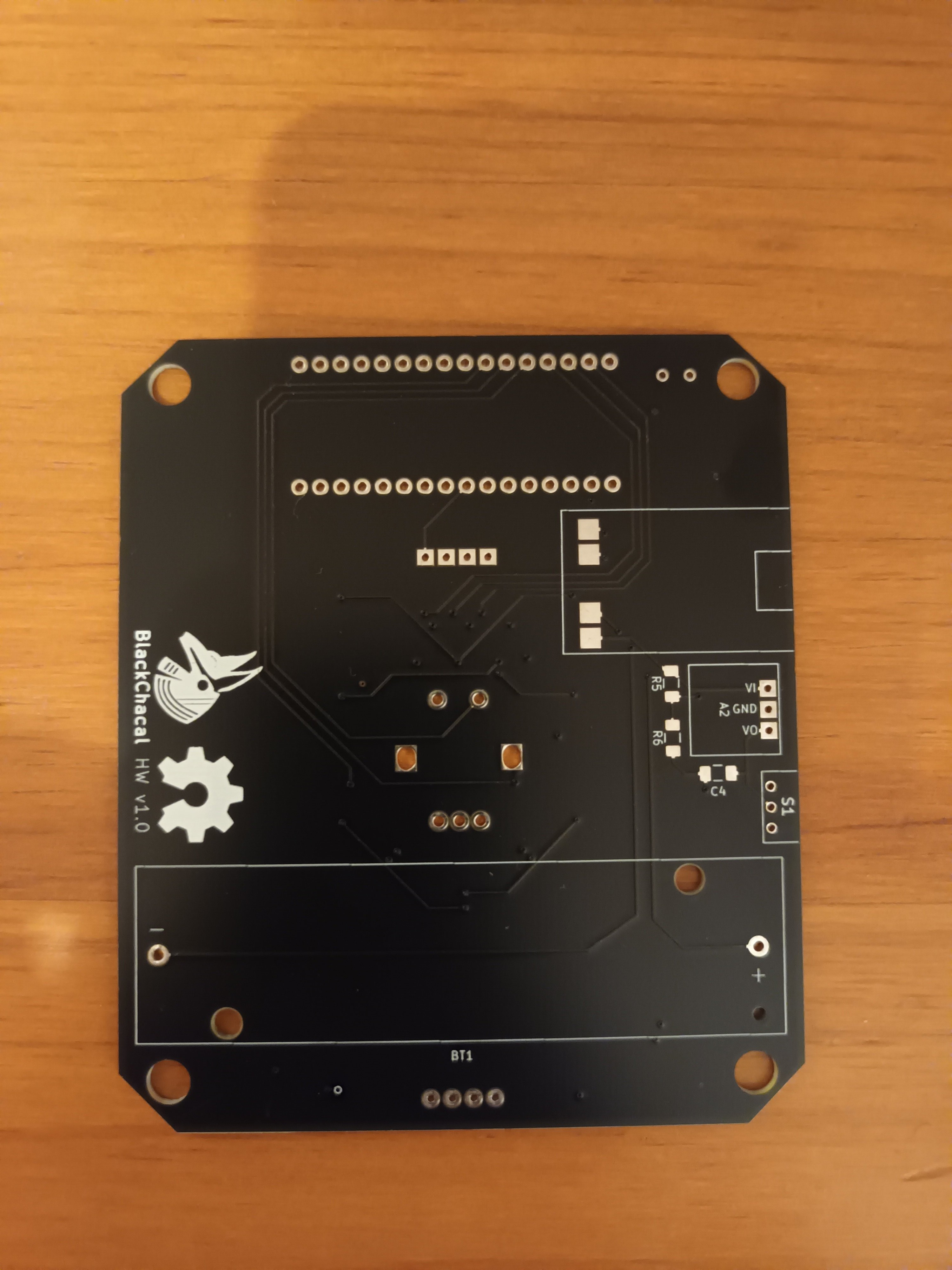
PCB Assembled
06/09/2022 at 01:39 • 0 commentsFinally I have my PCB assembled. I took me a while because I was assembling 5 PCBs at the same time, although, only one is complete. I did not buy all the components for the five of them. I will later on.
During assembly I also noticed a few mistakes on the PCB. The component A2 is a boost step up breakout board to 5V. I switched the Vin and Vout pins on the back footprint, so I had to solder the component in the front.
The component A1 is a LiOn battery charger breakout board. I forgot to connect the GND to the battery (-) connector on the schematic and PCB. I ended up making a solder bridge between the two pads directly on the breakout board. I tested the Power supply and it seems fine. This component also has the pad description footprint showing on the front instead of the back.
I already started the final fw with arduino on the breadboard. After fully testing the board I will start to develop directly on the PCB.
Here are the assembled PCB pictures:
![]()
![]()
-
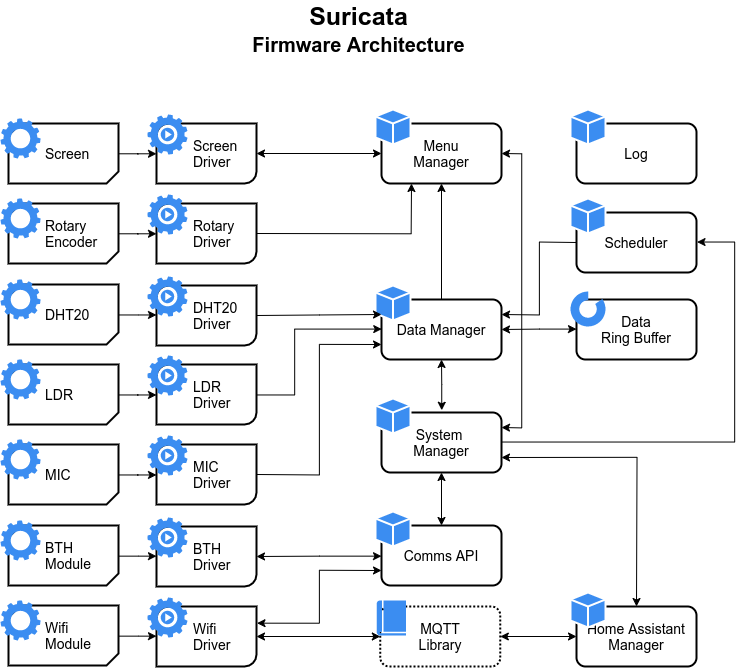
Firmware Architecture
05/24/2022 at 01:02 • 0 commentsDefined the firmware architecture to start implementing soon.
![]()
-
Current Status
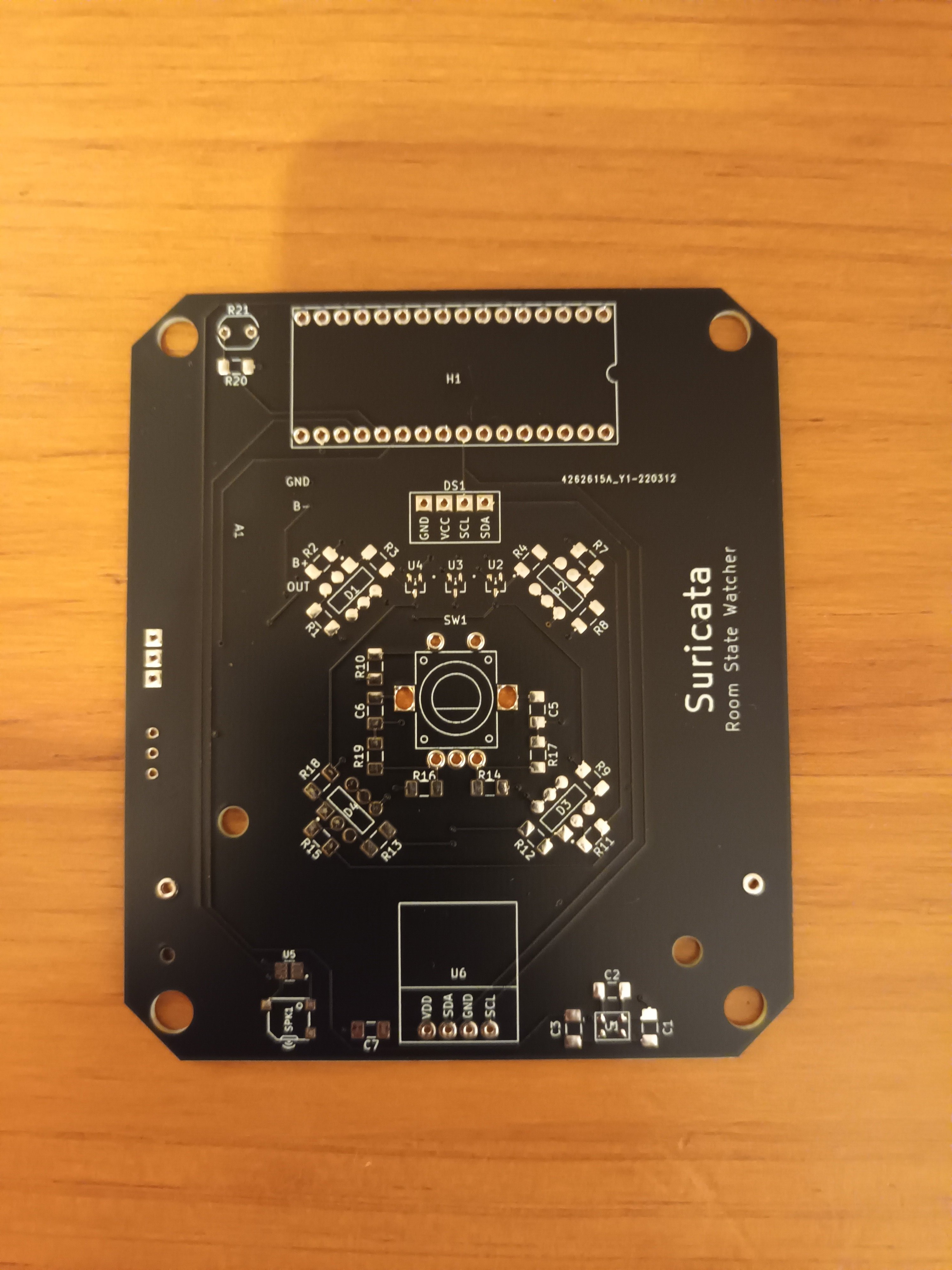
05/22/2022 at 02:12 • 0 commentsAt the present moment, the first prototype already has the PCB manufactured at JLCPCB.
![]()
![]()
The components were also purchased and the soldering will start soon.
The firmware development will also start soon, first on the breadboard setup, and later on the final hardware, once assembled.
Suricata
Wireless indoor environment station that monitors temperature, humidity, light intensity, sound intensity and gases.