zpekic
-
Internal CPU extensions
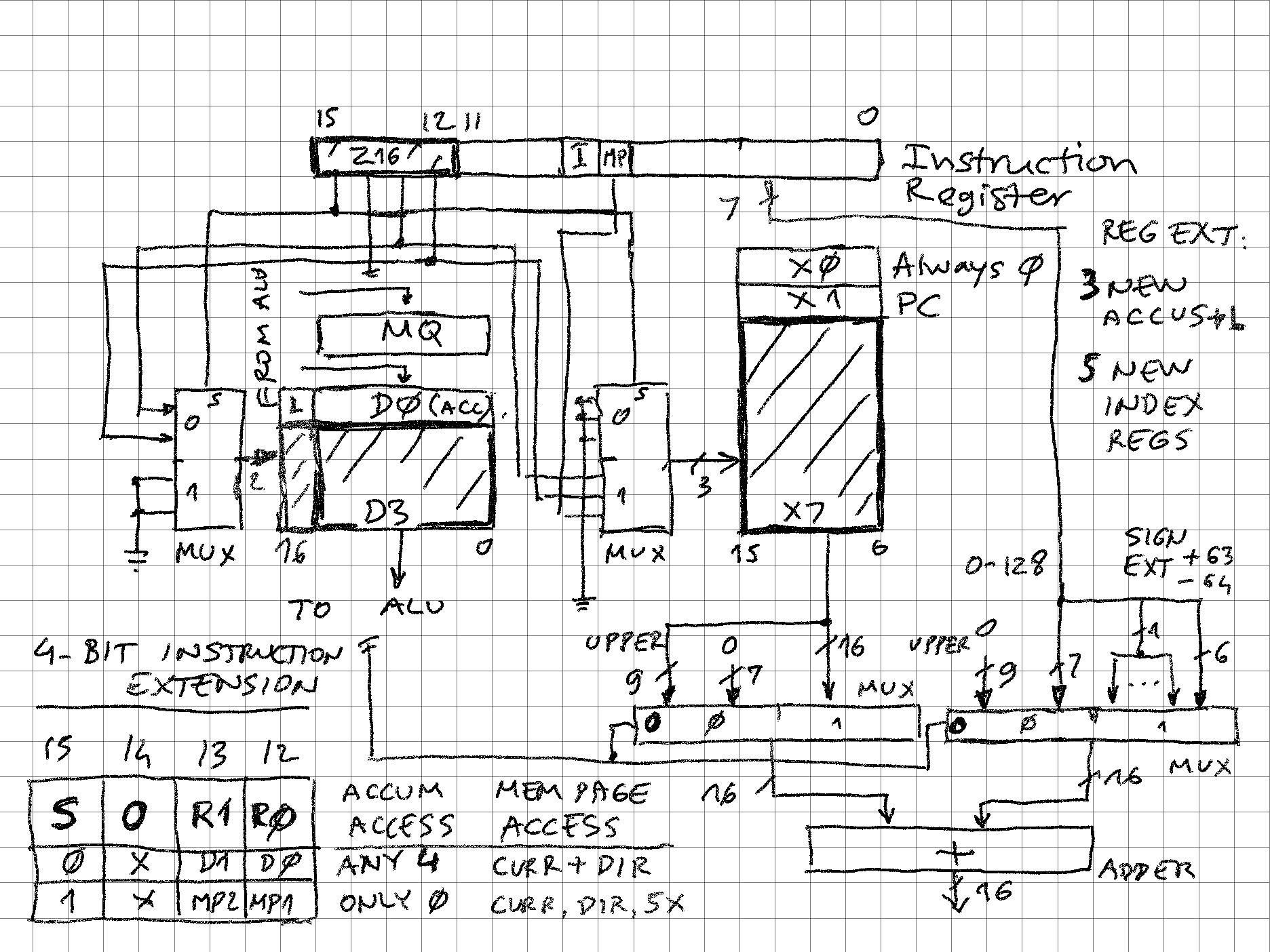
06/12/2022 at 02:31 • 0 commentsThe schema below illustrates the additions to CPU programming model and how they are activated by the upper 4 bits of the instruction register. Some notes:
- Microcode (or state machine) driving the instruction execution has no knowledge of the registers being used - it will use ACC/L or PC, or any X (index register) as the selection happens by pointing to 1 out of 4 or 1 out of 8 purely in hardware
- ACC/L mux - based on IR15 (S), either ACC/L(0) will be selected, or any of 4 given by IR13:12
- Once ACC/L is selected, rest of hardware (mostly ALU) sees 1 ACC/L exactly like in the legacy PDP-8
- X mux - based on IR15 (S), selection is either 0:0:MP or X2:X1:MP - because direct page register is mapped to X0 and PC to X1, changing S bit on the fly from one instruction to another does not disrupt the program flow
- X0 and X1 (zero, PC) are modified directly by microcode, so a bypass / force needs to be implemented on X mux but for simplicity is not shown below
- X0 can be used at T (temporary) register - as long as during memory address calculation for memory reference instructions is set to 0. Typically, a microinstruction step would clear it to 0 before instruction execution phase
- For memory reference instructions, first step is to evaluate the X + offset. IR14 (O) bit allows two ways to evaluate this - either "legacy" page|offset concatenation or real 2's complement addition. 2 muxs handle this - one taking X register value and the other the offset from IR
![]()
-
System "compatibility" schema
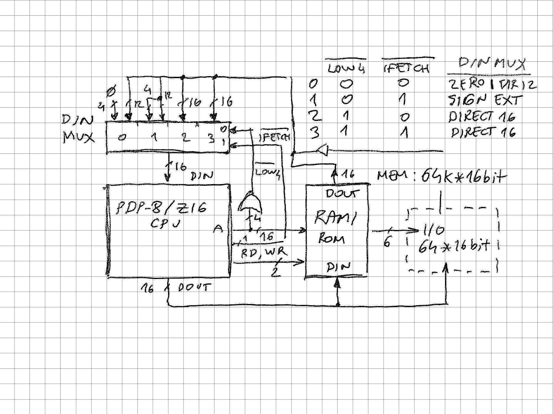
06/12/2022 at 02:16 • 0 commentsThe picture illustrates a simple way to force a PDP-8/Z16 system into "compatible" mode. As this is a theoretical/or maybe FPGA implementation, system bus can be designed in non-multiplexed way, with DIN (data in) and DOUT (data out) buses separated.
Some notes about the schematic below:
- DIN mux is supposed to feed instructions and data into CPU seamlessly if accessing "extended flat memory" (above 4k word), and if accessing PDP-8 basic 4k words, differentiate between instructions (force upper 4 bits to 0000 for "compatibility") and data (assume 2's complement so extent bit 11 to 12..15)
- DOUT goes directly as 16 bit to I/O and memory
- I/O can - based on actual device - be hooked up to any part of the 16-bit data bus, for example 8-bit devices could work on D7:0 or D15:8 etc.
![]()
PDP-8/Z16 - seamless extension from 12 to 16 bits?
PDP-8 has been studied for 50+ years due to the elegant simplicity of its CPU design - so why not ruin that with 16 bits? :-)