zpekic
Some key parameters of the proposed extension design:
- Internal registers extended from 12 to 16 bits
- Programming model extended to contain:
- 4 accumulators (each with own L(ink) flip-flop)
- 8 index registers
- 1 of 4 accumulators and its Link are the present in classic PDP-8
- 2 of 8 index registers are present in classic PDP-8: PC (program counter) and zero page (it can be represented as index register with hard-coded value of 0)
- Microcode driving the design is agnostic if CPU is running with basic or extended register set
- Some of the index registers can possibly mimic HD-6120 "stack pointers" in future versions
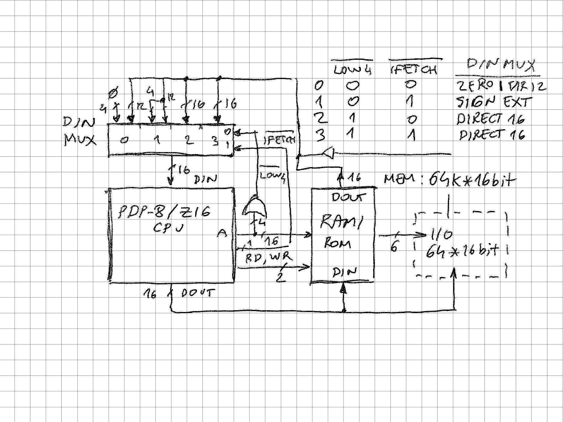
- Simple external circuit could force the CPU into "compatible" mode:
- If fetching instructions from lowest 4k of memory, force instruction upper 4 bits to 0
- If fetching data from lowest 4k of memory, extend bit 11 to 12..15 (seamless 2's complement representation)
- "Compatible" mode will fail in following cases:
- 6-bit characters etc. swap "bytes" is now swapping 8-bit halves, not 6
- counting bits in word, assuming there are 12 not 16
- possibly bit-masks assuming 12 entries or similar
- Needs verification, but most "simple" code should run with no or minimal modification in 16-bit mode too.
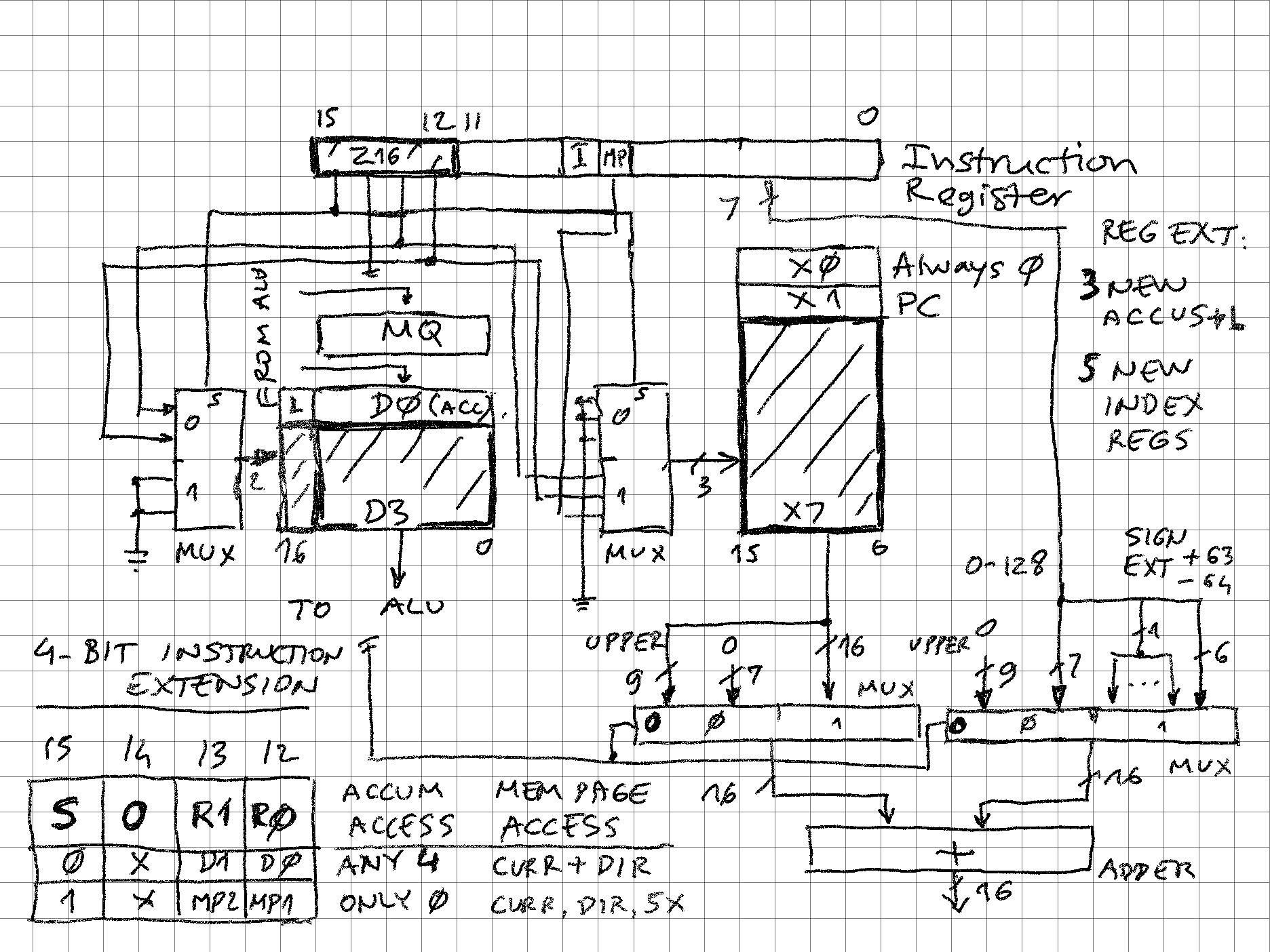
Instruction register is extended with 4 bits, 3 fields:
- S (bit 15) - select register mode bit
- if 0, field R1:0 represents extension of MP bit in the instruction for a total of 3 bits:
- 000 - zero page (X0 always contains 0)
- 001 - PC
- 010 - X2
- ...
- 111 - X7
- if 1, field R1:0 selects any of 4 accumulator/link pairs:
- 00 - standard PDP-8 acc/link
- 01 - acc/link 1
- ...
- 11 - acc/link 3
- if 0, field R1:0 represents extension of MP bit in the instruction for a total of 3 bits:
- O (bit 14) - address offset mode
- if 0, memory reference instructions calculate address by concatenating lowest 7 bits of IR with upper 9 bits of index register (same as usual PDP-8, so offset is 0 .. 127)
- if 1, memory reference instructions calculate address by real 2's complement offset addition: index register value - 64 to index register value + 63
- R1 (bit 13) - register select bit 1 (MSB)
- R0 (bit 12) - register select bit 0
| IR15 | IR14 | IR13 | IR12 | IR11-9 | IR11-9 | IR11-9 |
| S | O | R1 | R0 | 000-101 (MEMORY REFERENCE) | 110 (IOT) | 111 (OPR) |
| 0 | 0 | 0 | 0 | "compatible mode", just with 16-bit regs (00 - selects acc/link 0 and direct/PC reg) | compat mode | compat mode |
| 0 | 0 | X2 | X1 | 6 additional index regs can be used, with 0..127 offsets | compat mode | compat mode |
| 0 | 1 | X2 | X1 | 6 additional index regs can be used, with -64 .. +63 offsets | compat mode | compat mode |
| 1 | 0 | A1 | A0 | any of 4 acc/links can be used with direct or PC-rel addressing, offsets 0..127 | I/O transfer on any acc/link | operation on any acc/link |
| 1 | 1 | A1 | A0 | any of 4 acc/links can be used with direct of PC-rel addressing, offsets -64..+63 | I/O transfer on any acc/link | operation on any acc/link |
Loading / saving index registers 0..7: using reserved IOT instruction (each index register having own IOT address), regardless of the IR bits 15..12 - note that this means mapping PC and direct (zero page) register into I/O space too for simplicity of implementation.
Loading / saving acc/links 0..3: with IR bits 1XXX any can be accessed in any instruction format. Given that there is still just 1 MQ register in the design, it can be used in OPR to communicate between accumulators.
 Reed Foster
 Ed S
Ed S