# 2022-09-14 Keyboard
This board holds 99 keys total, spread out across a qwerty layout (64 keys), a "function key" row (14 keys), and a combined numeric/navigation block (21 keys).


|
Sidebar: Oh yeah, this one's a bit out of chronological order. I don't know why I started on the main board before being done with all three input boards. Eh, just blame my adhd. Anywho, here's filling in the gap. After this, I should be able to hook the ribbon cable up to a Raspberry and address most of the keys; I'll then continue with the VFD section, the trackball and the jog wheel. |
On the other boards, the switch casings themselves are merely soldered to the boards; they are not mounted onto a panel. Here, though, the key switches are mounted onto a separate 2mm steel plate which is screwed in place covering the large enclosure cut-out, making this board by itself weigh more than 1.25kg. This is obviously great for stability, but also prevents access to the front-side traces unless I either desolder all the switches from the board, or unclip all the switch casings from the plate, neither of which I'm going to do.
Arbitrarily numbering things:
- keyboard
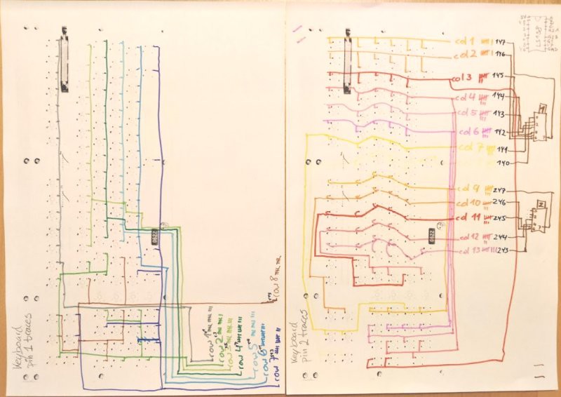
- ugh, mapping these turned out to be a bit of a mess. Rather than describing them here, I'm providing separate files with some colourful schematics as well as a spreadsheet of the complete key matrix.
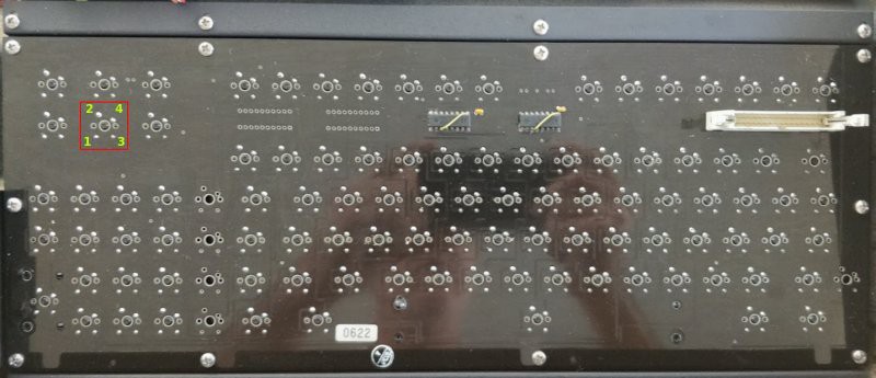
- key switches (red frame in above image):
- pin 1 is connected across the whole column-ish
- pin 2 is connected across the whole row-ish
- pin 3+4 are shorted to pin 2 when the switch is pressed
- between pins 1 and 2, there is a diode within the switch casing
- demultiplexers
- demultiplexer 1 and 2, with the one closest to the ribbon cable being chip 1
- ribbon cable
- standard numbering; pin 1 is closest to [3] and pin 34 is closest to [VIEW]
This board also uses the same demultiplexer select lines (23, 25, and 27) as the other boards.
On this board, pins 1 and 2 are switched around compared to the others: here, pin 2 on the key switches are run directly to the ribbon cable, and pin 1 on the key switches are run through a demultiplexer. However, the large number of keys on this board exceeds the capacity of a single chip, so there are two of them. About 2/3rds of the keys are run through demultiplexer 1, with the remainder being run through demultiplexer 2.
As usual, G1 is pulled high and G2B is pulled low, but each demultiplexer has its G2A pin is routed to separate ribbon lines: demultiplexer 1 uses ribbon line 21, and should be pulled low when scanning; demultiplexer 2 uses ribbon line 23, and should be pulled low when scanning. Note that ribbon line 23 is shared with the jog board (effectively placing a third of the keyboard keys on the jog board).
Curiously, the demultiplexer chips have no manufacturer or type printed on them, but are simply stamped with "Malaysia" and what is probably a serial number ("02M4" and "02G9"). I'm assuming they are compatible with the `SN74LS138` found on the other boards. Also, they're mounted upside-down on the underside of the board; the square solder pad is actually pin 8.
I've mapped the matrix in this shockingly artful diagram:

So in short, here is my new knowledge about the ribbon cable:
|
Ribbon line |
Source |
Signal |
|
19 |
Main board |
Keyboard board G2A chip 2 |
| 21 | Main board | Keyboard board G2A chip 1 |
Omitted: all of the bloody keys?! Well yeah, but they're listed in the spreadsheet file with the complete keyboard matrix.
 noughtnaut
Discussions
Become a Hackaday.io Member
Create an account to leave a comment. Already have an account? Log In.