Close
0%
0%

Iskra EMZ1001A - a virtual resurrection

4-bits wonder to print "Hello World!" and to calculate Fibonacci numbers to 13 decimal digits!

Public Chat
Similar projects worth following
Iskra EMZ1001A was the only microcontroller / microprocessor designed and produced in Ex-Yugoslavia (there are rumors CDP1802 was produced in Ei Nis, but I could not confirm). It was a collaborative design with AMI, and in rest of the world the chip was known as AMI S2000. However, EMZ1001A was not a copy, but truly a result of joint design, and chips were actually made in Iskra's factory in Slovenia.

(background photo: scan from article "Poluvodici", Tehnicka Enciklopedija, JLZ Miroslav Krleza, #10, V. Radic, R. Rocak - will remove if violating any copyrights)

Demo video: Mercury FPGA board running a virtual EMZ1001A based system, which displays "Hello World" and Fibonacci sequence to VGA, UART and 7-segment LED

The development of this project is mostly done now, and the code posted on github is fairly stable and complete.

In upcoming weeks my focus will be on documenting the most interesting aspects of the design. 

UPDATE 2022-12-16: Finished "System description" log entry

UPDATE 2022-12-18: Finished "Recreating a simple EMZ1001A assembler" log entry and uploaded demo video to YouTube

UPDATE 2022-12-19: Finished "Test code: Fibonacci sequence generator" log entry

UPDATE 2022-12-20: Finished "Test code: HELLo WorLd!" log entry (and updated previous one)

UPDATE 2022-12-26: Added "Running it on BaSys2 FPGA board" log entry

UPDATE 2022-12-26: Rewrote "Implementation in VHDL - instruction decode and control signals" log entry 

UPDATE 2022-12-27: Added "Implementation in VHDL: RAM and lookup tables" log entry

sys_emz1001_basys2.bit

Binary file that should work on BaSys2 FPGA board

bit - 71.07 kB - 12/26/2022 at 11:44

Download

sys_emz1001_mercury.bit

Binary file that should work with Mercury + Baseboard

bit - 146.11 kB - 12/19/2022 at 06:07

Download

  • 1 × https://www.micro-nova.com/mercury Mercury FPGA board
  • 1 × https://www.micro-nova.com/mercury-baseboard Mercury base board
  • 1 × https://digilent.com/reference/_media/pmod:pmod:pmodusbuart_rm.pdf PMOD USB to UART

  • EMZ1001 hardware tester available!

    zpekic10/02/2024 at 16:53 3 comments

    I don't know much about this project (I have problems logging into the website and interact with translated simplified Chinese), but it is super cool and wanted to share here:

    https://www.bilibili.com/video/BV1pC41137cS/?spm_id_from=333.999.0.0&vd_source=7d90cd143cf9e1646f422365630d6705


  • Implementation in VHDL - RAM and lookup tables

    zpekic12/27/2022 at 22:00 0 comments

    RAM

    All EMZ1001A RAM is implemented on chip, as 64 nibbles, arranged as 4 * 16 matrix, addressed by 2 bit BU (mr_bu) and 4-bit BL (mr_bl) registers. There is really no provision for external RAM, although possibly it could be implemented by INP and OUT instructions combined with manipulation of A lines, but it would be very inefficient. 

    RAM is implemented as 2-port read, 1 port write:

    • System read is always RAM[BU, BL]
    -- RAM is pointed by BU and BL
    ram_addr <= mr_bu & mr_bl;
    ram <= mr_ram(to_integer(unsigned(ram_addr)));
    •  Debug read is always RAM[dbg_sel]
      -- select debug outputs (RAM)
      dbg_mem <= mr_ram(to_integer(unsigned(dbg_sel)));

    dbg_sel is generated by VGA going over rows and columns of the screen, so each RAM cell ends up displayed on their position in the 16*16 debug window

    Write operations are driven in the main on_clk_down() process, so the input MUX is generated inside the state machine. The most interesting operations are set and reset single bit of memory:

    				when opr_stm =>	-- STM
    				    mr_ram(to_integer(unsigned(ram_addr))) <= ram or mask8(7 downto 4);
    				when opr_rsm =>	-- RSM
    				    mr_ram(to_integer(unsigned(ram_addr))) <= ram and mask8(3 downto 0);

    No ALU is used for these. Because output of RAM is always known (RAM[BU, BL]), and bit position can only take 4 values, a lookup table implements all the valid AND and OR combinations which are then simply fed to RAM MUX input:

    -- mask for STM (upper nibble) and RSM (lower nibble) 
    with ir_current(1 downto 0) select mask8 <=
    	"00011110" when "00",
    	"00101101" when "01",
    	"01001011" when "10",
    	"10000111" when others;

    Lookup tables

    FPGAs has lots of RAM type resources - both inside slices where they can be used to implement logic, or RAM/ROM, or dedicated RAM blocks for bigger size  memories. Lots of random logic can be saved by driving the design through lookup tables. Good example is BL (mr_bl) 4-bit register:

    • Value must be checked for 15, 0, 12
    • Value must be incremented / decremented
    • Value must be used to decode one out of 13 A lines (either as high or low)

    All of these are accomplished using single lookup table which has 16 entries and the address is directly BL register:

    -- used for PSH (OR, non-inverted) and PSL (AND, inverted)
    constant psx_mask: mem16x40 := (
    	X"1F" & "11111111111111100000000000000001",
    	X"20" & "11111111111111010000000000000010",
    	X"31" & "11111111111110110000000000000100",
    	X"42" & "11111111111101110000000000001000",
    	X"53" & "11111111111011110000000000010000",
    	X"64" & "11111111110111110000000000100000",
    	X"75" & "11111111101111110000000001000000",
    	X"86" & "11111111011111110000000010000000",
    	X"97" & "11111110111111110000000100000000",
    	X"A8" & "11111101111111110000001000000000",
    	X"B9" & "11111011111111110000010000000000",
    	X"CA" & "11110111111111110000100000000000",
    	X"DB" & "11101111111111110001000000000000",
    	X"EC" & "11011111111111110010000000000000",
    	X"FD" & "10111111111111110100000000000000",
    	X"0E" & "00000000000000001111111111111111"	-- set (or clear) all bits
    );

    Upper 8-bits are increment and decrement values, which saves 2 adders, or 1 adder with logic generating 0001 or 1111 on one input saved.

    signal psx: std_logic_vector(39 downto 0);
    alias psx_ormask: std_logic_vector(15 downto 0) is psx(15 downto 0);
    alias psx_andmask: std_logic_vector(15 downto 0) is psx(31 downto 16);
    alias bl_dec: std_logic_vector(3 downto 0) is psx(35 downto 32);
    alias bl_inc: std_logic_vector(3 downto 0) is psx(39 downto 36); 
    alias bl_is_0: std_logic is psx(0);
    alias bl_is_13: std_logic is psx(13);
    alias bl_is_15: std_logic is psx(15);

  • Implementation in VHDL - instruction decode and control signals

    zpekic12/26/2022 at 18:33 0 comments

    EMZ1001A has 51 different instructions (52 with BRK) if counted by assembly name mnemonic. All 256 op-codes are used, but with 6-bit address for JMP and JMS, this means each of these takes 64 op-codes, and all the other instructions 128. State machine with 52 distinct states would be complex and slow, but after analyzing the instruction set, collapsing this number is possible:

    • All ALU instructions of A = A op X pattern can be grouped together
    • All SKIPs are the same, just vary the source to be loaded into ir_skp flip-flop (only exception is SOS which also resets the 1s counter)
    • Setting / clearing of TFx flags is same operation, the new value can be picked up from instruction register (ir_current) LSB

    With the above optimizations, 32 different operations are sufficient (5 control bits)

    If we split ALU operations that update carry (mr_cy) and accumulator (mr_a) registers, we see that they are only ADC, XOR and AND operations with A, RAM, Immediate (LSN of ir_current) as inputs, but not all combinations of these are needed. 8 are enough to select the required operation (3 control bits).

    Finally, analyzing the SKP instructions, we see that 16 sources are sufficient (4 control bits).

    With 4 + 3 + 5 control bits, any instruction can be uniquely identified, and each of the 3 main control units driven independently: ALU, SKIP and the register update process. 

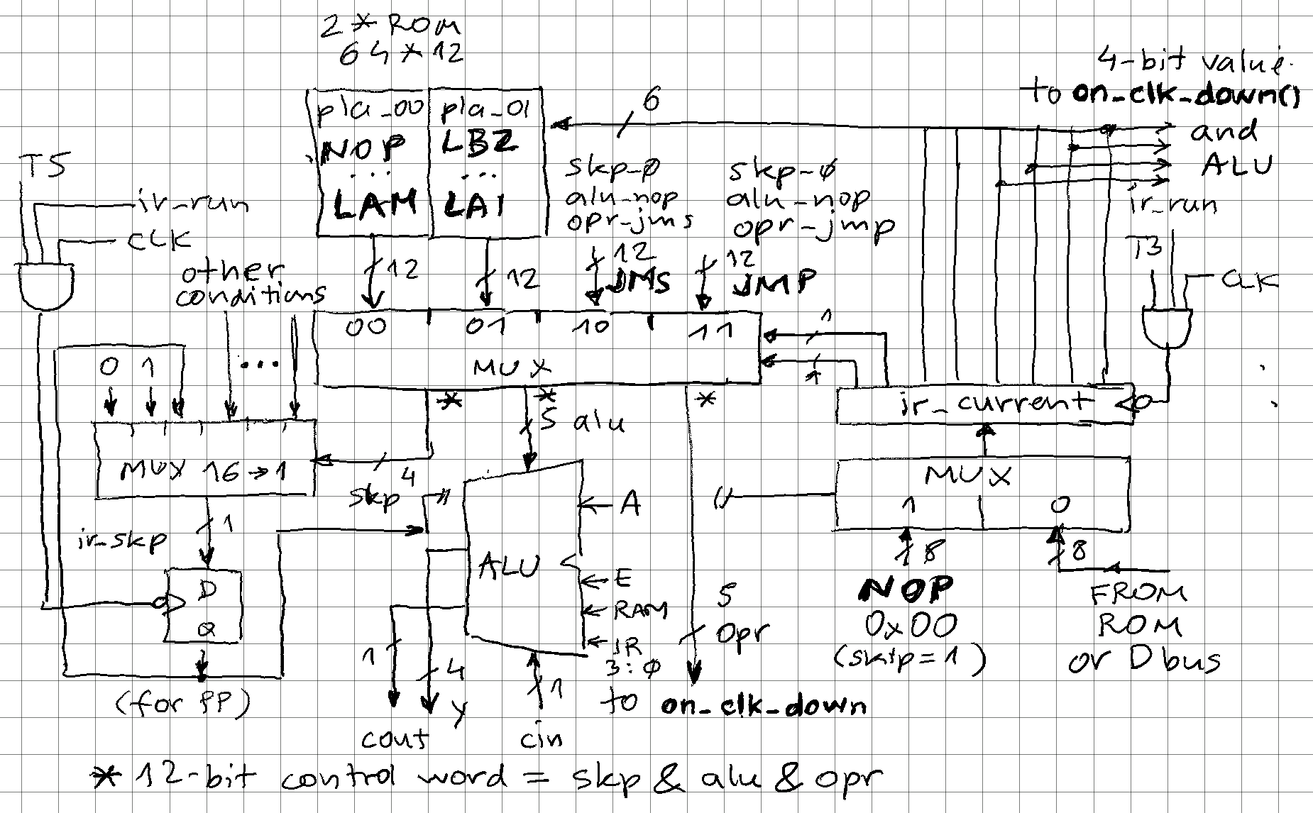
    Obviously, a lookup-table is needed to map from instruction op-code to the corresponding control signals. This would be a 256*12 ROM, but because JMS and JMP would be repeat 64-times, splitting the instruction space to 4*64 with a 4 to 1 MUX tied to instruction registed bits 7 and 6 allows cutting this memory requirement in half:

    -- instruction decode (256 op-codes split into 4*64 blocks)
    with ir_current(7 downto 6) select pla <=    
        pla_00(to_integer(unsigned(ir_current(5 downto 0)))) when "00", -- NOP to LAM    
        pla_01(to_integer(unsigned(ir_current(5 downto 0)))) when "01", -- LBZ to LAI    
        skp_0 & alu_nop & opr_jms when "10",      -- JMS    
        skp_0 & alu_nop & opr_jmp when others;    -- JMP

    We see how JMS and JMP are defined as a concatenation of 3 control fields, pla_00 and pla_01 hold these for all the other instructions. "pla" (programmable logic array) is a mis-nomer here because these are simple ROMs, no AND/NOT/OR logic array, but could be implemented in that way.

    The MUX above is central piece of the instruction decode logic:

    Resulting 12-bit control word is drives most of the processor internals:

    -- instruction decode
    signal pla: std_logic_vector(11 downto 0);
    alias skp: std_logic_vector(3 downto 0) is pla(11 downto 8);
    alias alu: std_logic_vector(2 downto 0) is pla(7 downto 5);
    alias opr: std_logic_vector(4 downto 0) is pla(4 downto 0);

    skp - skip

    skp is driving a MUX that selects the 1-bit flag or value to load into ir_skp register, which will be checked to either execute the instruction or mask it with 0x00 to become a NOP (which has same effect as skipping). Note the value for PP (prepare page) - skip bit is a pass-through so that is 1 PP is skipped, any subsequent is skipped too. This allows conditional JMP/JMS to any location, not just on current page. 

    -- select source for updated skip flag (16 to 1 mux)
    with skp select y_skp <=
    --		'0' 	when skp_0,	-- never skip next instruction
    		'1' 	when skp_1,	-- always skip next instruction
    		ir_sec  when skp_sec,
    		bl_equals_e when skp_ble,
    		(not mr_cy) when skp_cy0,
    		(not y_alu(5)) when skp_cout,
    		a_equals_m when skp_am,
    		(not bit_is_1) when skp_bit,	
    		bl_is_15 when skp_blf,
    		bl_is_0 when skp_bl0, 
    		not(ik(3) or ik(2) or ik(1) or ik(0)) when skp_ik,	-- at least 1 zero detected in I or K after masking	
    		ir_skp when skp_skp,	-- do not change skip flag, pass it to next instruction
    		mr_f1 when skp_f1,
    		mr_f2 when skp_f2,
    		'0' when others;	-- no skip by default

     alu -...

    Read more »

  • Running it on BaSys2 FPGA board

    zpekic12/26/2022 at 11:54 0 comments

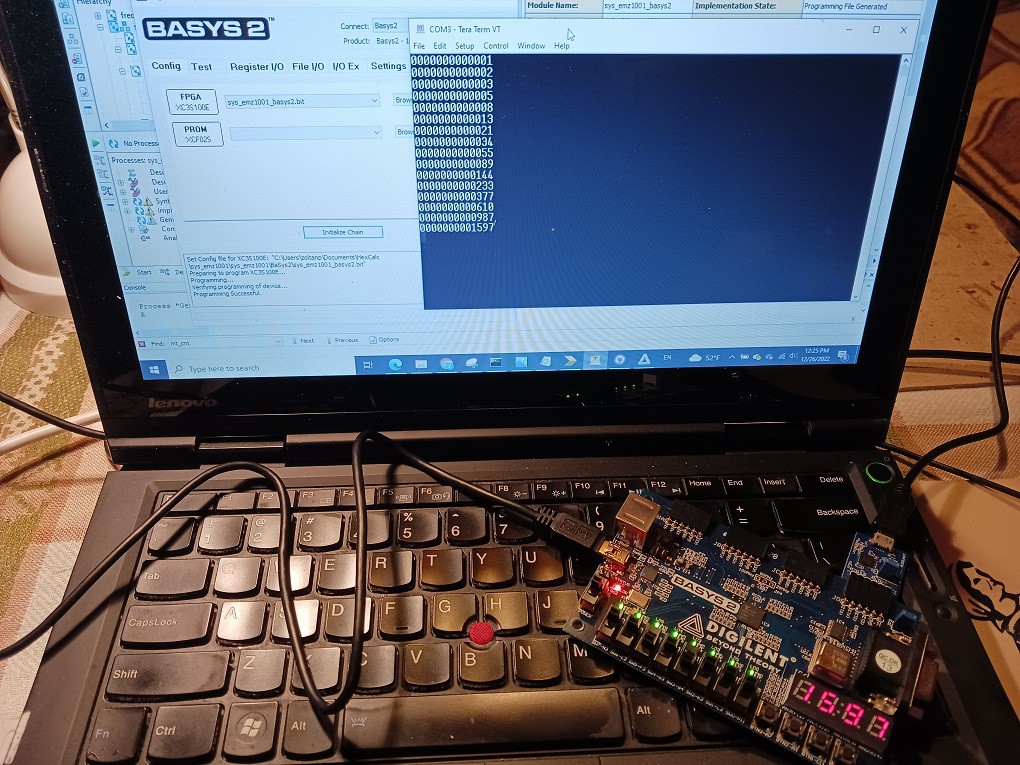
    As I was travelling, I left my Mercury board behind, but I had a older Digilent BaSys2 FPGA board at hand so I modified the design to fit:

    • FPGA chip is more modest so I disabled the whole VGA subsystem (VGA controller + video RAM + TTY circuit would not fit)
    • There is no separate RESET button, it is not of much need but press on 4 buttons at the same time causes reset
    • 7seg display segments were ordered differently so they needed to be reshuffled to show correct digits / letters
    • There are 8 LEDs on the board, I used them to display dbg_mem and dbg_ram - not much use, but some "blinkenlights" are always good :-)

    The top level project source code file is here, and the pic of working board (with first Fibonacci numbers sent to UART) below:

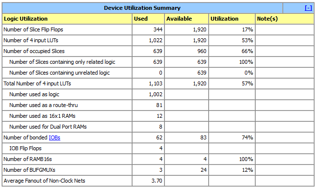
    Because this pretty much bare-bones EMZ1001A + 1k internal + 1k external ROM, it illustrates the amount of FPGA resources usage. Such modest usage would allow embedded EMZ1001A to be used as simple controller in other FPGA-based designs when 8-bit cores can be an overkill:

  • Test code - Fibonacci sequence generator

    zpekic12/12/2022 at 05:46 0 comments

    Why Fibonacci sequence? The algorithm is simple enough to fit into code and data memory, and allows to test lots of the processor functionality:

    • LED display and refresh, with DISN (display numeric) mode
    • OUT 8-bit values (generating ASCII text stream for VGA and UART)
    • Simple arithmetic (BCD additions)
    • 1 second timer
    • Subroutine calls over different pages, including "default" page 15

    Description below refers to the code here, note that line numbers and labels may differ as I still tweak the program a bit.

    The most common application of EMZ1001A were in small appliances or devices with simple capacitive keyboard and few LED 7-segment digits (for example, a microwave oven, digital scale etc.). For these to be useful, LED display must at all times display some correct data continuously. Interrupts do not exist, instead the display refresh is the main loop of the program, and everything else that needs to happen must be done within that dead loop (old calculators worked the same way, that's why during calculation their display was momentarily blank or scrambled). 

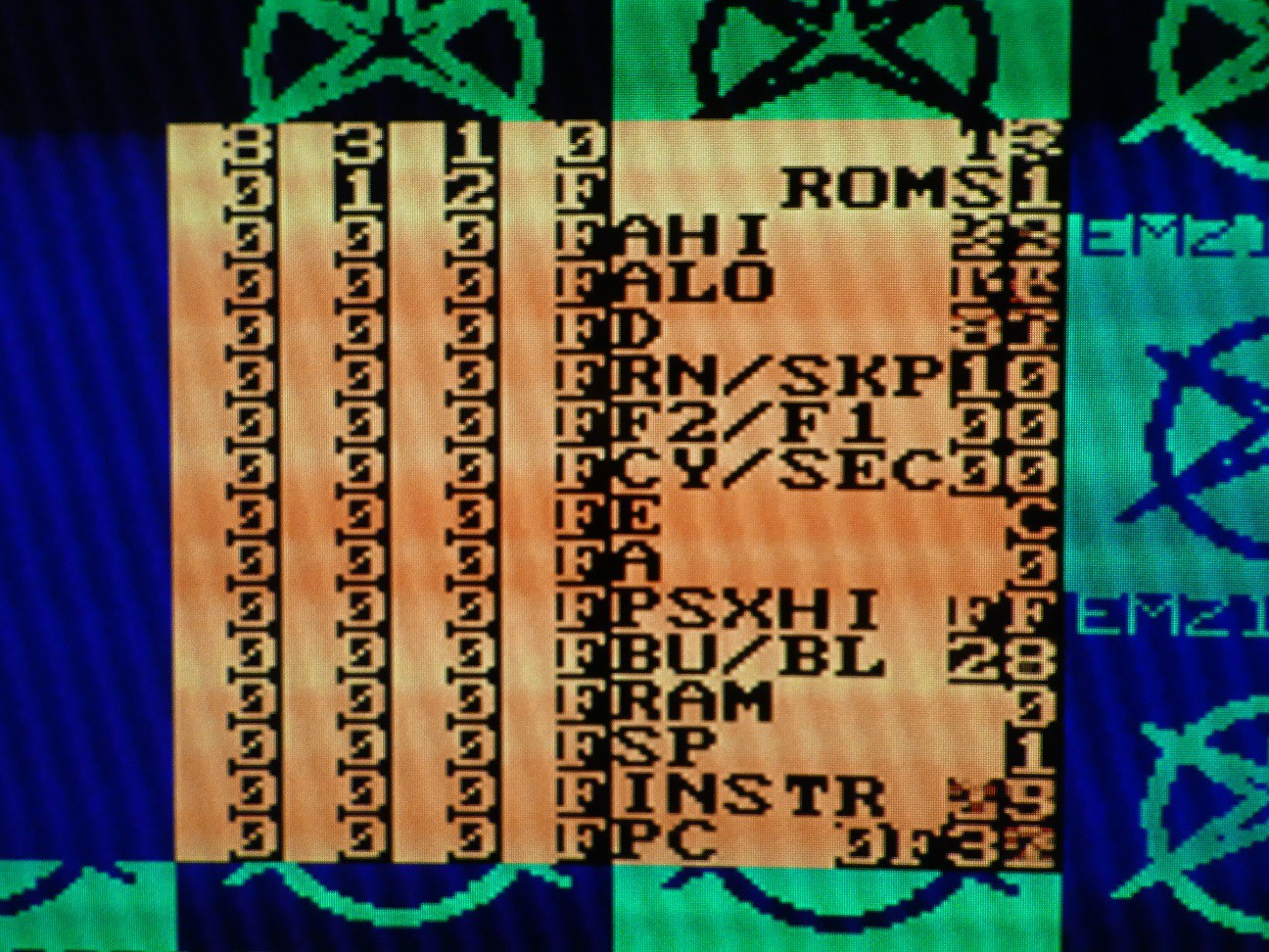
    LED display can be only driven from RAM location, so at the time of LED display update RAM must contain valid data, in this case a valid Fibonacci number in the sequence. It is held in bank 2 (used for display), and previous 2 numbers are in banks 0 and 1. The debug display on VGA illustrates the placement of data (8+13 = 21):

    So the algorithm is:

    1. Initialize the processor
    2. clear bank 0 (column 0 in the pic, now contains 0000000000000000)
    3. clear bank 1
    4. flip LSBit of LSDigit in bank 1 to 1 (so it now contains 0000000000000001)
    5. Add banks 0 and 1 and store to bank 2 (BCD add)
    6. Display bank 2
    7. Go back to step 6 and refresh LEDs until 1s tick is detected
    8. copy bank 1 to 0 and 2 to 1 (so we have always the previous 2 numbers in banks 0 and 1)
    9. go to step 5
    10. BUG: I wanted to detect carry from MSDigit to restart from 0 but somehow it is missed so it continues indefinitely generating last 13 valid Fibonacci decimal digits)

    While the processor is relatively simple, it does have some clever capabilities that can be used to accomplish some tasks efficiently. Few highlighted below.

    Looping over RAM locations

    64 nibbles can be thought as a 2D 4*16 array, addressed by BU (2 bit) and BL (4 bit) registers. Loops can be started at any BU and BL either 0 or 15 and then traversed towards the opposite end. End condition is baked in into the instruction based on the direction of the BU increment/decrement direction. Example:

    DEADLOOP:   LBZ 0;        // select RAM column 0, row 0
                JMS  CLEAR;    // clear RAM column 0
                
                LBZ 1;        // select RAM column 1, row 0
                JMS  CLEAR;     // clear RAM column 1
    
    (omitted)
    //    ---------------------------------------------------------------------------
                .org 0b1111000000;
    //    Page 15 in the bank is the default place for subroutines
    //    ---------------------------------------------------------------------------
    CLEAR:  LAI 0;            // A = 0, BU set by caller
            XCI 0;            // Exchange with M[BU, BL], BU = BU, BL++
            JMP CLEAR;        // repeat until all covered (BU = 0)
            RT;                // back

    Efficient and fast subroutine calls

    Program memory can be up to 8k (13-bit address), but JMS instruction has only 6 - where does the rest come from? Best if from nowhere (it is implied) - unless PP was executed before (to change the page), JMS will jump to [curent bank][page 15][6-bit destination]. Storing entry points of subroutines on page 15, and only if that page does not have enough space (1 page = 64 locations), branching with PP + JMP to the final destination. Example:

    (on page 0)
    
    ADDLOOP: JMS  BCDADD;    // RAM[2,*] = RAM[0,*] + RAM[1,*]
    
    (on page 15)
    
    BCDADD: LBZ 0;           // BL = 0, BU = 0
            RSC;             // clear carry
    ALOOP:  LAM 0b01;        // A = M[0, BL], BU = 1
            ADCS;            // C,A = A + M[1, BU] + C
         JMS...
    Read more »

  • Test code - "HELLo WorLd!"

    zpekic12/12/2022 at 05:43 0 comments

    (Refer to "Hello World!" example in EMZ1001A assembler for code discussion below)

    "Hello World" is expected to show case any new programming language, and EMZ assembly has been resurrected along with the "chip" so it seemed perfect to use it as a default "firmware" that goes inside the 1k ROM.

    It simply rotates (in 1 sec intervals) the text on 7seg LED display (DISB instruction), and outputs the ASCII character sequence (plus CR and LF) using OUT instruction. Algorithm is:

    1. Initialize operating modes (most important is to not float D lines to be able to drive TTY and UART inputs)
    2. Initialize RAM with the 7seg LED patterns of "HELLo WorLd!" string - this is 12 characters, so remaining 4 are set to zero (no segment lit up)
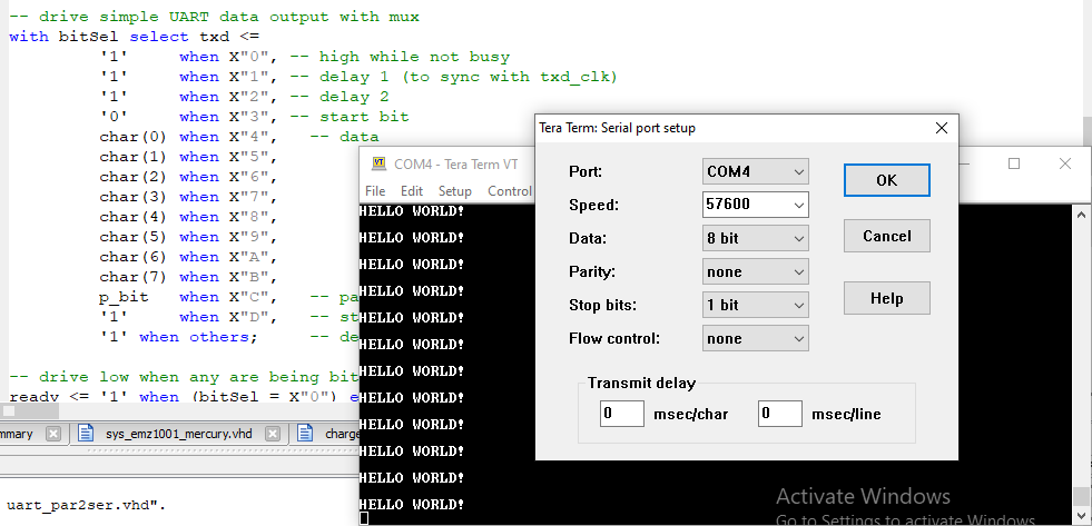
    3. Output "HELLO WORLD!" to UART and TTY (each character is a JMS call to a character-specific entry point)
    4. Refresh the LEDs (run DISB in loop for all BU values)
    5. Check if 1 second has expired, if no go to step 4 (this keeps LEDs lit!), otherwise continue
    6. "rotate" values in RAM banks 0 and 1 - this achieves the "scroll every 1s" effect
    7. go back to step 3 for infinite loop

    Weird but clever LAI

    As per documentation, only first LAI (Load Accumulator Immediate) instruction in a sequence is executed. There is an internal flag which is set by LAI and reset by any other instruction, and if true, LAI becomes a NOP. This strange but simple trick allows easy implementation of multiple entry points into a subroutine, while saving many instructions jumping over the alternate paths:

    GREETINGS:    LBZ 0b11;        // BU = 3, BL = 0 
            JMS CRLF;        // empty line
            JMS H;            // output character by characted on D port, with nEXT strobe
            JMS E;
            JMS L;
            JMS L;
            JMS O;
            JMS SPACE;
            JMS W;
            JMS O;
            JMS R;
            JMS L;
            JMS D;
            JMS EXCPOINT;
            JMS CRLF;
    ...
    
    H:        LAI 0x0F & 'H';    // using EMZ1001A trick that in a sequence of LAIs only 1st one is executed!
    E:        LAI 0x0F & 'E';
    L:        LAI 0x0F & 'L';
    O:        LAI 0x0F & 'O';
    D:        LAI 0x0F & 'D';
    OUT_4:        RSM 3;        // high nibble is 0b0100 for these ASCII codes
            STM 2;
            JMP OUT_xx00;
    

     4 JMP instructions are saved in the sequence above. In additional trick, characters are grouped by value of upper nibble of ASCII code, and convenient RSM (reset memory bit) and STM (set memory bit) can directly update RAM without disturbing the A register. 

    OUT instruction - simple but effective

    Both DISB and OUT output 8-bit data on the D bus - when not in float mode and not multiplexed for use as ROM data inputs. The difference is strobing:

    • OUT - nEXT goes low during T7
    • DISB - nEXT stays high, but A strobes the LED digit (high or low)

    Both TTY (to VGA) and UART (parallel to serial) take 8-bit ASCII data, so their input is connected to D, and strobe (inverted) to nEXT. That means 1 OUT sends ASCII character simultaneously to both with the effect of "print" (even a simple unidirectional Centronics interface could be added for a real print), but only if they are both ready as sensed by input line I0 (there is no FIFO buffer between CPU and output devices, so the output speed is effectively limited by baudrate / 16). 

    CRLF:       LAI CR;
                JMS OUT_0;    // old assembly trick
                LAI LF;
    OUT_0:      RSM 3;        // set current RAM location to 0
                RSM 2;
    OUT_xx00:   RSM 1;
    OUT_xxx0:   RSM 0;
    UART_OUT:   OUT;
    UART_WAIT:  LAI OUT_READY;  // connected to pins 0, 1 of I inputs
                SZI;            // skip if low
                RT;             // signal high, ready
                JMP UART_WAIT;  // signal low, not ready

    Note: more optimal implementation would first check for readiness and then if ready proceed to OUT and return - this way fewer instructions after RT would be blocked, and a simple "parallelization" of CPU operation and 2 output devices operations could be achieved. 

    DISB - any pattern to LEDs

    Somewhat readable text can be represented on 7-segment LED with a certain...

    Read more »

  • Recreating a simple EMZ1001A assembler

    zpekic12/12/2022 at 05:40 0 comments

    Any processor - no matter how simple or complex - is of little use if it cannot execute some program. I could not find any listing or ROM code for any EMZ1001A application, the closest was this note about using EMZ1001A as a DMTF frequency signal decoder. In addition, executing a program is the only way to test the instructions, so I decided to write 2 "apps" to validate the processor and demo it.

    Next problem was lack of development toolchain. AMI documentation describes a sophisticated development system that includes hardware and software - with a macro-assembler. Even if this could be found today, it would be not practical to integrate with PC-based FPGA toolchain, so only option was to write own. 

    One approach would be to leverage already existing tools, for example a universal cross-assembler.  Then I realized, I already have written one myself - my micro-code compiler

    How does a 2-pass microcode compiler become a 2-pass assembler? Not easily, except for lucky coincidence that EMZ1001A uses only 8-bit op-codes, which is exactly the same as horizontal microcode, where each microinstruction has exactly the same width (usually 20 bits +), and the number of microinstruction formats is very limited (often times, only 1 format, meaning each field in microinstruction has same meaning in each microinstruction).

    Microcode compiler allows defining multiple fields in the microinstruction (from emz.mcc include file):

    // define any slices of the instruction word format
    f76			.valfield 2 values * default 0;
    f54			.valfield 2 values * default 0;
    f32			.valfield 2 values * default 0;
    f10			.valfield 2 values * default 0;

    With these 2-bit fields, EMZ1001A instructions formats can be expressed as: 

    FormatLayout

    o - opcode bit

    U - operand bit that must appear inverted in code

    X - operant bit that must appear not-inverted in code

    Sample instructions.mcc definition
    8+0ooooooooNOP...DISNopr8 .valfield f76 .. f10 values * default 0;
    6+2ooooooUUSZM, STM, RSM, LB*opr6 .valfield f76 .. f32 values * default 0;
    val2 .valfield f10 .. f10 values * default 0;
    6+2 invertedooooooUUXC*, LAMopr6 .valfield f76 .. f32 values * default 0;
    val2 .valfield f10 .. f10 values * default 0;
    4+4ooooXXXXLAI, ADISopr4 .valfield f76 .. f54 values * default 0;
    val4 .valfield f32 .. f10 values * default 0;
    4+4 invertedooooUUUUPPopr4 .valfield f76 .. f54 values * default 0;
    val4 .valfield f32 .. f10 values * default 0;
    2+6ooXXXXXXJMP, JMSopr2 .valfield f76 .. f76 values * default 0;
    val6 .valfield f54 .. f10 values * default 0;

    To differentiate between inverting and non-inverting formats, simply the "macro" includes the ! symbol which will appear before the operand and result in inverted bits in the binary:

    // 2-bit operand, inverted (0x30 .. 0x3F)
    XCI		.alias opr6 = 0b001100, val2 = 3 & !;
    XCD		.alias opr6 = 0b001101, val2 = 3 & !;
    XC		.alias opr6 = 0b001110, val2 = 3 & !;
    LAM		.alias opr6 = 0b001111, val2 = 3 & !;
    
    // 2-bit operand, not inverted (0x40 .. 0x4F)
    LBZ		.alias opr6 = 0b010000, val2 =;
    LBF		.alias opr6 = 0b010001, val2 =;
    LBE		.alias opr6 = 0b010010, val2 =;
    LBEP		.alias opr6 = 0b010011, val2 =;

    With this, it is possible to easily define each EMZ1001A instruction and write assembly code similar to the original (main difference is that each line must end in ; and that the comment character is different //)

    In summary, I had to make 3 changes to existing microcode-compiler:

    • Support the include directive so I can include the definition of fields and instructions in each assembly program (implementation line 467+: #include simply recursively calls the Pass0() in which it has been encountered)
    • Fix various bugs in the field definitions when "virtual" fields contain one or more "real fields" (in this example fields f76..f10 are real, but opr8 which spans all of them is virtual. Values can be assigned only to one within the instruction)
    • Allow to use file extension names beside .mcc (so the "apps" have extension .emz for convenience)...
    Read more »

  • Implementation in VHDL - structure and timing

    zpekic12/12/2022 at 05:39 0 comments

    EMZ1001A microcontroller implementation is contained in 2 VHDL source files:

    • emz1001_package.vhd - contains definitions of types (e.g. memory "formats") and functions used in more than one place in the design. The main helper here is a rudimentary Intel .hex file reader that allows memory initialization during build time (so that the memory image with proper content is included in the .bit stream uploaded to FPGA)
    • EMZ1001A.vhd - contains all of the processor logic 

    As of 2022-12-20, everything described in Iskra / AMI documentation is implemented, except:

    • BRK instruction (op code 0x01) - I could not find info what did it do in real device, so right now it is doing a NOP
    • KREF signal - this is of little use on this purely digital system with no analog components. However, it could be implemented by emulating KREF and Kx signals as PWM and then comparing duty cycle ratio between them and if Kx >= KREF, Kx would read as 1
    • Test mode - when ROMS is fed back with negated SYNC, CPU enters test mode which outputs on D lines content of internal ROM. Of great use on "black box" real device, it is of little use here when all the guts of the microcontroller are wide open, including the firmware ROM content placed there

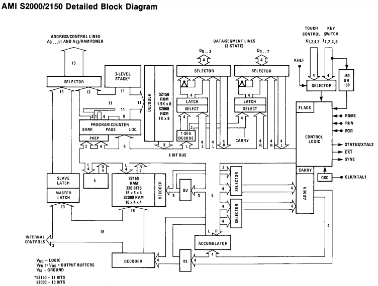
    The "detailed block diagram" from the documentation is not extremely helpful with recreating the device, but still gives some useful hints. 

    • A lines are complex - they are either data outputs from a cascade of 2 13-bit latches, or output 13-bit instruction address if accessing external memory
    • D lines are even more complex - there are 2 output modes (OUT / DISPx) and 2 input modes (INP and reading instruction from external memory), all dependent of CPU mode of operation, SYNC state and instruction
    • Stack depth is 3 (or 4), but width is only 10 bits - 3 bits to select 1k bank are not on the stack. This means that it is possible to JMP from bank to bank, but not JMS (you can go, but can't return :-))
    • PP staging registers (page, bank, and which one is next to be updated) are indicated with "PREP" on the diagram
    • Some internal paths are 8-bit which is interesting for a 4-bit CPU as it allows higher internal bandwidth for simultaneous execution of multiple operations

    Timing

    EMZ1001A has a very rigid timing: all instructions are executed in 1 machine cycle, machine cycle has always 4 clock cycles (T1, T3, T5, T7) and 2 phases (SYNC low - instruction fetch, and SYNC high - instruction decode). Implementation presented here is cycle accurate and follows the real device based on what I could infer from documentation.  2 outside clock sources are consumed, which drive 3 "processes" (VHDL term for defining how registers are updated):

    ClockCLK (CPU operating frequency)I3 (assumed to be A/C mains 50Hz or 60Hz)
    low to high transitioncapture state of RUN, K, I inputs during cycles T3, T5, T7 respectively 

    on_clk_up: process(CLK, nPOR)
    count up until limit set by EUR is reached at which point set a flag that can be consumed by SOS to skip

    on_i_clk: process(nPOR, i_clk, sos_clr)
    high to low transitionAdvance through T1, T3, T5, T7 cycles (using a 1-hot ring counter) and tie almost all of internal register updates based on cycle, run mode, current instruction

    on_clk_down: process(CLK, nPOR)
    N/A
    async (reset condition)Initialize internal registers (except 64 nibble RAM)clear counter on reset, clear flag on reset and SOS execution

    Main action is in the on_clk_down: process(CLK, nPOR). RUN and SKIP indicate the states of ir_run and ir_skp flags.

    AlwaysRUNRUNNO RUNNO RUN
    At the end of:SKIPNO SKIPSKIPNO SKIP
    T1Capture ROMS state in the middle of SYNC low----
    T3-Load instruction register with NOP (0x00)Load instruction register from ROM(PC)--
    T5Capture ROMS state in the middle of SYNC highUpdate skip flag
    Increment PC
    Execute NOP
    Update skip flag
    Increment PC
    Execute all instructions except JMP, RT, RTS
    JMS: increment stack pointer
    --
    T7--JMP and JMS: update PC based on 6-bits in the instruction and state of PP prepared registers...
    Read more »

  • System description

    zpekic12/12/2022 at 05:38 0 comments

    In order to thoroughly test the EMZ1001A implementation, and to make a fun, demo-able system that is "doing something", a small "computer" has been created on the FPGA board, with various components supporting the microcontroller operation. 

    Basic features are:

    • Execution of 2 pre-loaded programs ("Hello World" from internal memory and "Fibonacci" from external) - selectable by switch
    • Output on 4-digit 7-segment LED (multiplexed using A[ddress] and D[ata] lines)
    • Output of 8-bit ASCII (D[ata] lines, strobed with /EXT), these characters are simultaneously output to: 
      • 640*480 VGA which contains a 32*32 text screen (for "teletype" output) and 16*16 window to display debug info
      • UART, which connected to PMOD USB allows host computer to receive output
    • RUN/STOP, single step mode
    • CPU clock selection from single step to 6.25MHz in 8 steps
    • Baudrate selection from 600 to 57600 bps in 8 steps
    • Debug info on VGA screen visualized 64 nibbles of RAM and other most important CPU registers

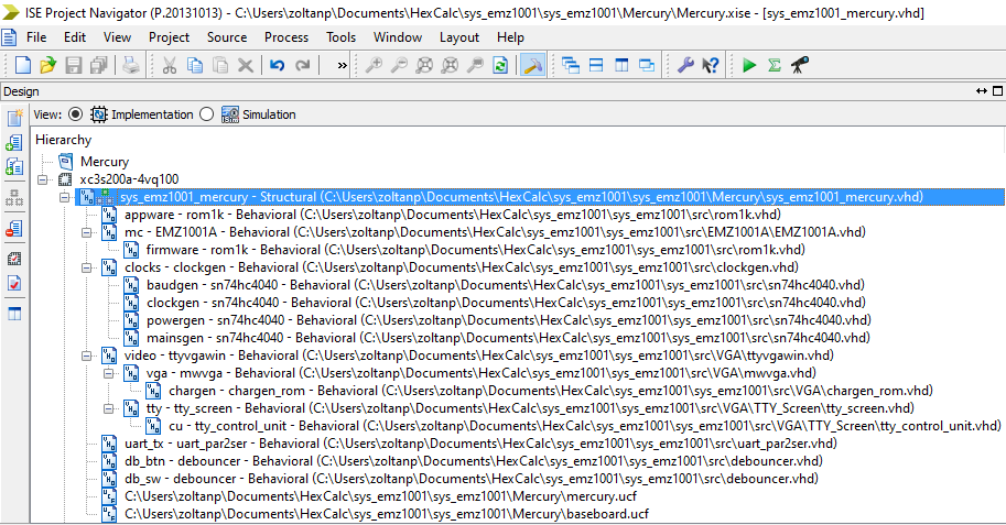
    The system components are coded in sys_emz1001.vhd which is also the top level source file of the design:

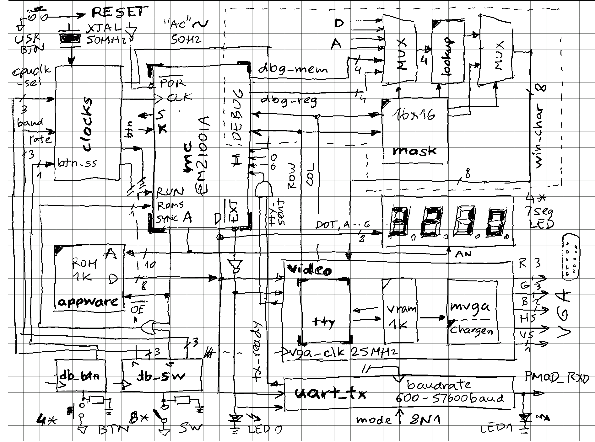
    Somewhat simplified schema of main components (bolded names can be found in the code):

    RESET 

    Mercury board has a USR_BTN which can be conveniently used as master reset. This is a positive logic signal, and is used as such by most components, except by the mc which has a negative active /POR (power on reset) signal.

    clocks

    Unlike many microcomputer designs which can get away with few clocks (e.g. classic Z80 with 4MHz XTAL and a 74LS04s to create a workable oscillator) this one uses many, all derived from internal Mercury FPGA 50MHz clock signal and generated by the clockgen.vhd component. Main are:

    • 25MHz vga_clk - used as VGA dot clock
    • cpu_clk which can go from single step (4 presses on BTN0 goes through T1, T3, T5, T7 phases of machine cycle)
    • baudrate (600 - 57600 bps) - for UART
    • 50Hz - simulate frequency of mains AC to be consumed by SOS instruction to time 1s intervals
    • debounce_clk - drives the debouncers for switches and buttons


    db_btn, db_sw

    12 debouncers are programmatically generated during build time and hooked up to 8 switches and 4 buttons on Mercury baseboard. The debouncer.vhd is a glorified 8-bit shift register clocked by debounce_clk which "votes" the output based if all stages are in same state, and if not, keeps existing state. It is a very simple digital signal filter.

    -- Switches on baseboard
    -- SW(0) -- BAUDRATE SEL 0
    -- SW(1) -- BAUDRATE SEL 1
    -- SW(2) -- BAUDRATE SEL 2
    -- SW(3) -- OFF: EXTERNAL ROM, ON: INTERNAL ROM
    -- SW(4) -- CPUCLK SEL 0
    -- SW(5) -- CPUCLK SEL 1
    -- SW(6) -- CPUCLK SEL 2
    -- SW(7) -- OFF: STOP, ON: RUN
    
    SW: in std_logic_vector(7 downto 0); 
    
    -- Push buttons on baseboard
    -- BTN0 - single step (effective if SW(6 downto 4)) = "000"
    -- BTN1 - not used
    -- BTN2 - not used
    -- BTN3 - not used
    
    BTN: in std_logic_vector(3 downto 0); 

     For example: 

    All switches off: 600 baud, external ROM (Fibonacci), CPU single step (using BTN0), stopped

    All switches on: 57600 baud, internal ROM (Hello World), 6.25MHz CPU, running

    appware

    Simple 1k*8 ROM is mapped as lowest 1k out of 8 possible banks as "external ROM" and is holding the Fibonacci code. Same rom1k.vhd component is also used to define the "internal ROM" which lives inside the EMZ1001A, also in the first 1k memory bank.

    Contents of ROM is initialized during build time, by loading the Intel .HEX file produced by microcode compiler (see "recreating a simple assembler"). This is done by invoking a function which returns a byte array of 1024 elements, defined in the emz1001_package.vhd file. 

    uart_tx

    This is the "parallel to serial" half of a full UART - I use it often in projects to transmit to host PC, using USB to PMOD connector. It is hard-coded to 8 bits, 1 stop, no parity, but the baudrate can be selected using switches 2, 1, 0. Implementation-wise, it is a glorified 16 to 1 MUX. It also...

    Read more »

View all 9 project logs

Enjoy this project?

Share

Discussions

Ken Yap wrote 12/17/2022 at 06:51 point

Hi there, you certainly do come across strange fascinating beasts. Looking forward to reading the progress of this. 👍

  Are you sure? yes | no

zpekic wrote 12/17/2022 at 07:03 point

Thanks a lot for the interest! Yes, I am filling out the logs as I find time, there are interesting things to learn from this old microcontroller, it is simple yet it has some clever tricks that I had to learn to create the test programs. 

  Are you sure? yes | no

Similar Projects

Does this project spark your interest?

Become a member to follow this project and never miss any updates