Arya
Arya-
7) Combining everything into a .fzp
12/14/2016 at 01:23 • 0 commentsIf you want to create your very new part, here's the short way to do it:
- Copy a part from the stock library to "My parts" library
- Place the part you want to copy on breadboard/PCB/schematic
- While it's selected, go Part->Edit
- Go to File and use Save as new part
- Locate the part in your Documents folder
- It'll be in Documents/Fritzing/parts/user
- Throw in your svgs in parts/svgs/user
- In Parts editor, use the File->Load image for view to load new SVGs for the currently selected view (Breadboard/Schematic/PCB/Icon)
- You can also map pins to SVG elements there, though I didn't try it out myself.
- You can also edit pin descriptions, metadata and any XML fields
- Basically, Part Editor is a powerful thing.
![]()
So, the .fzp is just an XML file and if all fails, you can edit it easily. Adding pins to an XML is maybe the only troublesome task - if you need more pins, you could probably write a macro for copy-pasting those since manually copying and pasting those <connector> blocks is very simple but time-consuming and easy to make a mistake in. Link any SVGs you want, experiment away and it should work. If it doesn't, Ctrl+Z until it does and repeat the changes one-by-one.
Fritzing also has a Part->Regenerate part database menu entry, I figure it could help if you changed something by editing XMLs and something doesn't link with something. Anyway, if something doesn't link - regenerate database, restart Fritzing and so on.
- Copy a part from the stock library to "My parts" library
-
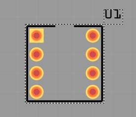
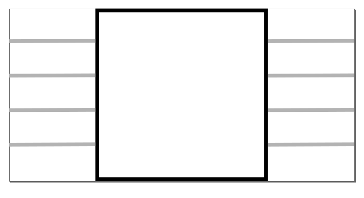
6) Simple guide - making the PCB footprint
12/14/2016 at 00:12 • 1 commentA very simple footprint. Fritzing generates those automatically, again, and this is how it looks:
![]()
Couldn't have done it simpler.
New Inkscape document:
Canvas dimensions:
- Width: whatever is width of your package in 0.1inch units, plus 0.02in for outline
- Height: number of pads from one side * 0.1inch, plus 0.02in for the outline again
That leaves us with 0.42x0.42in.
By @Radomir Dopieralski's suggestion, let's turn the grid on (View->Page Grid). You can snap to it, which should theoretically decrease the amount of "Transform->Move" we have to do to align everything.
Silkscreen layer:
Draw lines at the contour, for the outline. With the grid, I just drew a path (Straight line tool, draw lines by left click, end drawing by right click). Will see how it works, but it looks great already. Now select the path, group it and ID as "silkscreen". You might also want to color those lines white - while they are selected, point at white in the palette at the bottom and shift-click.
I'd show lines here, but they're white.
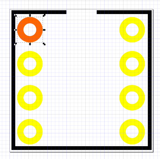
Pads:
Pick a color, you'll be drawing pads and this will ensure they're colored as you place them. Just shift-click on any yellow in the palette you'd like to use.
What you'll be drawing is the copper pads exactly the way they'll appear on PCB. I'll just copy the alignment from the sample footprint, shouldn't be
We'll draw first pad in the left bottom corner.
- Set stroke width to 0.02in
- Set width and height to 0.075in
- Set X/Y position to (0.022, 0.022)in
- Make sure it's the right shade of yellow.
Duplicate part and place 3 more pads at X:0.022in, Y:(0.122, 0.222, 0.322)in. Then four parts at X:0322 and same Y coordinates. It's cooler if you overlay a rectangle on top of the first pin's circle to make it a rectangular pad, I won't (I'll make the pad orange and see how it looks in Fritzing).
![]()
I also colored the silkscreen lines black for you to see. Looks nice!
Grouping and IDs
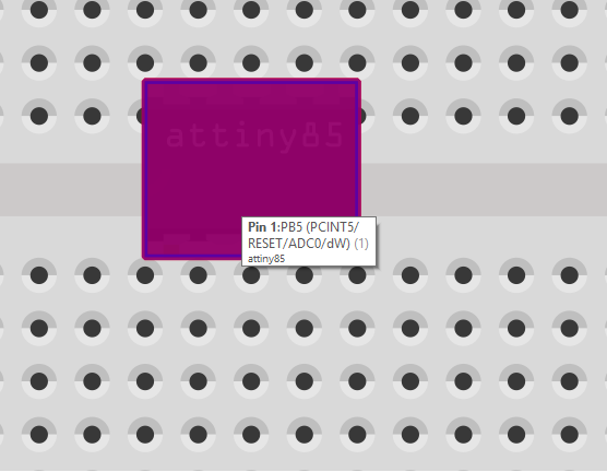
ID the pads as "connectorXpin", where X is from 0 to 7 for us.
Select the pads, group them and ID the group as "copper0". Then select that group. make a group out it and ID it as "copper1". Yes, you should have two nested groups, top group with a single "copper0" group with it. This is a neat trick to distinguish SMD parts from THT parts and show which pad goes where.
If, say, you had an SMD part, you'd only need to use the "copper0" group for your SMD pads. If you had an SMD part soldered to both sides of board (think edge-mounted connectors) and that part had different pad placement on different sides (think of an edge-mounted footprint for a COM port socket), you'd simply put different pads into different groups - top pads into "copper0" group and bottom pads into "copper1" group.
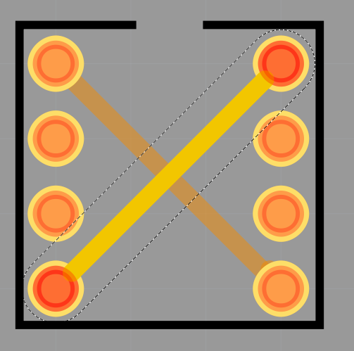
Drew two traces to make sure both bottom and top layers work![]()
That's it! We've got the main 3 views for a component in 3 short guides. The main thing is - you shouldn't even do all that for the most popular parts, thanks to the parts you can repurpose and edit. On the other side, knowing how to create simple things completely from scratch, you can create a footprint for pretty much any part in Fritzing - such as your custom ESP32 breakout board or another weirdly-shaped module you want to use but don't know how to create a part for.
-
5) Simple guide: Making a schematic
12/13/2016 at 18:43 • 0 commentsWe're aiming for a simple schematic symbol - a rectangle, pins from both sides matching the physical pinout and text labels with those.
New Inkscape document:
Canvas dimensions:
- Width: 1 inch
- Height: (number of pins from one side + 1 )*0.1, for our ATtiny it's 5*0.1 = 0.5
IC body:
Draw a rectangle, no fill, black outline with 1px stroke width. Dimension it to 0.5x0.5in and center.
IC pins:
Draw a straight line, set width to 0.25 in and height to something like 0.012. Move first row of lines to X:0.0in and Y:(0.1, 0.2, 0.3, 0.4)in. Second row goes to X:0.75in and same Y.
![]()
IC terminals:
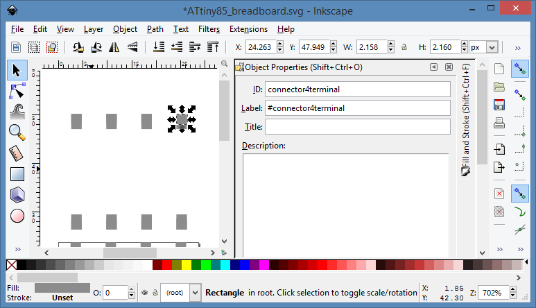
A tricky thing. This is where the lines on the schematic connect to, it's invisible but meaningful. In the original symbol, it was like 0.2x0.2px large (how is 0.2px even a thing) so let's make it as large. As points that small are a pain to select (and it's invisible!), let's copy as much attributes as possible and then duplicate the rectangle and change position&Id for the duplicates.
First terminal:
- Fill and stroke are None
- Scale to 0.2x0.2px
- Apply ID of "connector0terminal"
- Move to 0.0x0.406 (the 6 is there to be centered at the pin we drew, since its width is 0.012)
Other terminal:
- Copy the currently selected pin
- Apply new ID
- Move to 0.0x(0.306, 0.206, 0.106)
For second row, everything's the same, just the X coordinate is 1.0in.
There's no picure of changes because those rectangles are invisible. These were also the hardest to copy, since, well, invisible, and on top of that - under the pin object. I had to keep at least one selected at all times and never lose track of which ones I placed. I can understand why it's so hard though - schematic symbols are supposed to be taken from some IC/autogenerated.
IDs and text
Place txt labels - any labels you'd want to appear on the schematic. Also, ID the pin lines as "connectorXpin", where, X would be from 0 to 7 in our case.
Result![]()
It works! there's something wrong with the text, but you guys are smart enough to figure it out.![]()
-
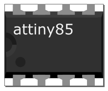
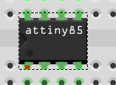
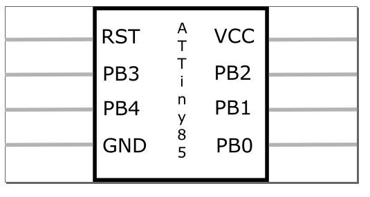
4) The simplest guide - DIP/SIP/SMD in 2 minutes!
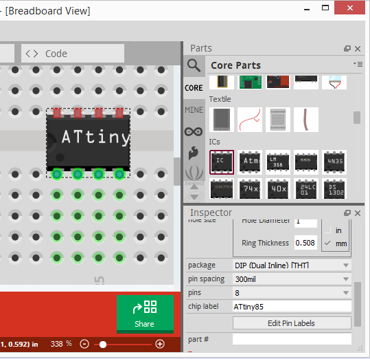
12/13/2016 at 17:03 • 0 comments- Open Fritzing
- Part window is on the right of Fritzing window, go to Core parts
- In "ICs" section, select the first one - with "IC" on it
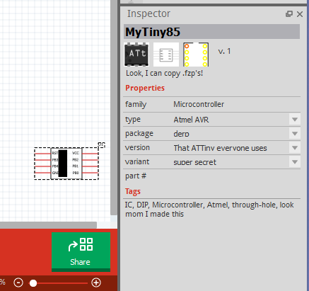
- Inspector window is right under the Parts window (if not, go to Window->Inspector), we need the Properties section
- In that section, you can select your package type (DIP/SIP/various SMD options), variant, number of pins and even label your IC any way you want.
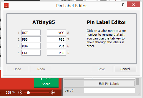
- Edit the pin labels.
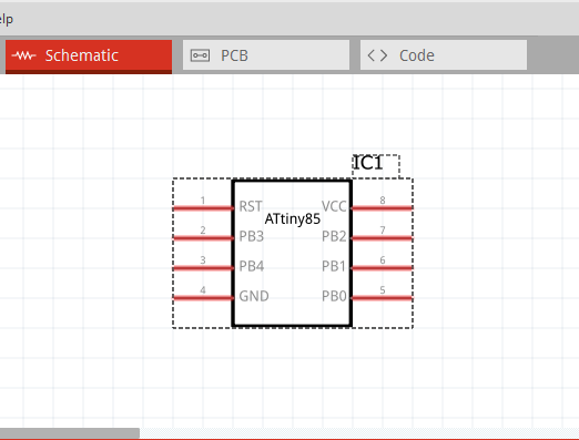
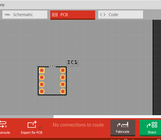
Everything is autogenerated. For even better effect, select the part and go Part->Edit . I didn't even need that to make an ATTiny.
Problems:
- I don't know if a part like this is easily distributable, didn't find any button to export a part (I saw one candidate but it was greyed out).
- I didn't see any setting to make a wider DIP footprint (as in - for bigger ICs) like old CPU/RAM/ROM chips etc. It probably can be done the "part from scratch way", but the setting might also be already there.
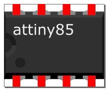
![]()
![]()
![]()
![]()
-
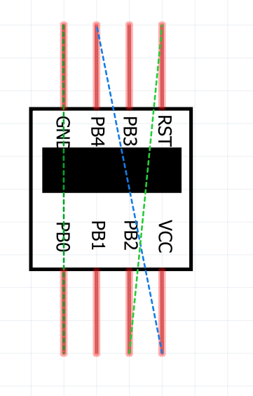
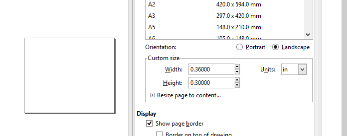
3) Simple guide: breadboard footprint and Inkscape crash course
12/13/2016 at 16:09 • 2 commentsATTiny85
Measurements and preparations:
- IC dimensions (with pins) - 0.36x0.30in
- IC body dimensions - 0.36x0.23in
- Dimensions between pin centers - 0.1in
The SVG we'll need to draw will be a little larger though to look nice and be perfectly aligned with the grid. Let's say pin rectangle height will be 0.035.
Modifications:
- IC dimensions (with pins): add 0.04 to width amd height
- IC body dimensions - multiply pin rectangle height by 2 and subtract that from IC body height, body width stays the same
Resulting dimensions for ATtiny85:
- IC dimensions (with pins) - 0.38x0.34in
- IC body dimensions - 0.38x0.27in
Inkscape usage
Save your SVGs as "Plain SVG" (File->Save as...) This will prevent Inkscape from inserting unnecessary tags, you just have to remember to do it each time you save your changes.
Changing canvas dimensions: New document, Page-> Document Properties, set dimensions and units inches.
How to dimension things: Object->Transform->Scale (might need to uncheck "proportional"), set dimensions to
How to center and align relative to canvas/other things: Object->Align and Distribute, it has various icons, Align section has the ones we need.
How to color things: Object->Fill and Stroke, stroke is object outline.
How to ID things: Object->Object Properties, the ID field.
How to group things: select things you want to group and Object->Group.
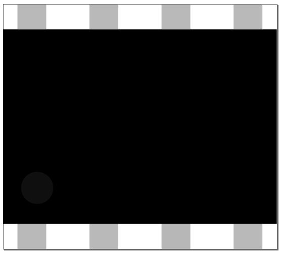
Drawing the IC body
![]()
Draw a rectangle, dimension to 0.38x0.27in. Align to vertical/horizontal canvas center. Fill with solid black. Draw a circle to mark the first IC pin, and make it 1c1c1c grey.
Drawing the IC pins
![]() Draw grey rectangles. Height is 0.035 as we defined in the beginning, width is about the same, better if it's an even number - like 0.04. Y coordinate is simple to determine - just vertical align top pins to top canvas line, and bottom pins to bottom canvas line. X coordinate calculation:
Draw grey rectangles. Height is 0.035 as we defined in the beginning, width is about the same, better if it's an even number - like 0.04. Y coordinate is simple to determine - just vertical align top pins to top canvas line, and bottom pins to bottom canvas line. X coordinate calculation:- They'll be different by 0.1 - that's the pin spacing. The spacing between pins will be 0.3in long, so we have 0.08in left from both sides, thus 0.04in from top left corner to top left pin center
- X coordinates are taken from bottom left corner of pin rectangle, so subtract half of pin length from that topleft pin center coordinate we got. We get 0.04-(0.04/2) = 0.02.
- Thus, pin coordinates start from 0.02. We get 0.02, 0.12, 0.22 and 0.32 - that's for both top and bottom rows.
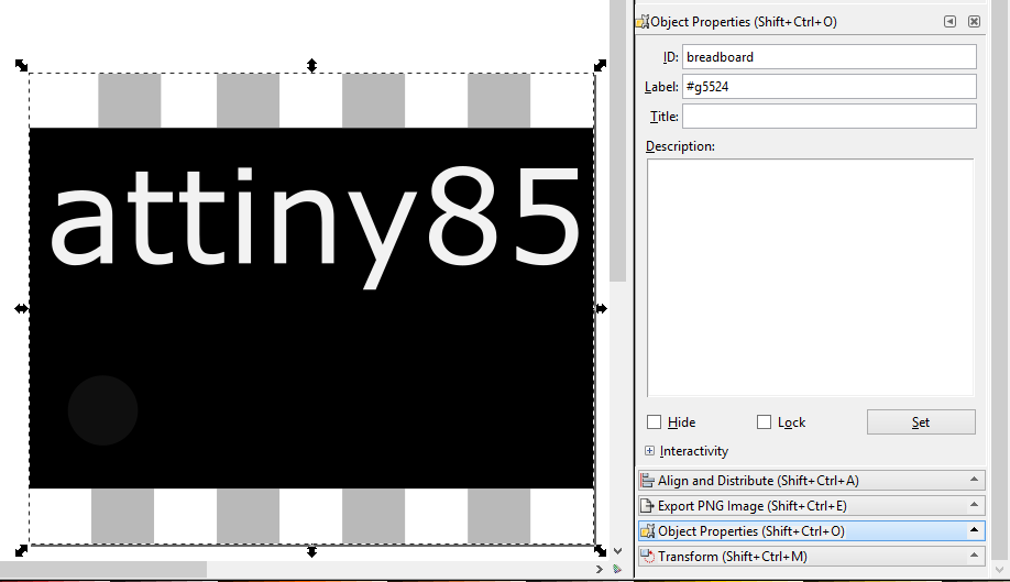
Finishing touches - text and IDs
![]()
Place some text where you want, adjust the font size till it fits right.
Give IDs to your pins - they should look like "connectorXpin", for us X is a number from 0 to 7.
Select all, group it and ID it as "breadboard".
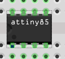
Footprint ready!
-
2) Making a footprint from scratch
12/13/2016 at 02:54 • 2 commentsThe footprint I got minified is a good template. I could just put "ATtiny85" into "ic_text"... come to think of it, it's already there. However, let's make it from scratch! There'll be issues like grid sizes and dimensions and it would be unfair not to get those sorted out.
Woke up, continuing work. Does the size even matter? I measured the real Tiny's dimensions and they weren't to scale with the SVG. Let's scale our ATtiny85 in Inkscape to those dimensions and find out:
![]()
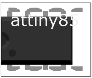
Well. First of all, I enlarged that footprint but it shrinked. Second thing - Inkscape fucks up the SVG, making it unreadable:
![]()
What Inkscape does is effectively un-minifying the XML tree and adding its own tags. Ah well, I guess we could live without the pretty view - the main problem is scaling.
Next attempt - scaling the Tiny, but not the canvas - now preserving the ratio and just scaling up some pixels:
![]()
Ahha, so canvas size matters. Scaling the canvas up:
![]()
Okay, must have fucked something up while scaling. The important question is - what is defining the size as seen in Fritzing? I'll try to get through XMLs to find out...
No avail. Okay. Delete the "breadboard" XML ID and see if it snaps to grid...
It does. Change the pin IDs...
It still does. Wonderful... Not. Removing two pins from both SVG and .fzp:
Fuck it. Restarting Fritzing (oh god it's slow):
![]()
Successfully fucked up. Seems like something was cached. I can even almost figure out the caching process! Now, onto changing the breadboard and pin IDs back - except that I'm removing one pin from SVG and .fzp...
Nop. Still fucked up. Restarting Fritzing and trying again:
![]()
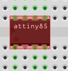
Success. However, the part is now colored red and is hard to move. Restoring the "connectors alright version" and restarting Fritzing...
Not red anymore? Maybe connectors have to be numbered right? Removing the Pin number 8 and retrying...
Pin 8 removed, part is red again. Is the .fzp I'm using even right? Returning the pin 8, changing its description, restarting the Fritzing and trying again...
Yeah, description is the old one. Well, to hell with it. I'll stop reverse-engineering things and finally draw a breadboard part:
![]()
Canvas set to max dimensions of my ATtiny85.
![]()
IC body: drawing a rectangle, Transform->Scale, uncheck "proportional", set dimensions to 0.36x0.23in (as measured by caliper). Align and Distribute-> Align -> center vertically and horizontally. Fill and stroke - fill with solid black and 100% opacity. Drawing a circle where it is on my IC, and I'll make it 1c1c1c grey. It's not pretty, but it sure as hell will work.
![]()
Pins are harder - mainly due to alignment issues. Let's divide the 0.36 length into 0.08 segments and center the pins in centers of those segments - that'd be 0.04, 0.12, 0.20 and 0.28. Now how to enter that in Inkscape? Oh, Transform->Move!
Top row vertical coordinate: 0.265in
Bottom row vertical coordinate: 0.000in
![]()
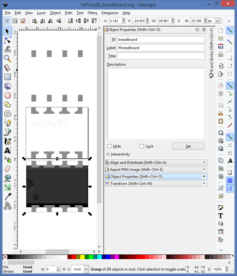
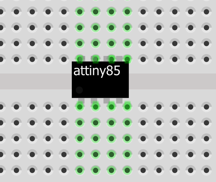
Now, pins get IDs from "connector0pin" to "connector7pin" (Object Properties -> ID). Adding "attiny85" text, select all, create group and name it "breadboard". Should be done! I'll just use the "Plain SVG" export option in Inkscape (in "Save As"), could reduce cruft. Let's replace the original SVG with ours and see how it works:
![]()
Not too good, but works. Some pin repositioning is required, and I might need to enlarge the components a bit. Let's restart Fritzing and check it works though...
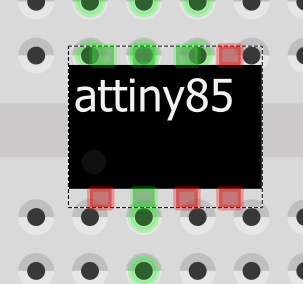
![]()
It doesn't actually, but I'm starting to get a hang of it now. The SVG really does determine pin positioning, it's just cached. Tasklist:
- Try to make that Tiny a little wider and higher
- Place pins on a grid
Solutions:
- Canvas is 0.38x0.32in now, IC body is 0.38x0.25, pins realigned
- Now I think having 0.08 offsets was stupid. Pins are 0.02, 0.12, 0.22 and 0.32 now (X coordinate for the left bottom corner.)
Saving, reloading Fritzing and trying again:
![]()
Success! Except for height, everything is awesome.
Height to 0.34, IC body height to 0.27, restarting, testing...
![]()
Full success. Now, onto boiling it down in a separate worklog!
-
1) See how the existing parts look like
12/12/2016 at 23:50 • 4 commentsNothing's better than reverse-engineering, right?
![]() Well, maybe I can actually learn something from the existing parts, especially provided there are so many DIP-8 ICs shipped with Fritzing. I'm creating everything from scratch, but this saves my frustration for me and time for readers.
Well, maybe I can actually learn something from the existing parts, especially provided there are so many DIP-8 ICs shipped with Fritzing. I'm creating everything from scratch, but this saves my frustration for me and time for readers.Fritzing is huge - 182MB archived, 360MB unpacked. I can go make hot chocolate while the archive is unpacking.
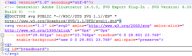
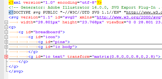
Fritzing has a folder named "fritzing-parts" inside, wonderful! What's inside?
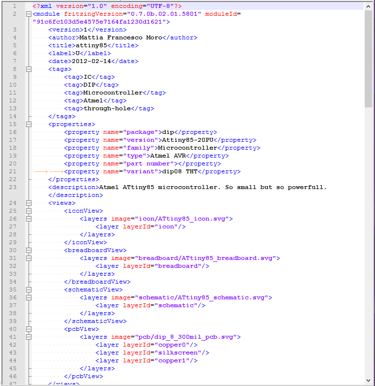
bins/ #Seems like binary files go here?
      #two .fzb's inside - what are those?
----more/ #Icons in PNG and .fzb's.
          #Something about libraries?
contrib/ #Empty in stock install.
         #Probably for whatever libs you download.
core/ # a lot of .fzp's - "Fritzing parts"? Seems so!
Didn't even need to scroll far to see a part named ATtiny85.fzp. Look inside:
![]()
XML. Not a bad choice here, though JSON would take less space - but it works pretty well and is very readable. However, the SVGs are XML and using XML and JSON in one app heavily is likely a clusterfuck. The space hog is the SVGs anyway (they take 125MB in stock install, and another 131MB is Git history).
![]()
![]()
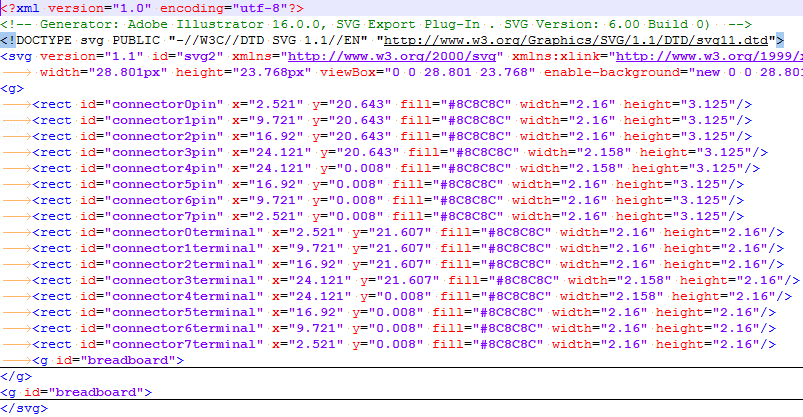
So, parts make heavy use of SVG layers and IDs. Wonder how usable it will be in Inkscape...
The paths shown in svg seem to start from fritzing-parts/svg/core. Let's see those and determine how hard it's to make a part from scratch and where it could be optimized. First, the breadboard view:
![]()
A little bit of pulling layers apart and ungrouping:
![]()
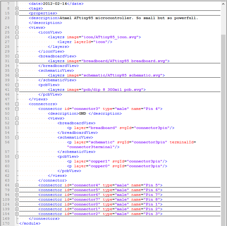
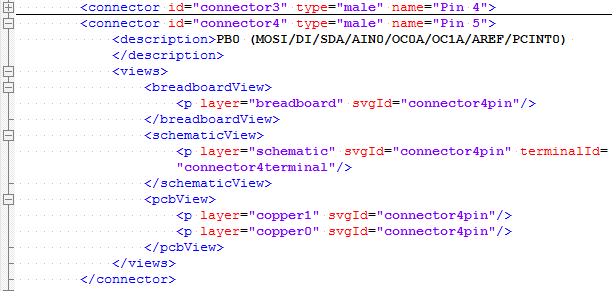
The thing selected is the #breadboard SVG object, as you can see in the upper right. Wonder if that's "layerId" from the breadboardView -> layers -> layer (in SVG excerpt just above), I'm not in the mood for testing (Fritzing loads slowly) and will just assume it is. What else is mentioned out of SVG elements? Connectors, that is - pins!
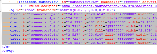
![]()
![]()
![]()
Funny how the connector4terminal is there, but only mentioned in schematic view. Now, the SVG source:
![]()
![]()
I get it, this is autogenerated, but duplicate IDs aren't really the best idea ever. If you look through the file, not only "breadboard" ID is duplicated, but the "connectorXpin" are too. If it's interpreted how I figure it should be interpreted... Let's see.
IDs in .fzp:
- breadboard
- connectorXpin
Additional IDs in SVG:
- connectorXterminal
- Duplicate "breadboard"
- icon
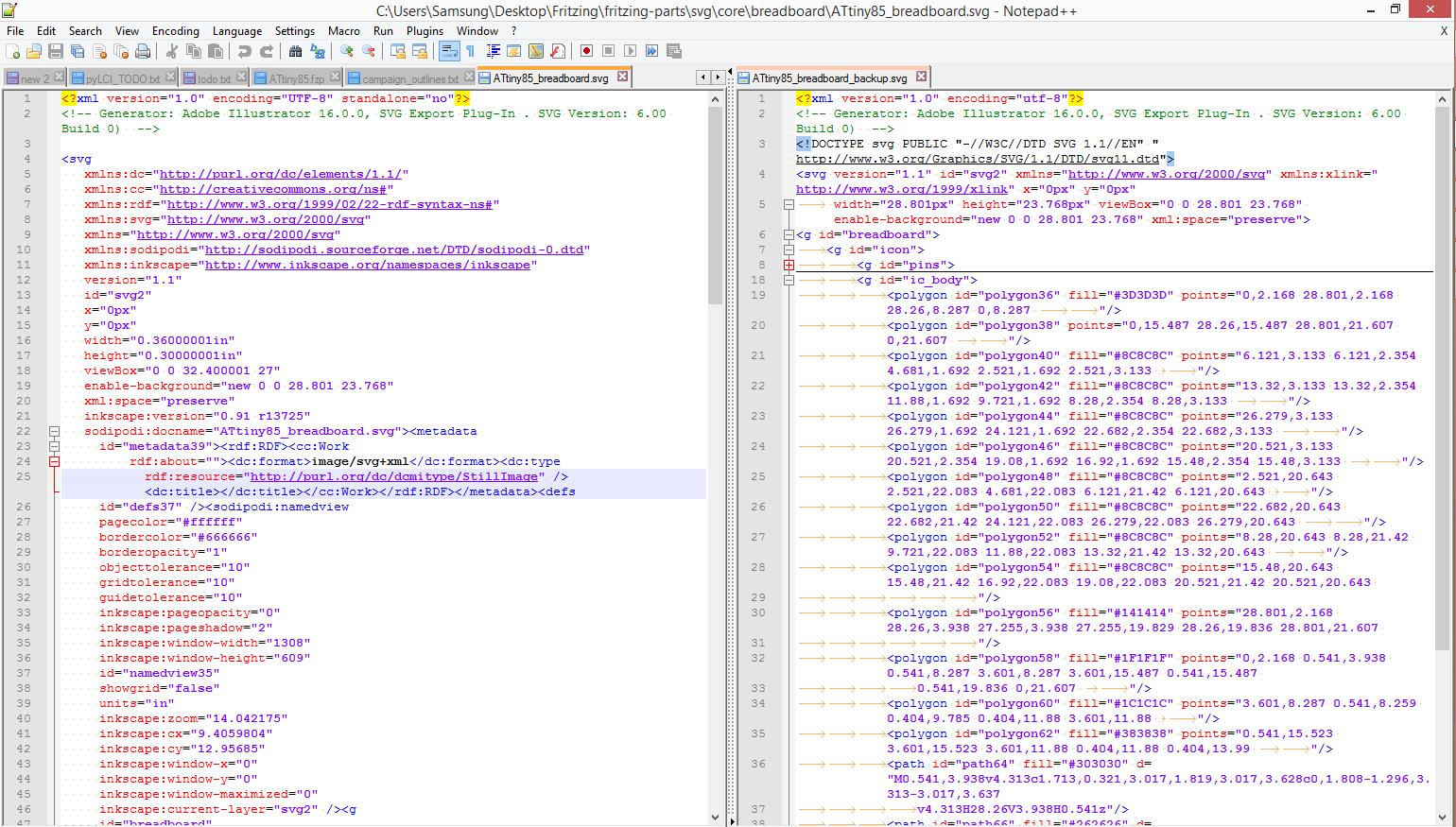
That's it. Let's fix the .SVG by removing all the useless things - it's a little hard because I don't know what's useful and what's not. Thankfully, workflow is simple - editing the SVG in Notepad++ and reloading the Inkscape view:
![]()
![]()
Will not describe the entire process - too much talking for 15 minutes of work
Editing SVGs manually, what could go wrong?
![]()
After this, I started making more granular changes and eventually got there.
End result:
![]()
Redundant tags are there just for readability. Though, come to think of it, that outer <g> is not needed - removed.
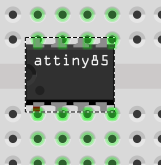
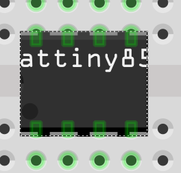
It looks alright in Inkscape, let's put an ATtiny85 on a breadboard in Fritzing... Crap, it looks the same. How do I know it's changed? Let's color pin 1 red:
![]()
Seems like that to test the changes in SVG, it's sufficient to delete the component and place it again. Nice! Footprint works, and there are no duplicate IDs/graphics, and half as much SVG lines.
So, bare minimum should be:
<g id="breadboard">
	<g id="icon">
		<g id="pins">
			<rect id="connector0pin" x="2.521" y="20.643" fill="#FF0000" width="2.16" height="3.125"/>
			...
			<rect id="connector7pin" x="2.521" y="0.008" fill="#8C8C8C" width="2.16" height="3.125"/>
		</g>
		<g id="ic_body">
			<!-- Polygons for graphical IC representation -->
		</g>
	</g>
	<g id="ic_text">
		<!-- IC name layer -->
	</g>
</g>
Oh, and all the header cruft.
Next step? Drawing the simple outline with all the pins in Inkscape!
Thoughts:
- It could be possible to reuse breadboard footprints by having a PCB body layer in one file and IC name layer in another file then combining them somehow. I feel like there's a way to do this already, but don't have a clue yet - maybe I will look into that.
Fritzing: creating your own part
A 3 minute guide, as well as a "from scratch" guide

 Draw grey rectangles. Height is 0.035 as we defined in the beginning, width is about the same, better if it's an even number - like 0.04. Y coordinate is simple to determine - just vertical align top pins to top canvas line, and bottom pins to bottom canvas line. X coordinate calculation:
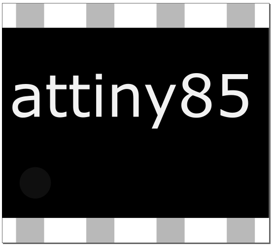


 Well, maybe I can actually learn something from the existing parts, especially provided there are so many DIP-8 ICs shipped with Fritzing. I'm creating everything from scratch, but this saves my frustration for me and time for readers.