-
Part 4: Working software
02/26/2023 at 02:22 • 0 commentsMore progress writing the driver software. TL;DR: Arduino IDE is pants, rewrote it in AVR Assembly.
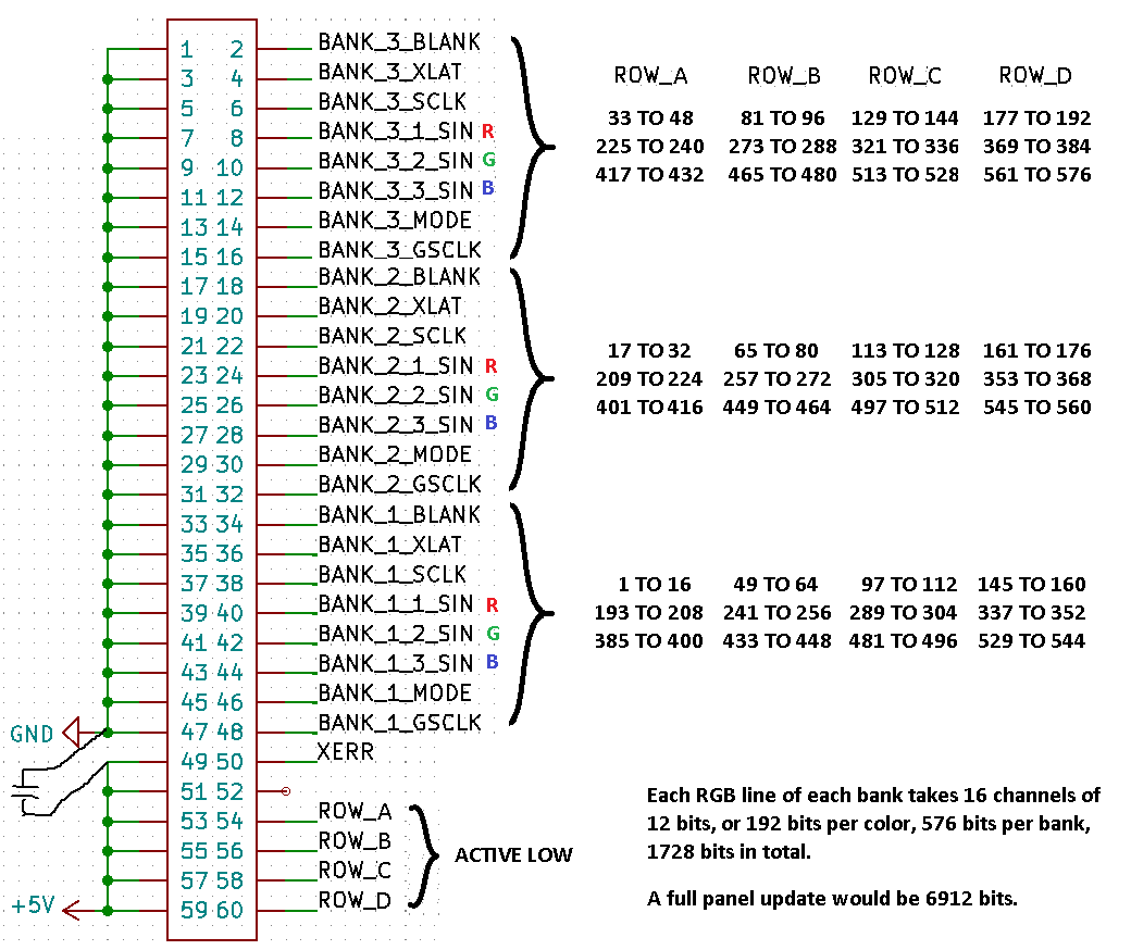
First let's talk about the strategy to run four panels from a single atMega2560 MCU. I decided that to minimize processing, and thus maximize speed, I should do some pre-processing of the image data and pack the bits in a way that's efficient to output. To whit, I gathered all of the IO lines from four panels and packed them into the available outputs on the Arduino Mega 2560:
This scheme was alluded to in the previous log with the sample source code. a standard 24-bit bitmap has one byte for R,G and B values in groups for each pixel. Preprocessing the image data separates the RGB values, and then repacks the bits such that the first byte of the output contains the first bit of the R, G and B streams. Each byte of output is equated to one port per the above image.
Further, the order of the pixels is accounted for: The pixels are sampled starting at row 12, column 16, and across the row to column 1. On the LED panel this maps to (assuming Bank 1):
L400, L399 [...] L385. L208, L207 [...] L193, L16, L17 [...] L1
The data stream for the entire 48x48 display is therefore 5 bytes wide (using 5 ports on the MCU) by 48*8 long; a total of 1920 bytes. Per row. When we account for there being four rows, that's 7680 bytes to fully define the 48x48 pixel image. Luckily the atMega2560 has 8192 bytes of SRAM, meaning we can stuff one full frame of image data into the faster SRAM space with a few hundred bytes left over for things like stack space. Yay!
Now for those paying attention, you might recall that the drivers use 36 bits per pixel - 12 each per color - but we're only sending 24? We do this by padding extra bits, as zeros, to the beginning of the data. This reduces the maximum brightness without messing with the original image data, which is perfectly fine because these things are CRAZY bright at full power and run quite hot to boot, so this reduction makes it much more appropriate for use as, say, a wall display.The preprocessor is written in VisualBasic6 because that's how I roll. The output is a *.asm file that simply gets included at compile time, and one of the first things the CPU does is copy it from program memory into SRAM.
Enough rambling, let's get to some code! Everything is written for AtmelStudio 7, which is now known as Microchip Studio. I've not used the new IDE but I'm sure it's fine.
The main.asm and imgData.asm files are available for download through this project. There is a copious amount of comments explaining what each and every instruction is doing, which is essentially identical to the sample code in the Part 3 project log.
While I wait for the bits I need to clean up this nightmare of wiring (which causes TONS of problems with signal noise, BTW...) the next step is to find a way to mount these panels to a frame along with all the gubbins.
-
Part 3: Some hardware and software
02/19/2023 at 03:45 • 0 commentsBeen plugging away at it, and while the Arduino Mega I decided to use is barely up to the task, it can be hacked to be good enough. Here's some preliminary driver code and the hardware hacks required to get it running.
First the software.
#define CTRLPINS   PORTA            // Port A used for all the control signals
#define CTRLPOUTS  PINA             // Easier and faster to read port state than keep a local variable
#define Data1      PORTC            // Port C is for the RGB data

#define DDCTRLPINS DDRA             // Data direction settings. Change these
#define DDData1    DDRC             // to patch ports above

uint8_t UPDATE;                     // Flag to check if data is ready for update
uint8_t ROW;                        // Keeps track of the row we're updating

void setup() {
  noInterrupts();                   // Disable interrupts while we set things up

  DDCTRLPINS = 0xFF;                // Set data direction to "output" by setting these registers
  DDData1   = 0xFF;

  ROW = 0b00001110;                 // Rows are active LOW so 00001110 = Row 0 active
  UPDATE = 0;                       // Clear UPDATE flag

  // Set up timer/counter. Refer to ATMega datasheet section 17.11.1
  TCCR1A = 0;                       // Reset Timer1 control Register A
  bitClear(TCCR1B, WGM13);          // Set CTC (Clear Timer on Compare) mode
  bitSet(TCCR1B, WGM12);
  bitSet(TCCR1B, CS12);             // Set clock source to T1 (pin 31 of the MCU, NOT Arduino board!)
  bitSet(TCCR1B, CS11);             // This pin is not connected to anything on the Arduino Mega 2560
  bitSet(TCCR1B, CS10);             // So to use it you'll have to solder your own bodge wire

  TCNT1 = 0;                        // Reset Timer1 to known state
  OCR1A = 4096;                     // Set compare value. Interrupt will trigger when counter reaches this value

  bitSet(TIMSK1, OCIE1A);           // Enable Timer1 compare interrupt

  interrupts();                     // Enable interrupts again
}
The above clip is the setup, written in the Arduino IDE so I use some Arduino wrapper functions because speed isn't critical here.
The strategy is to use the 16MHz system clock, divide it by 4 (down to 4MHz) externally and use that for our PWM clock source. We will then feed that 4MHz clock back into the MCU to make a counter go up.
When that counter hits 4096 cycles (the full PWM register value of the TLC5941) it will trigger an interrupt service routine that will reset the PWM counters (setting BLANK to high, then low) and, if all the data for the next update has been clocked in, cycle XLAT and enable the next row of LEDs:
ISR(TIMER1_COMPA_vect)
{
  noInterrupts();                   // Disable interrupts so our interrupt handler isn't interrupted...
  TCNT1 = 0;                        // Reset Timer1 to known state

  CTRLPINS = CTRLPOUTS | BLANK_ON;  // Set BLANK high to disable TLC5941 output and reset PWM counters

  if (UPDATE > 0)                   // If the data has all been shifted in...
  {
   CTRLPINS = CTRLPOUTS | XLAT_ON;  // Pulse XLAT to move TLC5941 input buffers to output registers
   CTRLPINS = CTRLPOUTS & XLAT_OFF;

   UPDATE = 0;                      // Clear update flag

   r = CTRLPOUTS | 0xF0;            // Some jiggery-pokery to quickly update the ROW drivers
   r = r ^ (1 << (ROW+4));          // Probably not the best way but it works
   CTRLPINS = r;

   ROW++;                           // Set the next row
   if(ROW >= 4) ROW=0;              // Don't forget to wrap around
  }

  CTRLPINS = CTRLPOUTS & BLANK_OFF; // Set BLANK low and this enables the output on the TLC5941s

  interrupts();                     // Re-enable interrupts
}
In the roughly 1 millisecond we have between interrupt calls, we can do whatever work we need to do to prepare and shift the new data in. It's perfectly fine that many of the interrupts will only toggle the BLANK line and reset the PWM counters - that's what keeps the lights on. Actual data updates will only occur if all the data has been clocked in as per the UPDATE flag.
void loop()
{
 if (UPDATE > 0) return;            // Skip all this if we're up to date

 /* Whatever image processing needs to be done goes here */

 for (x=0; x<575; x++)
 {
  CData1 = gsData[ROW][x];          // Put serial data on pin.
  CTRLPINS = CTRLPOUTS | SCLK_ON;   // Pulse the SCLK line to clock the bit into the TLC5941s
  CTRLPINS = CTRLPOUTS & SCLK_OFF;
 }

 /*
 In this case, gsData[4][576] is an array of four sets of 576 bytes. Each byte contains
 a single bit of each of the RGB streams: 0b00000BGR

 By doing it this way we can load all three SIN lines with one byte and one instruction.
 This is SUPER fast, which we need to be to keep refresh rates up. We can even drive
 all three sections of the panel using two bytes (9 bits total). For example:
 (Pin is Arduino Mega 2560 board pin)

 Port C
 Bit  Pin  Signal
 ---------------------------
 0    37   Section 1, Red
 1    36   Section 1, Green
 2    35   Section 1, Blue
 3    34   Section 2, Red
 4    33   Section 2, Green
 5    32   Section 2, Blue
 6    31   Section 3, Red
 7    30   Section 3, Green

 Port F
 Bit  Pin  Signal
 ---------------------------
 0    A0   Section 3, Blue
 1    A1
 2    A2
 3    A3
 4    A4
 5    A5
 6    A6
 7    A7

 */

 UPDATE = 1;                        // Set update flag, ready for buffer update!
}
Now, if you read the code comments, it mentions using pin T1 of the ATMega 2560 which is not connected to anything on the Arduino board. In fact if you look at a pinout map of the Arduino Mega 2560, you'll find PD4, PD5, and PD6 are mysteriously absent, along with PE2,PE6, and PE7. These pins exist, but are either reserved for other things or simply not connected for some reason.
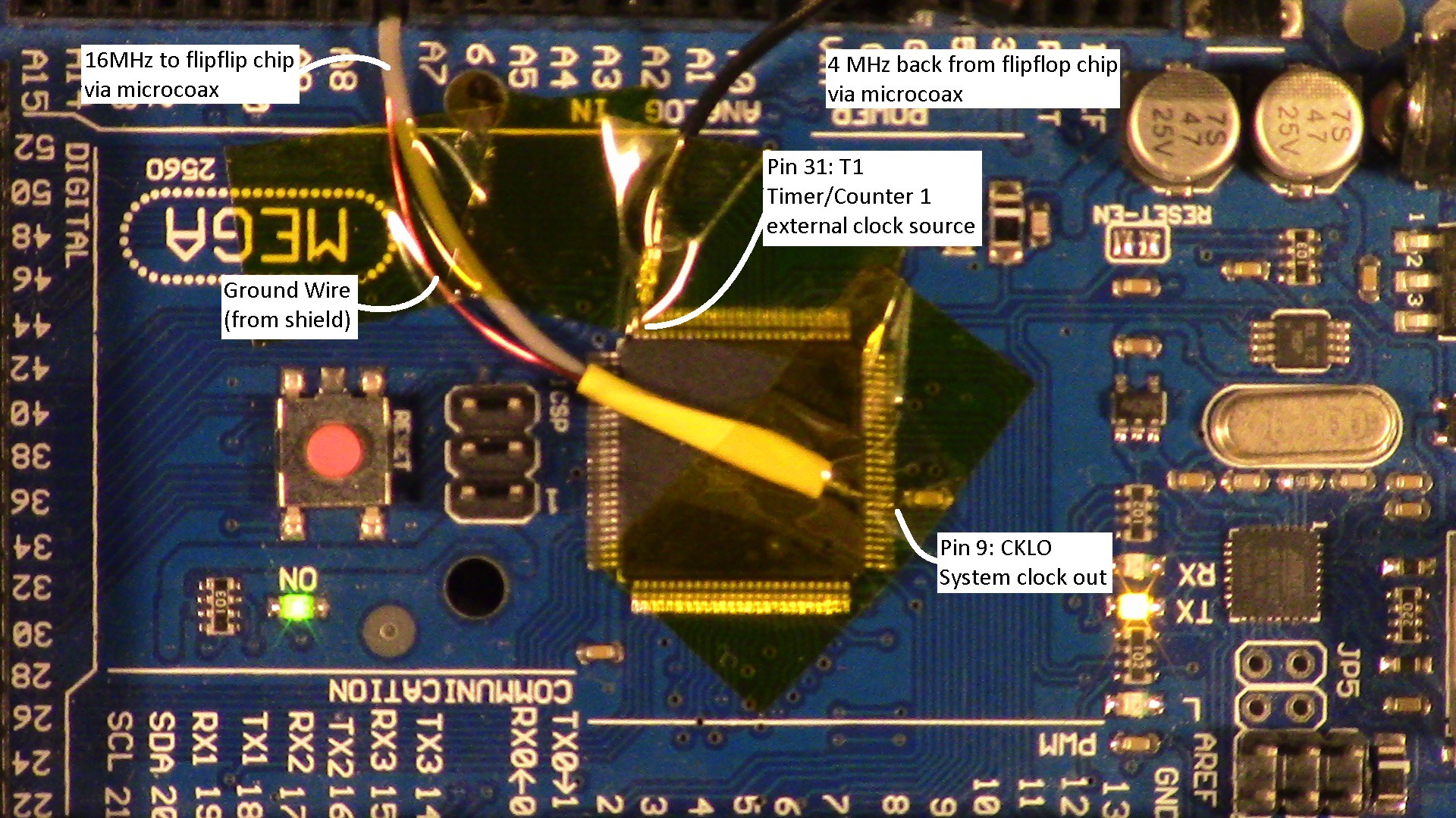
We will need pins PD6 (MCU pin 31) and PE7 (MCU pin 9) for our nefarious purposes, though, so we'll have to get your good eyes out and solder some extra wires;
![]()
To divide the clock by 4, I'm using a SN74F109 I found in a bin of old ICs. This dual J-K flipflip operates up to 25MHz, and feeding the main clock into side 1 and the output of side 1 into side 2, we get a 4MHz signal that we can feed to the TLC5941s as the GSCLK signal as well as the input for our update counter.I'm using some microcoax I salvaged from a dead wifi router in an attempt to control the electrical noise that these clock signals put out. Of course everything is interfaced via cheap breadboard so it's not much help, but maybe when it's all put together properly...
Teeny tiny! This is from an early test to make sure the clock signal was getting out...
Speaking of; By default, CLKO is not active, and there is no signal on pin 9 (unless you write something to port E pin 7). To make this magic happen, we need to reprogram the fuse bits in the Mega 2560 and enable it. To do this, we need to set bit 6 of the Low fuse byte to 0 (default = 1 = pin acts like a normal port pin). I did this by using an Arduino Uno as an ISP and loading up AVRDude in terminal mode (via Windows command prompt:)
avrdude -p m2560 -c avrisp -b 19200 -P COM9 -tChange COM9 to whatever port your ISP is using. Once AVRDude connects without errors or warnings, read the LFUSE byte:
d lfuseBy default, the Arduino Mega 2560 sets the fuses to 0xFF, or 0b11111111. We want to set bit 6 = 0 to enable CLKO, so our new value is 0xBF.
w lfuse 0 0xBFApply and exit, and we're done! Be very careful fiddling with the fuse bits; you can accidentally brick your Arduino if you accidentally, say, set your system clock to an external source and now there's no system clock to program it with. You'll find more information about the LFUSE bits in Table 30-5 of the ATMega Datasheet.
Anyway that's it for this update. Right now it's displaying test patterns at a whopping 120Hz refresh rate and even dimmed LEDs are shimmer-free to both eye and camera!
-
Part 2: Data format
02/08/2023 at 01:56 • 0 commentsWith a better understanding of the physical layout, we can start to figure out how to load bits into this thing to get some blinkenlights happening.
The module is divided into three identical banks, and each bank has separate, identical connections, so we will just focus on a single bank and know we'll have to do everything X3 for get the whole panel working...
The TLC5941 is a 16-channel, 12-bit-per-channel, PWM capable LED driver with dot correction. They can be chained together by linking the serial out (SOUT) of one chip to the serial in (SIN) of the next chip in the chain, and driving the serial clock (SCLK) of all chips in the chain with the same source.
Each of the 16 channels takes 12 bits of data, so fully loading one driver requires clocking in 192 bits. This 12-bit value is used by the PWM control to specify its brightness (0x000 = 0%, 0xFFF = 100%).
Each bank is three groups of three chained-together drivers. Each of these groups is a color channel: Red, Green, and Blue. All three groups share the common control signals but have separate SIN lines. Since there are three chips chained together per group, you will need to clock in 576 bits per color channel to fully define that bank's colors.
Data is shifted into (and out of, via SOUT) the input register. When all of the data is loaded, a signal is given to transfer the input register to the output register, and the output is updated. This lets you clock in new data while the previous data is still being displayed, which reduces glitchyness. Data is clocked in one bit at a time, most significant bit (MSB) first.
The common control lines are:
BLANK: When BLANK is logic high, all outputs are disabled (but the data in the output registers is retained) and the PWM counter is reset. BLANK is pulled high just before the XLAT line is used to transfer data from the input register to the output registers. Resetting the PWM counter is also critical to the operation, and I'll describe that more under GSCLK. Pulling BLANK low will re-enable the output causing whatever data is in the output register to be displayed.
XLAT: Transfer latch. Pulling XLAT high (ideally, while BLANK is also high) will transfer the contents of the input register to the output register. It will also fill the input register with status data, which you can then clock out into your controller, however these modules do not have any connection from the SOUT of the last chip in each chain so getting that signal will require some mod wires.
SCLK: Serial clock. Each pulse of SCLK will shift the input register left by 1 bit, putting the MSB into SOUT and filling the LSB with the state of SIN.
MODE: Programming mode. When MODE is low, SIN and SOUT are connected to the 192-bit input register. When MODE is high, SIN and SOUT are instead connected to a different, 96-bit register (6 bits per channel) that controls the dot correction. Dot correction allows you to set a constant offset for each channel to correct differences in brightness from one LED to the next.
GSCLK: Greyscale clock, aka PWM clock. While the driver has an internal PWM counter, it relies on an externally supplied clock to increment this counter. When BLANK goes high, the PWM counter register is reset. When BLANK goes low, the PWM counter will be incremented by 1 on each rising edge of GSCLK. When the PWM counter matches the input value for each individual channel, that channel output is disabled. The PWM counter must be manually reset by toggling BLANK high then low. Failure to cycle the BLANK signal means the output will get disabled as soon as the PWM counter is up and it wills stay off. In practice, since each channel is 12-bits, you should cycle the BLANK line every 4096 pulses of GSCLK.
Okay, so now that we know what the data lines do, let's discuss how to actually load data and get this thing working...
![]()
Let's say we want to light up LED1 (top left corner) solid RED at 100% brightness. LED 1 is bank 1, row 1A, and we're just worried about the Red channel right now.
First, remember that all of the data is most significant bit first. We will need to load 3 rows worth of data - 576 bits - but the most significant bit is going to be the end of row 3. For bank 1, that will be LED400. LED1's data will be the last 12 bits clocked in.
So we clock in 564 zeroes, and 12 ones, filling channel 0 of chip 1 with 0xFFF.
Now we set BLANK high to temporarily disable the outputs so we can set those outputs without any craziness, and then pulse XLAT to copy the input bits to the output bits. Setting BLANK low again enables the outputs and... nothing!
Well the most obvious thing is obvious: We need to enable the MOSFET for that subrow. We do this by pulling ROW_A (per the above diagram) low. Huzzah! Still nothing!
We will get no output without the GSCLK to drive the PWM controller! So now we start pulsing GSCLCK as slow as we please, or up to 30MHz. One the PWM clock has completed one full cycle, the light comes on! Then immediately goes off again?
The reason it only blinks is because we're not resetting the PWM counter. Once the PWM counter reaches the value of any channel's 12-bit value, that channel is disabled until the PWM counter is reset. We reset it using the BLANK line. So now we have to count 4096 pulses of the GSCLK, pulse the BLANK line, and repeat.
This is a pain in the butt, however it's not like we can't do anything useful during that time; Recall that we need 576 bits to load all of the data into the drivers, so even if SCLK is a quarter the speed of GSCLK, we have enough time to load entirely new values and refresh the display! Don't forget to use XLAT to move the data between registers while BLANK is high!
Ah but there's good reason to want the SCLK the same speed, or faster, than GSCLK: To drive the entire bank - all 16x12 LEDs - we need to load the data for the next sub-row, then switch the MOSFET drives to that sub-row, then set BLANK to low. Now our drive logic looks like this:1 - Clock 576 bits into each of the R, G, and B lines
2 - Set BLANK high
3 - Pulse XLAT to set the data into the outputs
4 - Enable the subrow MOSFET
5 - Set BLANK low to turn LEDs on
6 - Pulse GSCLCK 4096 times
7a - While doing step 6, start with step 1 for the next subrow but do not proceed to step 2 yet.
7b - Once you reach 4096 pulses of GSCLK, continue from step 2
Assuming SCLK and GSCLK are running at the same frequency, you have more than enough time to do all this and even a little bit of time left over for other processing... you'll send 2304 bits of data (thus 2304 SCLK pulses) and 4096 GSCLK pulses per full refresh.
Now multiply all that for banks 2 and 3, and you're driving the whole panel! One caveat though: The MOSFETs control the entire panel, not per-bank, so each bank needs to be updated in synch. Just keep that in mind.
-
Part 1: Physical overview
02/07/2023 at 23:41 • 0 commentsLet's start with a broad overview of what we're dealing with.
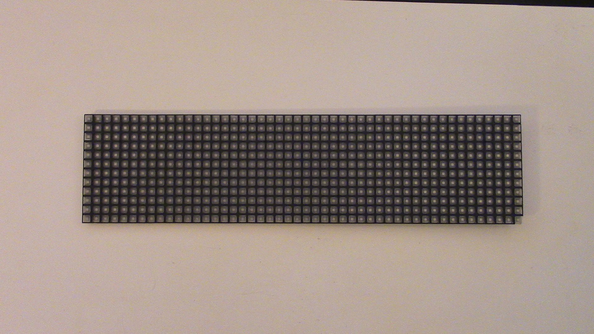
Each board has one one side a 48x12 array of RGB LEDs covered by a multi-part injection molded lens assembly composed of a frosted lens panel and six black grid panels that help visually separate the individual pixel squares. The fact that the black trim bits are 8x12 suggests they made modules of various sizes...
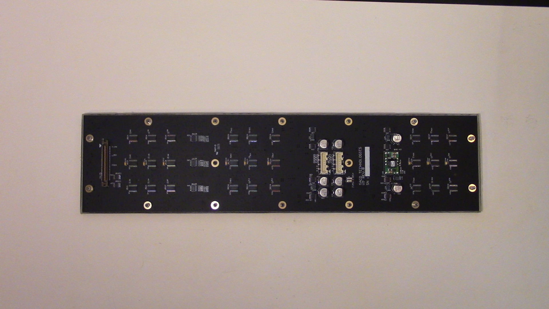
On the back of the board is two power connections, a 60-position main data connector, a step-down converter (as a separate assembly), a bunch of ICs and misc. passives. My boards are stamped "SACO TECHNOLOGIES V9 REV. B." with a field for a hand-written serial number that is blank.
Power connectors are 8-pin, 2.54mm (0.100") pitch, with 4 pins each for +5V and GND. Not able to identify the part number (yet?). All the +5VDC and all the GND pins are connected to each other to form common rails. +5VDC feeds the DC-DC converter, all of the ICs (except the P-channel mosfets), and also connects to the +5V pins of the main data connector. Let this be a warning: It is possible to accidentally power the entire board through the pins on the main connector, which I really doubt are up to the task. In my testing I only connected the GND for common voltage reference and used only the bulk power connectors for the +5VDC supply.
The main data connector looks to be a 3M "Pak 50" series, P50L-060P-AS-DA. The mating connector is P50L-060S-AS-DA. At time of writing, the plug that matches the socket on these boards goes for $10.52 each on Digikey, with a minimum order of 200 and 28 weeks lead time, so we ain't doin' that.
![]()
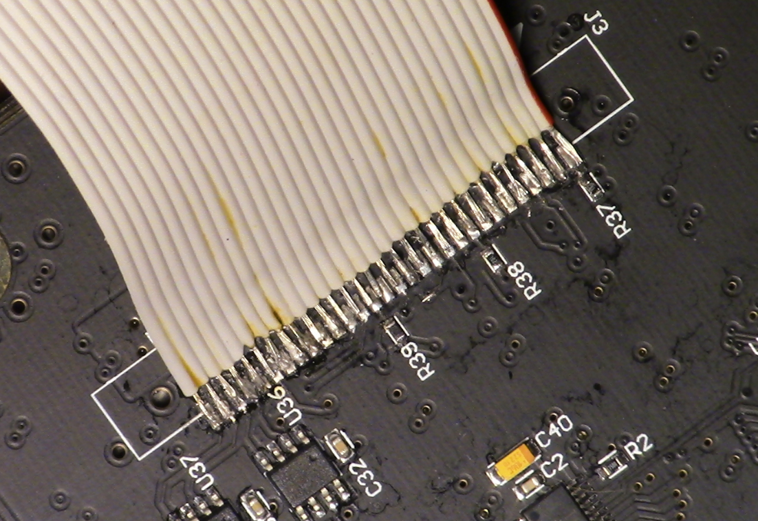
An old floppy drive cable fits the 1.27mm pitch perfectly. This soldering job might not look like much, but it's worth at least $2,104. (and 7 months...)
The power supply module, which steps the 5VDC supply to 3.3VDC, is a PTH05060. This module is rated for an output of 10 amps at a configurable 0.8 to 3.6VDC. As far as I can tell, this 3.3VDC rail is used exclusively for the red LEDs, and all the other LEDs and ICs are supplied by the 5V rail.
The rest of this chips include: LED drivers, octal buffers, mosfet drivers, and dual P-channel mosfets. There are a total of 27 LED drivers, which of course are the key to the whole thing, but let's cover the other ICs briefly.
There are three VHCT541 octal buffer chips, all with their output enable pins tied to ground. 24 of the 28 data pins from the main connector go to these buffers, and since the output is always enabled they immediately pass the input pin state to the output pins. I presume this is done to save the controller from having to source current to drive so many LED driver lines.
Four of the data pins from the main connector go to two dual-channel MOSFET drivers, TC1427C, which of course drive the P-Channel MOSFETs at the other end of the board. Each control input controls 4 of the 16 MOSFETS.
There are eight dual P-Channel MOSFETs. Mine are labeled "D6P02." These are divided into four ICs for the 5VDC rail and and four ICs 3.3VDC rail, but are connected in parallel on their respective rails. That's two MOSFETs per rail per input, and they are in different chips presumably to spread the current out and reduce heat load.
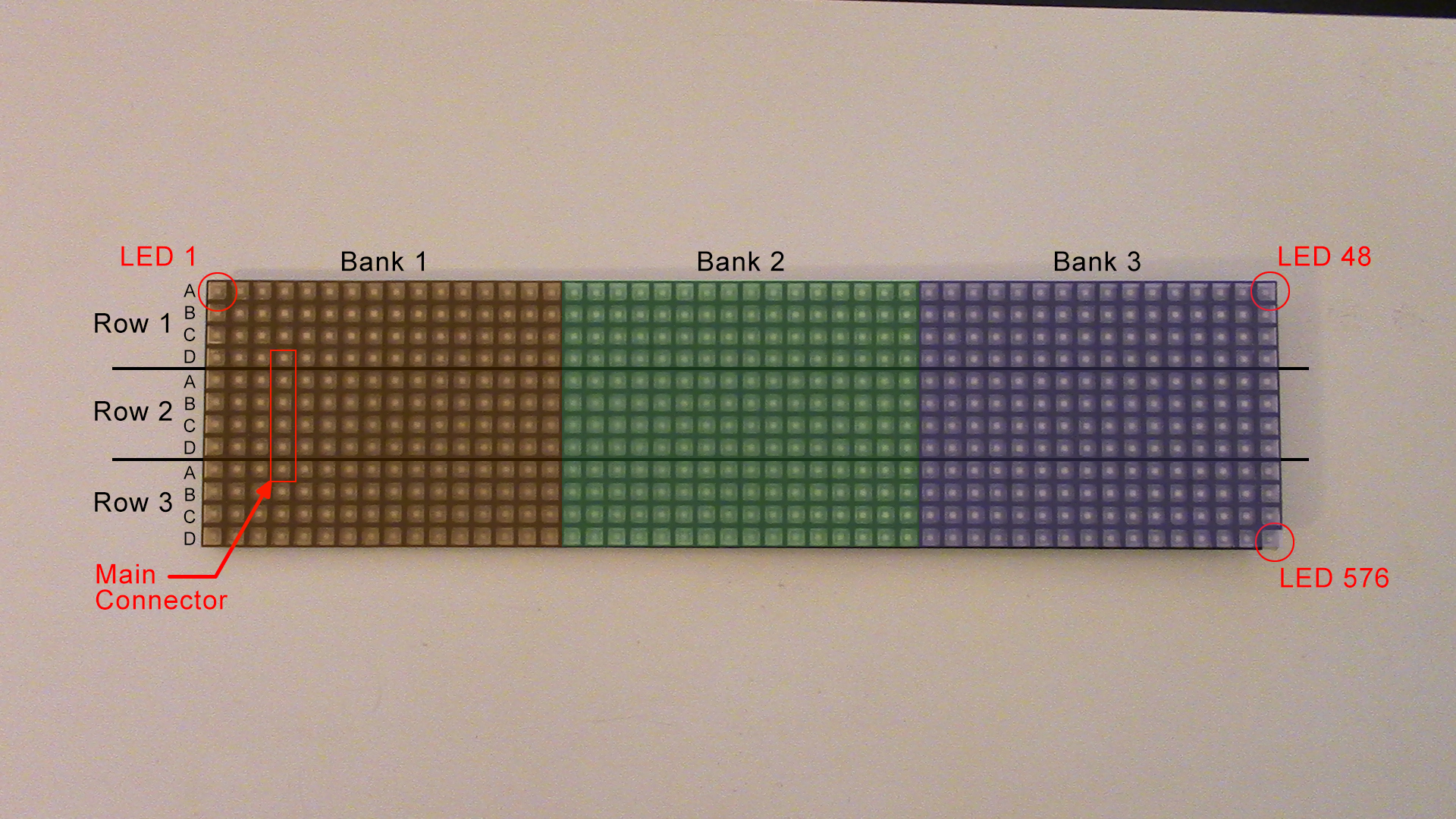
And now the 27 LED drivers; Texas Instruments TLC5941 (Datasheet). These are arranged in three groups that I'll refer to as "banks" in keeping with Huffine's post. Each bank is divided into three "rows," and each row is powered by four power rails each switched separately by the MOSFETs (A,B,C,D)
![]()
9 drivers per bank, 3 per row. Each driver in a row's group of 3 does R,G, and B channels. It's important to note that they are electrically grouped by color, meaning you will need to separate the pixel data by color channel and clock in three rows worth of data for each color, rather than clocking in one row of RGB data.
![]()
A modified and annotated pinout from Huffine's post. They had originally had Banks 1 and 3 reversed, so I changed them around to that LED1 was in Bank 1, Row 1.
That pretty much covers the whirlwind tour of the physical construction, and is more than sufficient to get us started on the main task of figuring out the data format and devising a driver scheme...
(Another) SACO LED Matrix project
There's at least two other project pages for these things, but here I'll document my findings on the actual control scheme and software

