ziggurat29
-
20230216a -- RAM signature stamping
02/19/2023 at 21:20 • 0 commentsRevisiting the RAM signature stamping knowing what I know now, I can better see what's going on and record that knowledge. The RAM stamping routine now looks like this:
F723             ; stamp 'ram valid signature' on RAM page 0 and 3
F723             stampRAMsignature_F723:
F723 18 CE 01 00     ldy     #unk_100
F727 8D 0F           bsr     stampRAMsignatureAtY_F738 ; store ram valid sig @ Y (without nul!)
F729 86 03           ldaa    #3
F72B BD EC 60        jsr     selectRAMPageA_EC60 ; select 32 KiB RAM page as per A
F72E 18 CE 7F DF     ldy     #unk_7FDF
F732 8D 04           bsr     stampRAMsignatureAtY_F738 ; store ram valid sig @ Y (without nul!)
F734 BD EC 79        jsr     selectRAMPage0_EC79 ; select 32 KiB RAM page 0
F737 39              rts
So, the signature is at the beginning of addressable external RAM (XRAM), at 0x0100 on whatever is the current page, and at the end of XRAM at 0x7FDF on page 3. And that's it. There is not checksum over RAM as I had originally guessed. Just these stamped magic values, which happen to be a well-known text string.
This is interesting, because it suggests that page 0 is typically always selected-in. If it wasn't, I would expect that the start of this routine would explicitly do so, perhaps make a note of the current page so as to restore it when done. So this is something to keep in mind: RAM page 0 is possibly always selected in, except as needed.
It is a curiousity as to why the signature starts at 0x7FDF instead of 0x7FE0, since the signature text is 32 bytes and would fit there flush to the end-of-RAM.
A related oddity is in the common 'stamp RAM signature' implementation:
F738             ; store ram valid sig @ Y (without nul!)
F738             stampRAMsignatureAtY_F738:
F738 CE F8 A5        ldx     #aThisIsTheRamVa ; "This is the RAM valid signatur2"
F73B             loop_F73B:
F73B E6 00           ldab    0,x
F73D 27 08           beq     leave_F747
F73F 18 E7 00        stab    0,y
F742 08              inx
F743 18 08           iny
F745 20 F4           bra     loop_F73B
F747             leave_F747:
F747 39              rts
The test at F73D for the nul-terminator is done prior to storing the character, so the signature string is really 31-bytes, since the terminator is not stored although space is allocated for it. So that trailing byte will be a random value.
A further oddity is why the 'e' in signature is changed to a '2', and this may be evidence of some corporate lore we will never know. Conceivably it could serve as a version number such that a RAM image from a prior but incompatible version of the firmware would cause the RAM to be reformatted. However there is no provision for firmware updates. That would only happen in the lab, since you have to open the unit and pull the ROM with a new one you burned. The RAM is battery-backed, so this is a possible occurrence. And this image is firmware version 2.03, so the trailing '2' digit is suggestive of this hypothesis.
But back to the 'random trailing byte'. I would consider this a bug in a code-review, but ultimately it is masked because the signature test implementation also disregards the terminator value:
F6C6             testRAMsignature_F6C6:
F6C6 86 03           ldaa    #3
F6C8 BD EC 60        jsr     selectRAMPageA_EC60 ; select 32 KiB RAM page as per A
F6CB CE F8 A5        ldx     #aThisIsTheRamVa ; "This is the RAM valid signatur2"
F6CE 18 CE 7F DF     ldy     #ramsiglocp3_7FDF ; RAM signature location on page 3 only
F6D2             loop_F6D2:
F6D2 E6 00           ldab    0,x
F6D4 27 0A           beq     next_F6E0
F6D6 18 E1 00        cmpb    0,y
F6D9 26 1F           bne     loc_F6FA
F6DB 18 08           iny
F6DD 08              inx
F6DE 20 F2           bra     loop_F6D2
F6E0             next_F6E0:
F6E0 BD EC 79        jsr     selectRAMPage0_EC79 ; select 32 KiB RAM page 0
F6E3 CE F8 A5        ldx     #aThisIsTheRamVa ; "This is the RAM valid signatur2"
F6E6 18 CE 01 00     ldy     #ramsiglocp0_100 ; RAM signature location on page 0 only
F6EA             loop_F6EA:
F6EA E6 00           ldab    0,x
F6EC 27 0A           beq     leaveSuccess_F6F8
F6EE 18 E1 00        cmpb    0,y
F6F1 26 07           bne     loc_F6FA
F6F3 18 08           iny
F6F5 08              inx
F6F6 20 F2           bra     loop_F6EA
F6F8             leaveSuccess_F6F8:
F6F8 0A              clv
F6F9 39              rts
F6FA             loc_F6FA:
F6FA BD EC 79        jsr     selectRAMPage0_EC79 ; select 32 KiB RAM page 0
F6FD BD F7 54        jsr     setcpLine2_F754 ; set cursor Line 2
F700 CE FC D6        ldx     #aSignatureNotFo ; "(Signature not found. Initializing...)"
F703 BD F6 69        jsr     showText_F669   ; show nts text @ X
F706 BD F7 5A        jsr     setcpLine3_F75A ; set cursor Line 3
F709 86 20           ldaa    #$20 ; ' '
F70B CE 7F DF        ldx     #ramsiglocp3_7FDF ; RAM signature location on page 3 only
F70E             loop_F70E:
F70E E6 00           ldab    0,x
F710 08              inx
F711 36              psha
F712 BD F6 74        jsr     sendLCDbyteB_F674 ; send byte in B to LCD (w/ctrl as per 0x5b)
F715 32              pula
F716 4A              deca
F717 26 F5           bne     loop_F70E
F719 86 02           ldaa    #2
F71B             loc_F71B:
F71B BD F6 1E        jsr     delay590ms_F61E ; delay ~ 590 ms
F71E 4A              deca
F71F 26 FA           bne     loc_F71B
F721 0B              sev
F722 39              rts
with the loop tests at F6D4 and F6EE.
So, I think in sum there are some things that can be asserted about RAM:
- the RAM signature is stamped at the very beginning and end of all RAM, with quirks that are mirrored in the signature test.
- there is no RAM checksum (though comprehensive non-destructive R/W testing can be done through other mechanisms)
- RAM page 0 probably is always selected in, and can hold system variables, except in specific, localized cases.
-
20230215b -- I Got the Power!
02/19/2023 at 14:20 • 0 commentsWhile whizzing through the code I did notice some text:
FCBB 20 20 20 20+aLowBattery:    fcc "             Low Battery!!"
FCBB 20 20 20 20+                fcb 0
referenced at
E514             showLowBattery_E514:
E514 BD F6 18        jsr     clearHomeLCD_F618 ; Clear LCD set cursor pos 0
E517 BD F7 4E        jsr     setcpLine1_F74E ; set cursor Line 1
E51A CE FC BB        ldx     #aLowBattery    ; "             Low Battery!!"
E51D BD F6 69        jsr     showText_F669   ; show nts text @ X
E520 39              rts
in turn referenced at
E503             sub_E503:
E503 12 00 02 0C     brset   PORTA_0 2 locret_E513 ; leave if PORTA b2 high
E507 BD E5 14        jsr     showLowBattery_E514 ; XXX low-battery related
E50A CE 00 04        ldx     #4              ; about 1.96 sec
E50D             loop_E50D:
E50D BD F6 1E        jsr     delay590ms_F61E ; delay ~ 590 ms
E510 09              dex
E511 26 FA           bne     loop_E50D
E513             locret_E513:
E513 39              rts
in turn referenced early in 'start' at
E02E BD E5 03 jsr sub_E503 ; XXX check low battery and show message if neededThe code at E503 is interesting because the whole 'show the low battery message' is only executed if Port A, bit 1 is low. Otherwise it is skipped.
So I conclude that PAb1 is the 'battery OK' indicator. Looking at the board photo, there is clearly a power section to the right, and in particular this device:
![]()
This is a DC-DC converter, and makes since because two AA batteries at nominally 3V is not going to power the 5V system. So it steps up. However, in the datasheet (and I love the '70's disco font used for the section headings), there is a reference circuit on p. 11 for a low-battery indicator, so I suspect that pin 6, A0, of this device is connected to PAb1 of the CPU. (Maybe with some interceding circuitry, but at least logically so.)
-
20230215a -- Keyboard and ISR
02/18/2023 at 17:36 • 4 commentsI had previously thought that ISRs are not materially used, but this turns out to not be strictly true. It is true that most of the ISRs are stubs, but while chasing down all the 8000/C000 references, I found a reference in the maskable interrupt service routine:
E521             isrIRQ_E521:
E521 86 FF           ldaa    #$FF
E523 B7 80 00        staa    $8000  ; set all kbd (high) cols high (inactive)
E526 B7 C0 00        staa    $C000  ; set all kbd (low) cols high (inactive)
E529 3B              rti
Knowing (well, believing at any rate) that 8000/C000 are the keyboard column latches, and in the context of this code:
E406             sub_E406:
E406 14 21 02        bset    TCTL2_21 2      ; TCL2; Edge3 falling edge
E409 14 23 01        bset    TFLG1_23 1      ; TFLG1; IC3 enable
E40C 07              tpa
E40D 84 7F           anda    #$7F            ; clear the 'stop disable' flag
E40F 06              tap
E410 7F 80 00        clr     $8000           ; drive all kbd columns low
E413 7F C0 00        clr     $C000           ; drive all kbd columns low
E416 0E              cli                     ; enable interrupts
E417 CF              stop                    ; place system in low-power mode; waiting for interrupt
E418 01              nop                     ; (can't fiddle with mask bit yet)
E419 0F              sei                     ; disable interrupts for processing
E41A 39              rts                     ; get to it!
It seems that the design is to drive all columns low (normally only one is low at any time during scanning), enable interrupts, then issue a STOP to halt the processor and put it in low power mode. An interrupt will rouse it from sleep, service the interrupt (and raising all the keyboard columns) and resume processing. Resuming means disabling interrupts and carrying on until such time as there is nothing left to do, then returning to this code to park the processor.
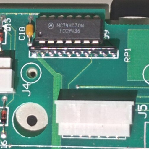
Not exactly interrupt-driven keyboard support, but interrupt assisted. OK, so what is providing the interrupt? My educated guess is the 7430 8-input NAND gate. (You can see it in the top board picture just above the keyboard connector with the row (alternatively column!) connector:
![]()
Recall from a prior post that the keyboard seems to be a garden-variety matrix design, with 16 columns driven by a pair of 74574 octal D, and 8 rows read by a 74573 with pullups. Also these 8 rows feed into a 7430 8-in NAND. So, if /any/ key is down in the selected column ('selected' means a 0 bit on the column line), then one of the row lines will be low, and the NAND will go high. So the 7430 serves as 'there is some key pressed'. And in the context of the sub_E406 setting 8000 and C000 all low (activating all columns) would make any key whatsoever cause a 'keydown detect'. Such a notional 'any keydown detect' causing an interrupt would wake the system, service the interrupt, raising the column lines high, and proceeding with the main loop, which would then perform a proper keyboard scan, dispatching handling as appropriate. So I think we've figured out the main system architecture.
If you examine that closeup, you'll see that pin 8 of the 7430 -- the output pin -- is on the component layer, and you can trace it around in [Eric]'s@EricHertz photo until it tantalizingly disappears between pins 21 and 22 of the CPU, never to be seen again.
![]()
*sigh*. Well, there's other flies in this ointment of a theory, anyway, because the /IRQ lines is active low (or falling edge). The logic of the 7430 as keydown detector is effectively active high. So there would need to be some inversion somewhere. But in the absence of physics, we have philosophy, so I'm holding on to this hypothesis. There's a 7404 inverter nearby (though out-of-the-way for that trace), and a curious transistor looking thing right next to the /IRQ line. If it were a transistor, it could invert. However there are no resistors nearby as would be expected, and moreover the silkscreen indicates 'LV1'. 'Q' is typically used for transistors (and indeed there is a transistor on the other side of the CPU so marked, replete with resistors). So I think this is some other kind of device. It's also next to the /RESET line, so this line of inquiry could be a red herring.
Welp, for now we'll file this mystery away with all the others and motor on.
-
20230214c -- Keyboard, revisited
02/16/2023 at 13:49 • 1 commentOn the trail of the 8000/C000 and bit rotation thing, I found some stuff that looks a lot like keyboard scanning:
E5A0             scanKbd_E5A0:
E5A0 BD E5 90        jsr     sub_E590
E5A3 CC FF FE        ldd     #$FFFE          ; 16-bits, bit 0 low
E5A6 DD 5E           std     word_5E         ; store as (initial) /next/ scan column
E5A8             loopNextKbdCol_E5A8:
E5A8 DC 5E           ldd     word_5E         ; get next scan column
E5AA 1A 83 FF FF     cpd     #$FFFF
E5AE 27 74           beq     loc_E624        ; finished!
E5B0 B7 80 00        staa    $8000           ; XXX keyboard column latch high?
E5B3 F7 C0 00        stab    $C000           ; XXX keyboard column latch low?
E5B6 DD 4E           std     word_4E         ; (save for now)
E5B8 05              lsld                    ; shift up for next scan column
E5B9 CA 01           orab    #1              ; (set the low bit; can only have a single 0)
E5BB DD 5E           std     word_5E         ; save /next/ scan column
E5BD DC 4E           ldd     word_4E         ; (restore /this/ scan column)
E5BF 88 FF           eora    #$FF            ; (invert bits to have 1 in current column)
E5C1 C8 FF           eorb    #$FF
E5C3 DD 4E           std     word_4E         ; remember /this/ scan column; 'rectus'
E5C5 8F              xgdx                    ; get 'rectus' scan column in X
E5C6 F6 80 00        ldab    $8000           ; XXX read keyboard row latch into B???
E5C9 C8 FF           eorb    #$FF            ; complement to rectus row scan mask (1 in row keydown position)
E5CB 8C 80 00        cpx     #$8000
E5CE 27 5C           beq     handleCol15_E62C ; XXX ??? special handle column 15
E5D0 8C 02 00        cpx     #$200
E5D3 27 71           beq     handleCol9_E646 ; XXX ??? special handle column 9
E5D5 8C 01 00        cpx     #$100
E5D8 27 5F           beq     handleCol8_E639 ; XXX ??? special handle column 8
E5DA 8C 00 40        cpx     #$40
E5DD 27 76           beq     handleCol5_E655 ; XXX ??? special handle column 5
E5DF             loc_E5DF:
E5DF 37              pshb                    ; (save row scan mask)
E5E0 BD F5 7B        jsr     sub_F57B
The routine starts with a bit pattern FFFE -- one zero at b0. Then this 16 bit pattern is put out on 8000/C000, shifting up for the next iteration of the loop. The value at 8000 is read. In both cases, the values are 'active low', and inversion is done to make it 'active high'. The 'active high' versions are later passed to routines to convert to a bit number. The process continues until all bits for a given column are consumed, and all columns have been iterated.
The default processing is at loc_E5DF, and consists of translating the column and row scan patterns to column and row numbers, and combining them into an 8-bit value which I call a 'scan code' with row number in the high nybble and column number in the low nybble. These get pushed into a 16-byte buffer at 0x90, with a pull index at 0x8e and push index at 0xef. The enqueue routine is at enqueueKbdScanCode_EBD7, and the dequeue routine is at dequeueKbdScanCode_EBEE.
Since these are scan codes, not ASCII, studying the reference to 'dequeue' will be interesting because it will give us some clues to the key matrix. Most of the keystrokes do have to convert to ASCII. The functional ones might be processed directly as scan codes, though, which will be trickier to puzzle out.
There's some special handling for columns 15, 9, 8, and 5. I haven't explored these yet, but since they are exception paths, it might provide a clue as to the electrical layout.
-
20230214c -- A Curious Cross-reference
02/16/2023 at 13:47 • 0 commentsAs part of a cleanup pass I decided to whizz through the internal data section (0x40-0xc0) and update whether these are 8- or 16-bit quantities by examining references. If I see a 'ldd' or 'std' then I infer that they are 16-bit. Along the way, a few curiosities appear:
There's a bunch of locations that appear to be 'flags'. However, they aren't typically packed bitfields, despite being capable of such. A bit of a waste of space, but I suppose there was space to be wasted in this minimal product.
One thing that caught my eye was location 0x5e. From the cross references I see a 'rol' instruction:
Address           Text
-------           ----
sub_E5A0+6        std     unk_5E
sub_E5A0:loc_E5A8 ldd     unk_5E
sub_E5A0+1B       std     unk_5E
sub_E6BD+11C      ldd     unk_5E
sub_E6BD+128      ldaa    unk_5E
sub_E6BD+151      ldaa    unk_5E
sub_E6BD+16F      ldaa    unk_5E
sub_E84F+3        clr     unk_5E
sub_EA29+49       rol     unk_5E
I'm going to assume this is a 16-bit location for now (it's not uncommon to mess with high/low bytes separately, so I think the 16-bit assumption prevails. For now.)
The first routine in the list is interesting:
E5A0             sub_E5A0:
E5A0 BD E5 90        jsr     sub_E590
E5A3 CC FF FE        ldd     #$FFFE          ; 16-bits, bit 0 low
E5A6 DD 5E           std     unk_5E
E5A8             loc_E5A8:
E5A8 DC 5E           ldd     unk_5E
E5AA 1A 83 FF FF     cpd     #$FFFF
E5AE 27 74           beq     loc_E624
E5B0 B7 80 00        staa    $8000
E5B3 F7 C0 00        stab    $C000
...
The thing that is interesting to me about this is that the value starts with a single 0 bit, is 16-bits long, and the high byte is written to 8000 and the low value written to C000. As mentioned before, I'm pretty sure that is not RAM and is likely memory-mapped stuff. This device is pretty simple electronically, and I know there are two 74374 latches to make 16 keyboard columns. The 'rol' reference to 5E would be involved in walking the bit through a scanning process. And the subsequent byte 0x5f also has a rol reference.
All of this is suggestive that 8000 is the 'high' latch and C000 is the 'low' latch. I don't have the physical hardware, but I'd wager that buzzing out the 74138 would show that it does decode addresses going to those external parts consistent with this mapping.
But what about bit 2 of 8000 and the LCD? I think it is fine for it to serve double duty. Having that line toggle while doing keyboard things won't affect the LCD because it is is not being selected via the PAb7 EX line. And maybe there are other things serving a similar double duty. As mentioned, I don't know where the output lines for the keyboard emulation come from. Maybe here on different bits.
What's also interesting is that 8000 is usually written, but one and one time only read. C000 is only ever written, never read. This suggests that 8000 might also serve as the 74573 keyboard row register.
All this is hypothesis, based on reason rather than measured facts. But intriguing....
-
20230214b -- LCD revisited
02/16/2023 at 13:44 • 0 commentsThe LCD analysis isn't strictly complete. While I'm pretty sure I found the data lines (nybble mode, PD5-2), there are control lines as well.
While rummaging through the RAM stuff, I came across a routine:
F618             sub_F618:
F618 86 01           ldaa    #1
F61A BD F6 5E        jsr     sub_F65E
F61D 39              rts
which then invokes:
F65E             sub_F65E:
F65E 15 5B 02        bclr    byte_5B 2
F661 16              tab
F662 BD F6 74        jsr     sendLCDbyteB_F674 ; send byte in B to LCD (w/ctrl as per 0x5b)
F665 14 5B 02        bset    byte_5B 2
F668 39              rts
before going off to the 'sendLCDbytesB' routine at F674 that I had already reversed. There were some unknowns in that, namely the data location at 0x5B.
I know that the LCD command for "Clear Display and Set Cursor to loc 0" is 0x01, but being a command, it requires that the control lines OC1 and OC2 be set in a particular state. As per doc, here's how they work:
OC2 OC1 function
  0   0 command
  0   1 display address
  1   0 data
  1   1 cursor address
The thing that's interesting here is that we are manipulating byte_5b, which is internal RAM, not a peripheral port. Surely this cannot be memory-mapped. However, revisiting sendLCDbyteB_F674, and the internal routine F68F, it became clear that loc 0x5b stores a virtual copy of those control bits, which then are transferred to harware when writing out the nybble.
F68F             sendLCDnybble_F68F:
F68F 4F              clra                    ; (an elaborate way of A = (0x5b) & 3.  Why? unknown.)
F690 13 5B 02 04     brclr   byte_5B 2 cont_F698 ; LCD control lines state in b1 = IOC2, b0 = IOC1
F694 8A 02           oraa    #2
F696 20 00           bra     *+2             ; delay 3 cy; 1.5 usec
F698             cont_F698:
F698 13 5B 01 04     brclr   byte_5B 1 cont_F6A0 ; LCD control lines state in b1 = IOC2, b0 = IOC1
F69C 8A 01           oraa    #1
F69E 20 00           bra     *+2             ; delay 3 cy; 1.5 usec
F6A0             cont_F6A0:
F6A0 58              aslb                    ; move up two bits to align lower nybble with PDb5-4
F6A1 58              aslb
F6A2 B7 80 00        staa    $8000           ; XXX mystery?
F6A5 96 08           ldaa    PORTD_8         ; PORTD:
F6A7 84 03           anda    #3              ; preserve lower two bits
F6A9 1B              aba                     ; merge on shifted B into nybble position (port D7,6 are not bonded, so who cares about those)
F6AA 97 08           staa    PORTD_8         ; write nybble out
F6AC 14 00 80        bset    PORTA_0 $80 ; 'Ç' ; flick PA7 high, low
F6AF 15 00 80        bclr    PORTA_0 $80 ; 'Ç'
F6B2 39              rts
So, the nybble to send is in B, it is shifted up to positions to get to Port D bits 5-2, and location 0x5b is translated into the two bits at Port D bits 1 and 0. Those are merged together and written out to Port D. PAb7 is then flicked high/low. This almost certainly means that PAb7 is the LCD 'EX' line as per timing diagrams.
This also means that Port D is fully accounted for as for its pins (b7,6 are not available on this 40 pin DIP), unless they do double duty somehow. It's interesting that Port D is configured for open-drain outputs, though in the photo you can clearly see a resistor pack next to where Port D is on the package, so those are doubtlessly pull-ups.
Knowing this, these actions at the start of lcdInit make now sense:
EC16             lcdInit_EC16:
EC16 15 5B 01        bclr    byte_5B 1       ; IOC1, 2 low for 'command'
EC19 15 5B 02        bclr    byte_5B 2
...
Studying other use cases and correlating with datasheet show that 0x5b bit 1 is IOC2 and bit 0 is IOC2, and that these eventually set PDb1,0.
Another mystery is starting to come to light. The mystery of '8000h'. I have seen several writes to this location of values 0, ffh, 4. (Maybe there are others.) Now that I am pretty sure RAM is at 0100-7fff, then what are these writes (and there is a similar one at C000)? So, maybe memory mapped IO? There is an apparently LCD related routine at EC45:
EC45             sub_EC45:
EC45 86 03           ldaa    #3
EC47 97 09           staa    DDRD_9          ; DDRD: b1, b0 output; others input
EC49 86 04           ldaa    #4
EC4B B7 80 00        staa    $8000
EC4E 14 00 80        bset    PORTA_0 $80     ; PORTA:  b7 high
EC51 96 08           ldaa    PORTD_8         ; PORTD: all data bits
EC53 15 00 80        bclr    PORTA_0 $80     ; PORTA:  b7 low
EC56 14 09 FF        bset    DDRD_9 $FF      ; DDRD:  all pins output
EC59 7F 80 00        clr     $8000
EC5C 15 08 3C        bclr    PORTD_8 $3C     ; PORTD:  b5,4,3,2 low
EC5F 39              rts
It's rarely used: once in 'lcdInit_EC16' and twice in success in 'sendLCDbyteB_F674'. In both cases immediately afterwards bit 5 is tested, and looping happens if it set until it goes low. This bit happens to coincide with the 'BUSY' bit of the LCD status. So I am concluding that sub_EC45 is 'readLCDnybble_EC45'. I do not know 8000 for a fact, but being as it sets bit 2, and this is the only place that the LCD is read from, I am starting to suspect that 8000 is a latch, and bit 2 is wired to the LCD R/~W line (and maybe other things!).
So, on-chip port hardware is so far mapping out like this:
Port A:
b7  LCD EX
b6  (not bonded on DIP40)
b5  RAM Bank Select 1 (A16)
b4  (not bonded on DIP40)
b3  RAM Bank Select 0 (A15)
b2  ???
b1  ???
b0  ???

Port D:
b7  (not available with external memory)
b6  (not available with external memory)
b5  LCD data 7
b4  LCD data 6
b3  LCD data 5
b2  LCD data 4
b1  LCD OC2
b0  LCD OC1

Port B, C -- (used for external memory address/data bus)
There's still the possibility of multiple duty for these lines, but these applications at least I think I am pretty confident of.
A pending mystery is the emulated keyboard ports. There are three lines on A unaccounted for, and maybe they're involved with that, but a peculiarity of Port A on this device is that bit 2,1,0 are hard configured in silicon as inputs only. 3 and 7 are bidirectional, but are here configured as outputs (and 5 is hard configured as output). There almost surely needs to be some other output line for keyboard data, so there's more mysteries to solve there, eventually.
Update labels, comments, and propagate....
-
20230214a -- Memory, cont.
02/16/2023 at 13:38 • 0 commentsOperating under the current assumption that RAM is 32 KiB banked at address 0000-7fff, with the first 256 bytes masked off by special function registers and internal SRAM, some other code sections of interest were found. E.g.:
ED00             loc_ED00:
ED00 BD EC 79        jsr     EC79            ; select page 0
ED03 4F              clra
ED04 B7 01 5E        staa    byte_15E        ; ??? stamp page no 0
ED07 86 01           ldaa    #1
ED09 BD EC 60        jsr     EC60            ; select page 1
ED0C 86 01           ldaa    #1
ED0E B7 01 5E        staa    byte_15E        ; ??? stamp page no 1
ED11 86 02           ldaa    #2
ED13 BD EC 60        jsr     EC60            ; select page 2
ED16 86 02           ldaa    #2
ED18 B7 01 5E        staa    byte_15E        ; ??? stamp page no 2
ED1B 86 03           ldaa    #3
ED1D BD EC 60        jsr     EC60            ; select page 3
ED20 86 03           ldaa    #3
ED22 B7 01 5E        staa    byte_15E        ; ??? stamp page no 3
ED25 BD EC 79        jsr     EC79            ; select page 0
ED28 B6 01 5E        ldaa    byte_15E        ; ??? retrieve page number
ED2B 81 00           cmpa    #0              ; validate page no 0
ED2D 26 CE           bne     ECFD
...
So, assuming the 'select RAM page number' functions from yesterday are indeed what they are, it seems that we iterate through the 4 pages, stamping the page number in a well-known location.
Also, following down that path to the ECFD section:
EDDF             loc_EDDF:
EDDF E6 00           ldab    0,x
EDE1 37              pshb
EDE2 36              psha
EDE3 3C              pshx
EDE4 BD F7 48        jsr     setcpLine0_F748 ; set cursor Line 0
EDE7 CE FC A3        ldx     #aAdrbusramErr  ; "AdrBusRAM err:"
EDEA BD F6 69        jsr     showText_F669   ; show nts text @ X
EDED 20 C5           bra     loc_EDB4
...
and then
EDB4             loc_EDB4:
EDB4 38              pulx
EDB5 8F              xgdx
EDB6 BD F5 B0        jsr     showHexAB_F5B0  ; send AB as four-digit hex to display
EDB9
EDB9             loc_EDB9:
EDB9 CE FC B6        ldx     #aExp           ; "Exp:"
EDBC BD F6 69        jsr     showText_F669   ; show nts text @ X
EDBF 32              pula
EDC0 BD F5 B9        jsr     showHexA_F5B9   ; send A as two-digit hex to display
EDC3 CE FC B2        ldx     #aRd            ; "Rd:"
EDC6 BD F6 69        jsr     showText_F669   ; show nts text @ X
EDC9 32              pula
EDCA BD F5 B9        jsr     showHexA_F5B9   ; send A as two-digit hex to display
EDCD 0B              sev
EDCE 39              rts
So, when the stamped page number does not match the selected page, a message is emitted:
AdrBusRAM err: AAAA Exp: EE Rd: RR
and the V flag is set to indicate error
AAAA is the address of the fault (015e), EE is the value expected (the page no), and RR is the value actually read.
OK, so comments added and labels updated and propagated throughout. After that comes some calls to this routine:
EDEF             EDEF:
EDEF CE 7F FF        ldx     #$7FFF          ; start from top of external RAM
EDF2             loop_EDF2:
EDF2 E6 00           ldab    0,x             ; save what's currently there
EDF4 A7 00           staa    0,x             ; stick in our pattern
EDF6 A1 00           cmpa    0,x             ; read back to test
EDF8 26 0A           bne     leaveFail_EE04  ; oh no...
EDFA E7 00           stab    0,x             ; restore what was there before
EDFC 09              dex                     ; next!
EDFD 8C 01 00        cpx     #$100           ; go to bottom of external RAM
EE00 24 F0           bcc     loop_EDF2
EE02 0A              clv                     ; clear V; success!
EE03 39              rts
EE04             leaveFail_EE04:
EE04 E6 00           ldab    0,x             ; fail; save fail address in D for later display
EE06 0B              sev                     ; set V; fail :(
EE07 39              rts
So this fills RAM (non-destructively) with a value in A and tests that it reads back correctly. It goes from 7fff down to 0100, so this also tends to confirm the 'we threw away the first 256 bytes of each page in the interest of simplifying the hardware design' hypothesis.
All this tends to confirm that the external RAM is grouped into 4 x 32 KiB pages, or we'd probably have seen many more page selects made. (Plus there were only two bits in the presumed page select functions, so there can only be four.)
This seems obvious since I've spelled the conclusions out here, but when reverse-engineering a disassembly, you have to be prepared to backtrack any assumptions you make pending future discoveries. But we seem to have a preponderance of evidence in this case, so I feel pretty confident about this interpretation of the RAM arrangement in this system.
-
20230213b -- Memory
02/16/2023 at 13:32 • 0 commentsI find it vexing that I have not yet figured out the RAM banking scheme. Some things:
- at reset, the peripheral configuration registers and internal RAM are mapped at 0000h. They can be moved elsewhere, but are not. The RAM at 40-ff is partitioned into 40-bf is 128 bytes of data, and c0-ff is 64 bytes of stack.
- I can see writes at 0x0100+. Right after that internal memory. It would be a bit of a challenge in external support circuitry to map the external RAM right smack against the internal RAM. Much more sensible would be to map the external RAM to somewhere, say, 4000h, and let from 16 KiB to 48 KiB be a 32 KiB 'page' of RAM in the 128 KiB chip. The decoding logic is easier. (I do not know that the design realizes 32 KiB RAM mappings -- it could be much smaller -- but I am just guessing with this minimal design that less hardware is better, and that is probably the largest power-of-two subdivision of 128 KiB for this 16-bit address space.) But the reads and writes are there nonetheless.
- Could it be that the designers simply chose to 'waste' the first 256 bytes of each page? Because the internal config registers and RAM will be selected in preference to external when ambiguity arises. 256 * 4 = 1024. Maybe they didn't care about wasting 1 KiB of 128 KiB in the interest of making the hardware design cheaper.
- At the same time, the INIT register provides for re-mapping the config regs and also the internal ram elsewhere on a 4 KiB boundary, so those could have simply been moved and then all the RAM would be available. There are 166 padding bytes, so there's code space for a simple setting of that register. On the other hand, moving those registers will make all reference to such 16-bit instead of 8-bit (a privilege of being mapped to the first 256 bytes with special instructions for such accesses). So maybe it was deemed not worth it (or even not possible with the ROM size constraints).
Still, I also see writes to 8000h. If the '32 KiB pages mapped to 0000h' hypothesis holds, then what is going on at 8000h? Mysteries to be solved...
One thing I did find was this code:
EC60             sub_EC60:
EC60 85 01           bita    #1
EC62 26 05           bne     flick3high_EC69
EC64 15 00 08        bclr    PORTA_0 8       ; PA3 low
EC67 20 03           bra     cont_EC6C
EC69             flick3high_EC69:
EC69 14 00 08        bset    PORTA_0 8       ; PA3 high
EC6C             cont_EC6C:
EC6C 85 02           bita    #2
EC6E 26 05           bne     flick5high_EC75
EC70 15 00 20        bclr    PORTA_0 $20 ; ' ' ; PA5 low
EC73 20 03           bra     leave_EC78
EC75             flick5high_EC75:
EC75 14 00 20        bset    PORTA_0 $20 ; ' ' ; PA5 high
EC78             leave_EC78:
EC78 39              rts
This essentially maps bits 1,0 in the A reg into bits 5,3 in the GPIO port A. OK. Well, you have to know a little bit about port A from the manual. Port A has 3 output-only pins, 3 input only pins, and two bidirectional pins. Moreover, two of the pins are not bonded out on this 40-pin DIP device. Bit 5 is output only, Bit 3 is bi-di, but configured for output. Bits 6 and 4 are not bonded.
There are several references to this code, but one of note is at F723:
F723             sub_F723:
F723 18 CE 01 00     ldy     #$100
F727 8D 0F           bsr     sub_F738        ; XXX store 'ram valid sig' @ Y
F729 86 03           ldaa    #3
F72B BD EC 60        jsr     sub_EC60        ; XXX set PA5,3 from A b1,0
F72E 18 CE 7F DF     ldy     #$7FDF
F732 8D 04           bsr     sub_F738        ; XXX store 'ram valid sig' @ Y
F734 BD EC 79        jsr     sub_EC79        ; XXX clear PAb5,3
F737 39              rts
This seems to want to store a textual 'signature' at the beginning and end, assuming that mapped memory cannot access the first 256 bytes (hence the #$100 start). This textual signature ("This is the RAM valid signatur2") is 31 bytes. (32 with nul, but nul is not copied). I don't know why the end starts at 7FDF instead of 7FE0.
But curious to me is that there is the interceding call to sub_EC60 before writing the 'final' signature. Also that there is no effort from an analogous method to set P5,3 into a known state before writing the signature at $100.
This routine is called once during system bootup, and perhaps can make assumptions about the PAb5,3 state as being '00'.
I found another routine:
EC79             sub_EC79:
EC79 15 00 08        bclr    PORTA_0 8       ; clear PAb3
EC7C 15 00 20        bclr    PORTA_0 $20 ; ' ' ; clear PAb5
EC7F 39              rts
Which explicitly sets those pins to '00'. This routine is called quite a bit -- more (17) in fact than the other that selects other pages (12), so I think the system likes to keep the mapping 'parked' at page 0, venturing out to other pages only as-needed.
It's interesting that there is a dedicated 'select page 0' method, when the 'select page A' method would work just fine with 0 in A, but I suspect this is for some flash space economy. There is only 166 free bytes. To replace 17 calls to ones that first clear A and call the general purpose paging routine would rack up more bytes than just calling this routine. (Also, registers are unaffected, so there's some other overhead that might be incurred in using the general purpose routine.)
This ROM is a bit tight for space, and there's some dead code I have found and other opportunities here and there to save some space, but I'm sure no-one is interested in a code review 28 years hence from product launch! It worked well enough at the time...
-
20230213a -- Keyboard Emulation
02/16/2023 at 13:26 • 0 commentsWhile making a clean-up pass (of resolving addresses), I came across a routine at 0xF5ED that prints the message "Attached to Mac, emulating keyboard." or "Attached to PC, emulating keyboard.". Which message is governed by bit 0 in loc 0x008a. I should be able to trace cross references into this function, and to that memory location, to help map out the keyboard emulation code.
Also, creating a data segment for special function registers (SFR) and internal RAM (IRAM)
Tired of scrolling through the datasheet to figure out SFR addresses, I added a data segment 0x0000-0x003f and spent a little time labelling those locations. This is tedious, but it helps a lot because the symbolic names then propagate through the disassembly. Ultimately, I needed to do this for the the IRAM data anyway (and also the external RAM once I figure out where it is mapped), so might as well get started.0000 ?? PORTA_0: rmb 1 0001 ?? rmb 1 ; (reserved) 0002 ?? PIOC_2: rmb 1 0003 ?? PORTC_3: rmb 1 0004 ?? PORTB_4: rmb 1 0005 ?? rmb 1 ; (reserved) 0006 ?? DDRB_6: rmb 1 0007 ?? DDRC_7: rmb 1 0008 ?? PORTD_8: rmb 1 0009 ?? DDRD_9: rmb 1 000A ?? rmb 1 ; (reserved) 000B ?? CFORC_B: rmb 1 000C ?? OC1M_C: rmb 1 000D ?? OC1D_D: rmb 1 000E ?? ?? TCNT_E: rmb 2 0010 ?? ?? TIC1_10: rmb 2 0012 ?? ?? TIC2_12: rmb 2 0014 ?? ?? TIC3_14: rmb 2 0016 ?? ?? TOC1_16: rmb 2 0018 ?? ?? TOC2_18: rmb 2 001A ?? ?? TOC3_1A: rmb 2 001C ?? ?? TOC4_1C: rmb 2 001E ?? ?? TI4O5_1E: rmb 2 0020 ?? TCTL1_20: rmb 1 0021 ?? TCTL2_21: rmb 1 0022 ?? TMSK1_22: rmb 1 0023 ?? TFLG1_23: rmb 1 0024 ?? TMSK2_24: rmb 1 0025 ?? TFLG2_25: rmb 1 0026 ?? PACTL_26: rmb 1 0027 ?? PACNT_27: rmb 1 0028 ?? SPCR_28: rmb 1 0029 ?? SPSR_29: rmb 1 002A ?? SPDR_2A: rmb 1 002B ?? BAUD_2B: rmb 1 002C ?? SCCR1_2C: rmb 1 002D ?? SCCR2_2D: rmb 1 002E ?? SCSR_2E: rmb 1 002F ?? SCDR_2F: rmb 1 0030 ?? ?? ?? ??+ rmb 9 ; (reserved) 0039 ?? OPTION_39: rmb 1 003A ?? COPRST_3A: rmb 1 003B ?? PPROG_2B: rmb 1 003C ?? HPRIO_3C: rmb 1 003D ?? INIT_3D: rmb 1 003E ?? TEST_3E: rmb 1 003F ?? CONFIG_3F: rmb 1Soon I'll start posting the full disassembly for the curious in the files area, but right now I'm moving so fast that it would be wildly out-of-date at any moment.
-
20230212d -- LCD Display
02/15/2023 at 19:45 • 2 commentsThe LCD is a 40x4 character display. Judging by my friend [Eric]'s@EricHertz photos, this is not the common HD44780 device, but instead a Mitusbish M50530
![]()
I did find a datasheet for this device. If it's not code compatible with the '44780, it sure is similar in operation. Perhaps later I'll compare datasheets.
It seems we're operating in 4-bit mode, using Port D bits 5-2 for data. I haven't figured out the other control lines, but PAb7 seems to be the one that strobes the data. There has to be at least one more that controls 'data/instruction'. I found several routines that fiddle with it, and have deduced these things:
This is called once during system boot, just prior to displaying
EC16             lcdInit_EC16:
EC16 15 5B 01        bclr    unk_5B 1
EC19 15 5B 02        bclr    unk_5B 2
EC1C             loop_EC1C:
EC1C BD EC 45        jsr     sub_EC45        ; XXX LCD related??? gpio flicking, PA7 high/low. return PD in A ; $8000 stuff
EC1F 84 20           anda    #$20 ; ' '      ; wait for LCD 'ready'
EC21 26 F9           bne     loop_EC1C
EC23 C6 DB           ldab    #$DB ; '¦'      ; LCD SF:  nybble mode, 5x8 font, 4x40
EC25 BD F6 74        jsr     sendLCDbyte_F674 ; send byte in B to LCD
EC28 C6 50           ldab    #$50 ; 'P'      ; LCD SE:  cursor increments after write, no change in display address start address
EC2A BD F6 74        jsr     sendLCDbyte_F674 ; send byte in B to LCD
EC2D C6 3B           ldab    #$3B ; ';'      ; LCD SD:  Display On, Cursor On, Underline Off, Cursor Blink, Character Blink
EC2F BD F6 74        jsr     sendLCDbyte_F674 ; send byte in B to LCD
EC32 C6 0D           ldab    #$D             ; LCD SU: set/reset mode cancelled
EC34 BD F6 74        jsr     sendLCDbyte_F674 ; send byte in B to LCD
EC37 C6 05           ldab    #5              ; LCD SB: set blink frequency
EC39 BD F6 74        jsr     sendLCDbyte_F674 ; send byte in B to LCD
EC3C C6 01           ldab    #1              ; LCD CH: clear display and home
EC3E BD F6 74        jsr     sendLCDbyte_F674 ; send byte in B to LCD
EC41 14 5B 02        bset    unk_5B 2
EC44 39              rts
I found some others related to sending a byte to the display (used both for commands and data) @ F674, and emitting nul-terminated text @F669, and several 'set cursor position' routines for setting the cursor position at the beginning of each of the 4 lines @ F748, F74E, F754, F75A.
ROM Disassembly - AlphaSmart Pro
Wherein I disassemble the ROM from a vintage typewriter-thing