 zpekic
Running Tiny Basic benchmark program with symbolic tracing.
Please refer to the project logs for in-depth description.
Run-time visualization of memory and I/O space by running tracer component (VHDL) on target and tracer utility (C#) on the host.
Step by step from micro-coded Intel 8080 compatible CPU based on Am2901 slices to small system running Tiny Basic from the Disco Era.
Already have an account? Log in.
To make the experience fit your profile, pick a username and tell us what interests you.
Running Tiny Basic benchmark program with symbolic tracing.
Please refer to the project logs for in-depth description.
Run-time visualization of memory and I/O space by running tracer component (VHDL) on target and tracer utility (C#) on the host.
Visibility into what is exactly going on inside the target machine is crucial for debugging and development. There are few ways to accomplish this:
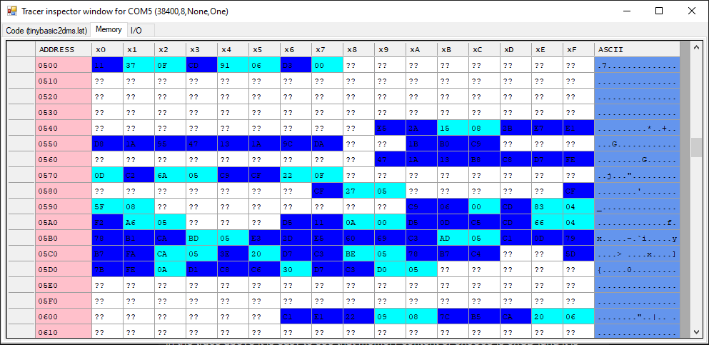
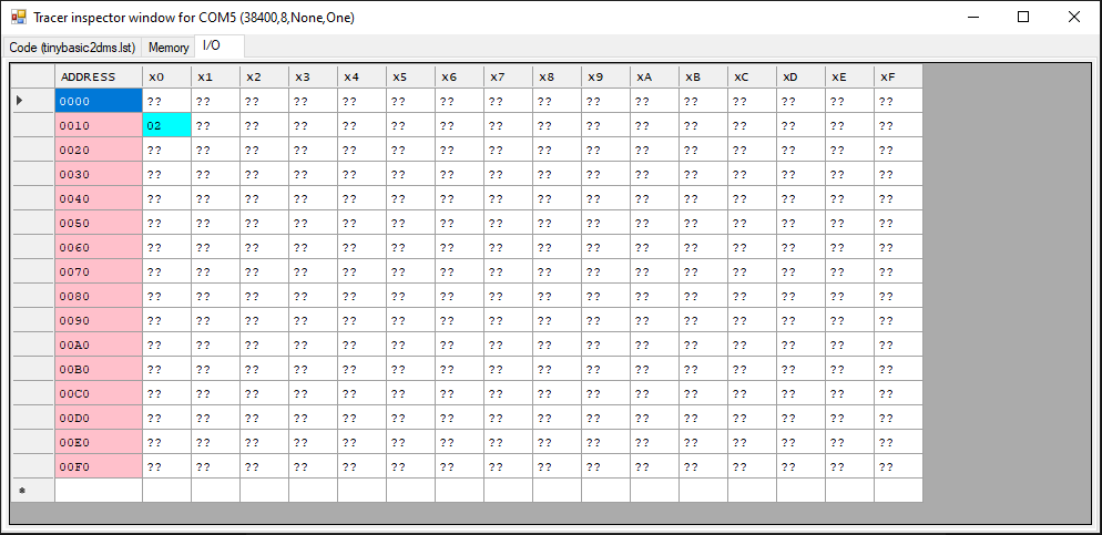
If the tracer is configured to trace each memory access and/or I/O access, given that the trace goes to host, it is possible to store the address and value of such access and as the execution is ongoing create an accurate map of the memory.
In the trace above it is easy to see that memory content of 0x0503 is 0xCD (and it is instruction), and 0x0501 is data memory, content 0x37. Also port 0x10 has value of 0x02 etc.
Mapped onto memory grid which has been added to tracer:
And I/O:
In this sample session, it is easy to observe how and where a Tiny Basic program is stored in the memory, and how it gets there from input buffer when the input line is terminated (Enter key)
There are 3 components that allow the run-time visualization to work:
"debugtracer" component embedded in target device - as described in the other project log, the logic in this component is comparing the state of control signals (M1, /IORD, /IOWR, /MEMRD, /MEMWR) at each CPU clock with the state of 5-bit internal register reg_sel. If any match, this will flip the READY signal low, "freezing" the CPU in the current cycle (actually due to a bug in my design this is done by stopping the clock signal, which would not be possible in read device because 8080-family processors were not static (few were at the time, except the CDP 1802 unique in that regard too).
reg_sel can be loaded from 5 on/off switches on the FPGA baseboard, but this is done when the "load" signal (connected to push button) is asserted. This way one trace configuration can be running while the other is being prepared. With reg_sel cleared, CPU runs at full speed, without traces being sent out.
UART sender - a simple 16-to-1 MUX sends out the ASCII character assembled from data on the bus and template that depends on actual CPU cycle. The operation is as follows:
signal counter: std_logic_vector(7 downto 0);
alias chrSel: std_logic_vector(3 downto 0) is counter(7 downto 4);
alias bitSel: std_logic_vector(3 downto 0) is counter(3 downto 0);Note that the UART is one way only from target device to host, and is completely different serial channel from the bidirectional UART that allows interaction with Basic on the single board microcomputer.
Tracer utility running on the host - The code for this C# utility is here. Let's say that the record received is:
MR,0761 ED<cr><lf>
Upon assembling the record incoming on serial port the record descriptor (memory read == MR) will be detected:
                        case "MR":  // read memory (except M1)
                            if (CheckRecipientAndRecord(memoryMap, recordValue.Split(' '), out address, out data))
                            {
                                CheckLimit(memoryMap.UpdateRead(address, data, ref pause), traceRecord);
                            }
                            Console.ForegroundColor = ConsoleColor.Blue;    // BLUE for not implemented trace record type
                            Console.WriteLine(traceRecord);
                            break;
If the address and data look valid, check limit will validate if the address is within displayable range (64k for memory, 256 for I/O, although restricted in this case to 4k because the SBC has 2k ROM and 2k RAM). Then the memoryMap will be updated to hold the record of read operation:
public bool UpdateRead(int address,...
Read more »
Context
Given that this CPU implementation is an almost canonical example of microcoded design as envisioned by AMD - and a showcase of their Am29XX and Am25XX ICs - it is very helpful to go over at least chapters I and II of the "Bit-slice microprocessor design" book for better understanding. After that, the application note provides a great explanation of this specific CPU implementation. All source files to implement the CPU are under this folder.
(for control unit, which the other major part of the CPU, see this log)
Execution unit
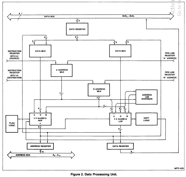
This part of the CPU is where registers (both program accessible AF, BC, DE, HL, PC, SP) and temporary / internal are held, and modified by passing through ALU and other data paths.
The central component of the execution unit is a set of 4 Am2901 bit-slices. This fascinating chip was the de-facto standard during the heyday of the era (1970ies), although Intel, MMI, and Texas Instruments had bit-slices too.
The most important question when designing with bit-slices is how to map the design registers (program accessible and internal only) to the available set of slice registers. Intel 8080 (and 8085) has 6 16-bit program accessible registers so they can be mapped in different ways, for example:
| Mapping --------- (registers 0..15) | Number of slices | Pros | Cons |
| By 8-bit register ---------- B C D E H L M A SP.H SP.L PC.H PC.L ? ? ? ? | 2 | Cost savings! (only 2 slices), fast for 8-bit operations, max register utilization | Slow for 16-bit operations, additional external 16-bit register needed |
| By 16-bit register pair ---------- BC DE HL MA SP PC ?? ?? ?? ?? ?? ?? ?? ?? ?? ?? | 4 | Fast for 16-bit operations, simpler design | 4 slices needed, additional external MUXs and other logic for 8-bit operations, slower for 8-bit operations, many unused registers (could be viable for Z80) |
| Mixed --------- BC CB DE ED HL LH ?A A? ?? SP ?? ?? 0038 3800 ?? PC | 4 | Overall good speed for both 8 and 16-bit operations Note: this approach was adopted by AMD engineers for this design | 4 slices needed, additional external MUXs and other logic |
(for comparison, see the deep dive into real implementation of registers in Intel 8085 which was improved version of 8080)
To see how register mapping works in hardware and microcode, here are 2 examples:
8-bit operation, MOV B, E
Op-code format is 01 ddd sss (B = 000, E = 011) => 01000011 => 043H
Looking up 043H in mapper ROM we find the start address of the microcode routine to implement the operation which is 014H (1 cycle after which there is jump to label HLDF):
;0014 MOVRR: ALU,,,FTOB.F & ALUC & BASW SW,SW & OR & ZA & IOC & /IF R.F, INV,HOLD & NUM, HLDF & NOC
0014 1100000000101111 1010101111110000 0111010101010100 11011100
The action part is 9-bit Am2901 operation (highlighted):
DST = 011 = RAMF
OPR = 011 = OR
SRC = 100 = ZA
Which means, register addressed by 4-bit address A (am2901_a) will be OR'd with 0 (so no change) and deposited to register addressed through B 4-bit address (am2901_b). As the upper 8-bytes are ordered B, C, D, E, it is clear that right 8080 internal register transfer will occur (these bytes are in the HOP = high order part 2 slices):
-- HOP slices ---
	u33: Am2901c port map (
				  clk => CLK,
				  a => am2901_a,
				  b => am2901_b,
				  d => am2901_data(11 downto 8),
				  i(8 downto 6) => pl_alu_destination,
				  i(5 downto 3) => pl_alu_function,
				  i(2 downto 0) => pl_alu_source,
				  c_n => u64_pin4,
				  oe => '0',
				  ram0 => signal_b,
				  ram3 => am2901_ram11,
				  qs0 => signal_a,
				  qs3 => am2901_q11,
				  y => am2901_y(11 downto 8),
				  g_bar => open,
				  p_bar => open,
				  ovr => open,
				  c_n4 => am2901_c11,
				  f_0 => u33pin11,
				  f3 => open,
				  -- DEBUG PORT --
				  debug_regsel => am2901_dbg_sel,
				  debug_regval => am2901_dbg_val(11 downto 8)
	);
But looking at the lower 8-bits, they are reversed (C, B, E, D). That's why in the actual wiring of the processor upper 2 Am2901 slices directly get the A, B fields from microcode or instruction, but lower...
Read more »Context
Given that this CPU implementation is an almost canonical example of microcoded design as envisioned by AMD - and a showcase of their Am29XX and Am25XX ICs - it is very helpful to go over at least chapters I and II of the "Bit-slice microprocessor design" book for better understanding. After that, the application note provides a great explanation of this specific CPU implementation. All source files to implement the CPU are under this folder.
(for execution unit, which the other major part of the CPU, see this log)
Control unit
(for good discussion of these refer to "Bit-Slice Design: Controllers and ALUs" by D. E. White)
The key to micro-coded CPUs/controllers is their control unit. Typically this control unit has a very limited set of instructions it can recognize:
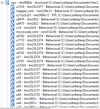
This is how the control unit for Am9080 looks like:
Let's identify and describe each element as defined in the code:
8-bit register with input connected to the D-bus (instructions come always from there, either through memory read, or presented by external hardware as a result to INTA (interrupt acknowledge cycle)
    -- instruction register ---
    u1516: am25ls377 port map (
        clk => CLK,
        nE => pl_instregenable,
        d => DBUS,
        q => current_instruction
    );
current_instruction is the 8-bit opcode of the currently executing machine instruction. Where is the nE (load enable) signal coming from? From microcode instruction which is executed during instruction fetch:
;0004 FETCH: ALU DOUBLE,PC,PC,FTOB.F & OR & ZA & ALUC & BASW & /IOC IN,,TO.A & MEMR & IF ,INV,READY & NUM, $
0004 0100000000010000 0010010111010001 0011011111111110 11011100;
;
;0005 INCPC & IF D.R. ,HOLD & NUM,HLDD & NOC
0005 1100000000110000 1110100111110001 0011011111111110 11000100;
in other words, signal pl_instregenable is microinstruction bit 55 (MSB) and this is the only time when it appears low.
as explained here, this memory is a "many to one" lookup table.
    -- u11, u12, u13 ----------
    mapper_rom: rom256x12 Port map (
        address => current_instruction,
       data => instruction_startaddress(11 downto 0)
   );
For each op-code presented as 8-bit address (current_instruction) a 12-bit data will appear on the output (only 9-bits are of interest as the microprogram memory is 512 words deep). The instruction_startaddress is then presented as one input of the Am2909-12 device:
In original schema these are 3 4-bit Am2909 devices, merged here together:
    -- to save some FPGA area, 3 * 2909 = 1 * 2909-12
    u21u22u23: am2909x12 port map (
        S => sequence(1 downto 0),
        R => u_immediate,
        D => instruction_startaddress,
        ORi => interrupt_or_mask,
        nFE => sequence(3),
        PUP => sequence(2),
        nRE => '0',
        nZERO => nRESET,
        nOE => '0',
        CN => '1',
        CLK => CLK,
        -- Output ports
        Y    => ma,
        C4    => open
    );
Looking inside the Am2909-12, we see that the 12-bit uPC inside the Am2902-12 will be loaded when sequence(3 downto 0) == "1011"
The sequence is coming from another simple lookup table:
   --- sequencer rom ----
    u14: rom32x8 port map ( -- TODO: it is actually 16*5 only
        nCS => '0',
        address(3 downto 1) => pl_nextinstrselect,
        address(0) => u8474_u8475_pin15,
        data(4 downto 0) => sequence
    );
This sequence is marked "D" and the address input must be 0010 (2) to return it:
type rom is array(0 to 15) of std_logic_vector(4 downto 0);
constant lookup: rom := (
            "01000", -- C
            "01001", -- R
            "01011", -- D
            "01001", -- R
            "01000", -- C
            "00101", -- SBR
            "01001", -- R
            "00010", -- RTN
            "11010", -- F
            "00101", -- SBR
            "00000", -- POP
            "00001", -- PR
            "01001", -- R
...
Read more »
(for related subject, run-time initialization of ROMs/RAMs, see here)
FPGA-based designs often have various read-only stores. Their content can be defined in different ways:
Last option was used in this project. There are 3 ROM stores that needed initializing and they have different formats:
Tiny Basic ROM (2k*8)
Assembling Tiny Basic source using zmac assembler produces multiple output files, one of which is in Intel hex format. Given that Xilinx was (and after AMD takeover) remains Intel / Altera competitor, it's freeware ISE 14.7 does not offer direct support for .hex files. However, creating a parser for it is relatively straightforward, esp. if some fancier features (not used in the file that needs to be ingested) are left out. The "magic" is visible in the ROM source code file:
architecture Behavioral of rom1k is

-- function defined in the package pulls in the content of the
-- hex file in generic parameter
constant rom: filemem(0 to (2 ** address_size) - 1) := init_filememory(filename, 2 ** address_size, default_value);
--attribute rom_style : string;
--attribute rom_style of rom : constant is "block";

begin

D <= rom(to_integer(unsigned(A))) when (nOE = '0') else "ZZZZZZZZ";

end Behavioral;
The usual inline ROM initialization similar to (note type is an array fixed in both depth and width dimensions):
type mem16x16 is array(0 to 15) of std_logic_vector(15 downto 0);
constant decode4to16: mem16x16 := (
    "1111111111111110",
    "1111111111111101",
    "1111111111111011",
    "1111111111110111",
    "1111111111101111",
    "1111111111011111",
    "1111111110111111",
    "1111111101111111",
    "1111111011111111",
    "1111110111111111",
    "1111101111111111",
    "1111011111111111",
    "1110111111111111",
    "1101111111111111",
    "1011111111111111",
    "0111111111111111"
);
is replaced by a function call (note array type has variable depth but fixed 1 byte width):
type filemem is array(natural range <>) of std_logic_vector(7 downto 0);

impure function init_filememory(file_name : in string; depth: in integer; default_value: std_logic_vector(7 downto 0)) return filemem;
This function will be invoked during build time, and it will use file_name, 2^address_size and default byte value as parameters to run. The init_filememory() function can be found in the package source file which is included in each project source as needed.
The gist of the function is a line-by-line read of the file referenced in the parameter. The beginning of the record (<colon><bytecount><address><recordtype>) is always the same, and then record type is inspected to be either 00 (data) or 01 (end of file), other types are not supported. Bytes are then parsed from rest of the line (the number of expected hex digits is known) and written to the temporary variable. When whole file is parsed, input file is closed and the temporary variable returned as result of the function call, which creates data structure compatible with the constant ROM definition file.
This build-time initialization works for RAMs too. In that case "constant rom" should be replaced by "signal ram" and code to write content when write and select are asserted added.
The other 2 ROMs that needed initialization are in the CPU itself.
Mapping PROM (256*12)
The contents of this memory is taken directly from the article, and the format is:
<AAAA> <DDD>[;comments]
AAAA, DDD are hex characters to define address (00H-FFH, upper 2 are not used) and data (000H-FFFH). This simple format is easy to parse, and the code is under load_mem() function in the VHDL component file.
load_mem() and dump_mem() are wrapped into common init_wordmemory() function:
constant data_from_file: t_mem256x12 := init_wordmemory("../am9080/prom/mapper.mif", "../am9080/prom/mapper.hex", 256, uPrgAddress_nop);
This way, the...
Read more »Much of the time developing any computer - related project is spent debugging. Hobby projects with FPGAs are no exception, if anything the debugging time is even more as the computer itself is defined in software.
In initial stages, simple LEDs are very useful for basic debugging (e.g. "does PC even increment?", "which microinstruction address is it executing" etc.), and switches and buttons allow for doing this cycle by cycle or at any speed. But at some point, more is needed. Luckily, very custom debugging circuits can be written together with the actual device and tailored to exactly its function.
In this case, a "debugtracer" component was added to the system. Its function is pretty simple:
Given that the debugtracer already listens to (almost) whole CPU bus, it is easy to also respond to special instructions to turn on/off the tracing. This is useful in poll-type loops (example when waiting for a character from ACIA in the modified Tiny Basic source):
GETLN:  RST  2                          ;*** GETLN ***
        LXI  D,BUFFER                   ;PROMPT AND INIT.
GL1:    CALL CHKIO                      ;CHECK KEYBOARD
;------------------------------------------------------
    OUT 00H;    TRACE OFF
;------------------------------------------------------
        JZ   GL1                        ;NO INPUT, WAIT
;------------------------------------------------------
    OUT 01H;    TRACE ON
;------------------------------------------------------
        CPI  7FH                        ;DELETE LAST CHARACTER?
        JZ   GL3                        ;YES
        RST  2                          ;INPUT, ECHO BACK
        CPI  0AH                        ;IGNORE LF
        JZ   GL1
        ORA  A                          ;IGNORE NULL
        JZ   GL1
        CPI  7DH                        ;DELETE THE WHOLE LINE?
        JZ   GL4                        ;YES
        STAX D                          ;ELSE SAVE INPUT
        INX  D                          ;AND BUMP POINTER
        CPI  0DH                        ;WAS IT CR?
        RZ                              ;YES, END OF LINE
        MOV  A,E                        ;ELSE MORE FREE ROOM?
        CPI  BUFEND AND 0FFH
        JNZ  GL1                        ;YES, GET NEXT INPUT
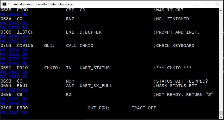
Here is a sample trace matching all signals (every CPU bus cycle). The format is:
<type>,AAAA DD<cr><lf>
Tracing with symbols
With a well-structured trace text records it becomes possible to intercept them, match them up with assembly listing file and display them in rich symbolic format. This is possible by running a simple utility on the host which:
Here is the event handler that fires on every received character from COM port (note that LF (presumed end of trace record) triggers the action:
        static void Port_DataReceived(object sender, System.IO.Ports.SerialDataReceivedEventArgs e)
        {
            string received = comPort.ReadExisting();

            foreach (char c in received)
            {
                if (c == LF)
                {
                    // leave out the previous CR (TODO - check assumption it was a CR...)
                    string traceRecord = sbTraceRecord.ToString(0, sbTraceRecord.Length - 1);
                    string[] traceValuePair = traceRecord.Split(',');
                    string recordType = traceValuePair[0].ToUpperInvariant();
                    switch (recordType)
                    {
                        // see https://github.com/zpekic/sys9080/blob/master/debugtracer.vhd...
Read more »
The history of Tiny Basic programming language goes back to the same era when first home/hobby microcomputers powered by 8-bit microprocessors started to appear.
Due to ROM/RAM size limitations (2kB each) and the CPU used (8080), the choice of Tiny Basic fell on this version:
;*************************************************************
;
;                 TINY BASIC FOR INTEL 8080
;                       VERSION 2.0
;                     BY LI-CHEN WANG
;                  MODIFIED AND TRANSLATED
;                    TO INTEL MNEMONICS
;                     BY ROGER RAUSKOLB
;                      10 OCTOBER,1976
;                        @COPYLEFT
;                   ALL WRONGS RESERVED
;
;*************************************************************
I took the Tiny Basic source code from CPUville site (by Donn Steward which has many other great retro-computing resources there too) and made two modifications:
(1) changed from Intel 8251 UART to Motorola 6850 ACIA (I/O port locations and control / status register bits):
;--- definitions for Intel 8251 UART ------
;UART_DATA    EQU 2H
;UART_CTRL    EQU 3H
;UART_STATUS    EQU 3H
;UART_TX_EMPTY    EQU 1H
;UART_RX_FULL    EQU 2H
;UART_INIT1    EQU 4EH    ;1 STOP, NO PARITY, 8 DATA BITS, 16x CLOCK
;UART_INIT2    EQU 37H    ;EH IR RTS ER SBRK RxE DTR TxE (RTS, ERROR RESET, ENABLE RX, DTR, ENABLE TX)
;--- definitions for Motorola 6850 ACIA ---
UART_DATA    EQU 11H
UART_CTRL    EQU 10H
UART_STATUS    EQU 10H
UART_TX_EMPTY    EQU 2H
UART_RX_FULL    EQU 1H
UART_INIT1    EQU 03H    ; reset
UART_INIT2    EQU 10H    ; 8N1, divide clock by 1
;
(2) fixed the "overflow on change sign" bug
When changing the sign of 16-bit 2's complement integer, there are two cases when the MSB stays the same - from 8000H (-32768) to 8000H (and this is an overflow error) and from 0000H to 0000H (not an error). This second case was not handled in original (and was causing HOW? error message when I first ran the benchmark program).
;
CHGSGN: MOV  A,H                        ;*** CHGSGN ***
        PUSH PSW
        CMA                             ;CHANGE SIGN OF HL
        MOV  H,A
        MOV  A,L
        CMA
        MOV  L,A
        INX  H
        POP  PSW
        XRA  H
        JP   QHOW
        MOV  A,B                        ;AND ALSO FLIP B
        XRI  80H
        MOV  B,A
        RET
;
CHGSGN: MOV  A,H                        ;*** CHGSGN ***
        PUSH PSW
        CMA                             ;CHANGE SIGN OF HL
        MOV  H,A
        MOV  A,L
        CMA
        MOV  L,A
        INX  H
        POP  PSW
        XRA  H
    JM   FLIPB            ;OK, OLD AND NEW SIGNS ARE DIFFERENT
    MOV A,H
    ORA L
        JNZ   QHOW            ;ERROR IF -(-32768)
FLIPB:  MOV  A,B                        ;AND ALSO FLIP B
        XRI  80H
        MOV  B,A
        RET
To assemble into binary I used zmac cross-assembler, with -8 command line flag to use the 8080-style mnemonics (instead of default Z80-style). Note that the VHDL project in ISE 14.7 which produces the .bin file to download to FPGA is using the .hex file output, not the .bin (which would be the case in programming EPROMs for example). This process is described in a separate project log.
Running and benchmarking
To test the Tiny Basic, I used the benchmark test program proposed by June 1980 Interface mag article - a very simple algorithm to find first 1000 prime number. Only two minor modifications were done - as Tiny Basic has no INT() - because doesn't support floating point numbers, and commenting out CHR$(7) (which on many somewhat compatible ANSI platforms would produce a beep "bell")
100 REM    -------------------------------------
101 REM    Simple benchmark - find primes < 1000
103 REM    -------------------------------------
104 REM https://archive.org/details/InterfaceAge198006/page/n131/mode/2up
110 REM    -------------------------------------
130 PRINT "Starting."
140 FOR N = 1 TO 1000
150   FOR K = 2 TO 500
160     LET L = N/K
170     LET M = N-K*L
180     IF L = 0 GOTO 230
190     IF L = 1 GOTO 220
200     IF M > L GOTO 220
210     IF M = L GOTO 240
220   NEXT K
230   PRINT N;
240 NEXT N
250 REM PRINT CHR$(7)
260 PRINT "Finished."
270 STOP
Results running at different CPU clock frequencies:
104 REM https://archive.org/details/InterfaceAge198006/page/n131/mode/2up
105 REM   SW210    CPU (MHz) Result (s)
106 REM   100     01.5625 52m23   3143
107 REM   101     03.1250 26m12   1572
108 REM   110     06.2500 13m06   786
109 REM   111     25.0000 3m17    197
110 REM   -------------------------------------
It can be seen that the execution...
Read more »The main point of this project was to recreate a working CPU by following a technical document from 1978, illustrate micro-programming in a practical way and recreate the ICs (especially Am29XX) from the era in a FPGA.
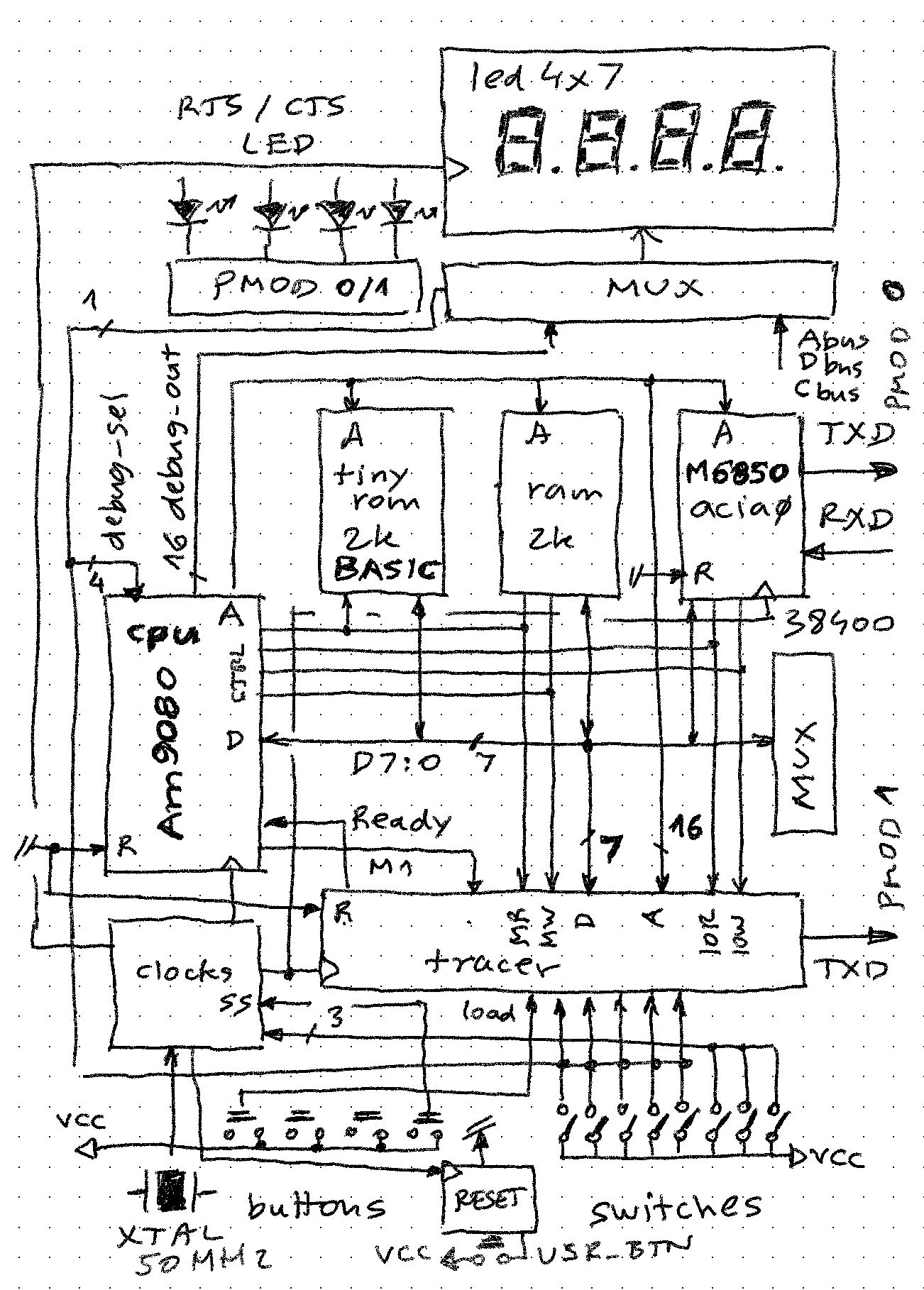
Maybe not the best (which would be to run dedicated test programs) but the most fun way to verify if the CPU works is to create a small working system around it, running Basic.
The small system is similar to SBCs (single board computers) available for many 8-bit CPUs, closest is probably 8085 MiniMax.
Project top level source file (sys9080.vhd) describes the SBC mostly through structural VHDL design approach, and can be roughly represented as:
(note a bug in the sketch: MUX in center right has arrow in wrong direction, it can only drive DBUS, and takes input from either switches or buttons - so CPU can read these as port 00H and 01H)
Key components (as they are named in top-level source file):
cpu
Details are described here. While Intel 8080 compatible, there are some differences:
ram (2k*8)
Source code is here. Very similar to the static RAM ICs of the era, such as 6116. It is implemented using Xilinx-specific component to be able to fit into the design (ISE 14.7 was not able to map/pack the generic VHDL defined design into the modest Spartan XC3S200A FPGA as the design was getting too big. It repeats 31 time in the memory address space (everywhere outside ROM taken space, so 0800H - FFFFH)
tinyrom (2k*8)
Similar to EPROMs of the era, such as 2716. It contains Tiny Basic, or can contain any other 2k system program (e.g. a monitor) in the 0000H-07FFH address space (8080 family of CPUs require readable and defined RST n target addressed in range 0000H-0038H. Its size and contents is defined in parametric way:
-- ROM 2k at 0000H to 07FFH
-- See http://cpuville.com/Code/tiny_basic_instructions.pdf
    tinyrom: entity work.rom1k generic map(
        address_size => 11,
        filename => "..\prog\zout\tinybasic2dms.hex",
        default_value => X"76" -- HLT
    )
    port map(
        D => data_bus,
        A => address_bus(10 downto 0),
        nOE => nTinyRomEnable
    );
This project log provides details how a file name parameter leads to build-time initialization of ROM memory using hex file format.
acia0
This device mimics the popular MC6850 ACIA of the era. Mimics because it only supports features in its control and status registers that are used by Tiny Basic. For example, no interrupts for example or modem control pins are supported. It is an aggregation of:
D <= d_out when (int_read = '1') else "ZZZZZZZZ";
d_out <= rdr when (RS = '1') else status;

status(7) <= '0';        -- no interrupt
status(6) <= err_parity;    -- parity error
status(5) <= err_overrun;    -- receiver overrun
status(4...
Read more »
Context
Given that this CPU implementation is an almost canonical example of microcoded design as envisioned by AMD - and a showcase of their Am29XX and Am25XX ICs - it is very helpful to go over at least chapters I and II of the "Bit-slice microprocessor design" book for better understanding. After that, the application note provides a great explanation of this specific CPU implementation. All source files to implement the CPU are under this folder.
General notes
In this CPU re-creation I attempted to follow the original application note as closely as possible. The description there is very detailed but also sufficiently clear to allow not just the understanding of this implementation, but how it can be adapted to other similar processors. The schema of the CPU is in figures 3-5 in the application note, and the VHDL top-level file is organized to follow those figures, and IC names/id so that the code can easily be mapped to schema and vice versa.
VHDL has the ability to describe circuits in both structural and behavioral ways, and in any source files these can be freely mixed. In this case, top-level is mostly structural (building blocks), for example:
-- data bus register (FLAGS)
-- 7 6 5 4  3 2 1 0 --------
-- S Z 0 AC 0 P 1 C --------
        u102: Am2918 port map (     clk => CLK,
                    nOE => db(3),
                    d(3) => '1',
                    d(2) => '0',
                    d(1) => '0',
                    d(0) => u92_pin7,
                    o(3) => open,
                    o(2) => open,
                    o(1) => open,
                    o(0) => flag_cy,
                    y(3) => DBUS(1),
                    y(2) => DBUS(3),
                    y(1) => DBUS(5),
                    y(0) => DBUS(0)
                );

      u101: Am2918 port map (     clk => CLK,
                    nOE => db(3),
                    d(3) => u91_pin4,
                    d(2) => u91_pin7,
                    d(1) => u91_pin9,
                    d(0) => u91_pin12,
                    o(3) => flag_z,
                    o(2) => flag_p,
                    o(1) => flag_s,
                    o(0) => flag_ac,
                    y(3) => DBUS(6),
                    y(2) => DBUS(2),
                    y(1) => DBUS(7),
                    y(0) => DBUS(4)
                );
While the implementation of individual components in mostly behavioral (description of functionality):
entity Am2918 is
    Port ( clk : in STD_LOGIC;
           nOE : in STD_LOGIC;
           d : in STD_LOGIC_VECTOR (3 downto 0);
           o : buffer STD_LOGIC_VECTOR (3 downto 0);
           y : out STD_LOGIC_VECTOR (3 downto 0));
end Am2918;

architecture Behavioral of Am2918 is

begin

y <= o when (nOE = '0') else "ZZZZ";

load_q: process(clk, d)
begin
    if (rising_edge(clk)) then
        o <= d;
    end if;
end process;

end Behavioral;
Components
The parts list in the original design (59 ICs) closely matches the component list from the FPGA project:
However, there are some differences for sake of simplification:

Thanks a lot! I talk a bit more about microcoding in this project entry, I might expand it there: https://hackaday.io/project/172073-microcoding-for-fpgas
I believe most of AMD microcoding approach and tooling as well as ICs was horizontal at the time. So is my "home-brew" microcode compiler and the VHDL code it spits out. It could be adapted though. Right now it just supports some microinstruction width optimizations such as field overlaps.
3 2909s were in the original article and design so I left it for the sake of staying true to original, but then I slightly "optimized" and rolled them into one virtual IC.
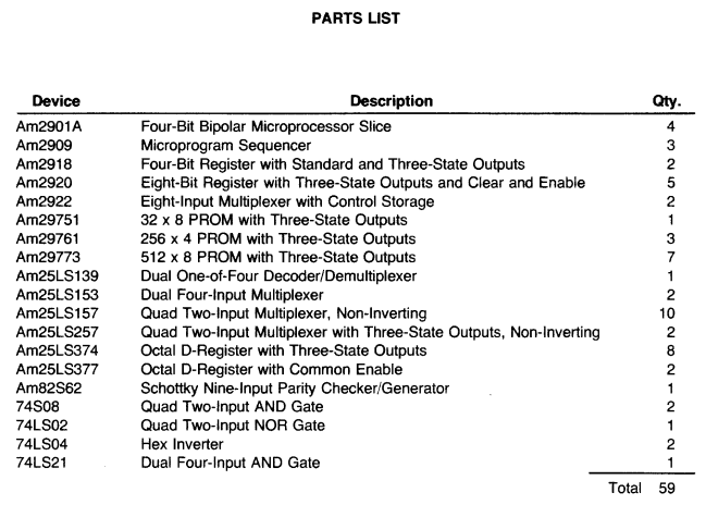
Great Job! Nicely Done! You might mention the difference between Vertical and Horizontal microcode architecture. (This one is horizontal). My only suggestion is to replace the 3 2909's with a single 2910 which would give the micro machine more flexibility.