thpoll
-
Communication
03/28/2023 at 08:22 • 0 comments
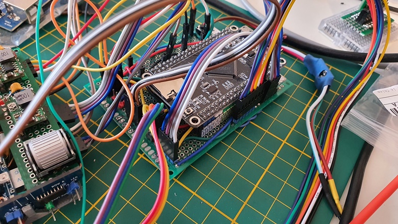
A split keyboard needs two sides.
Before ordering another PCB (for the right side), I want to make sure that the communication works. And luckily you always get two PCBs when ordering an assembled board, so I have two left sides. Enough to test (so stay tuned for another update with some results)!
Why do it like that? It gives me the chance to correct mistakes from the left side (see bodge wires posted earlier) and test an improved right side :)
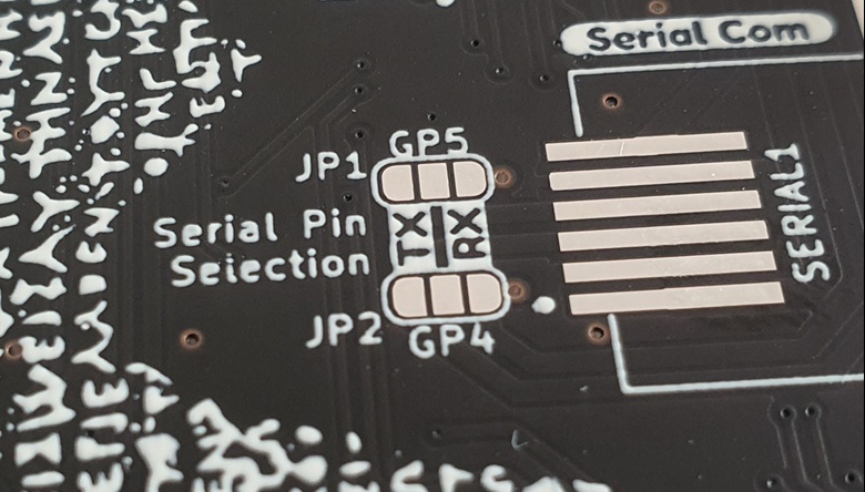
From the beginning I prepared to cross Rx and Tx via solder jumpers so that I can run that test:
![]()
Maybe a bit over-engineered and in the meanwhile I found out that QMK supports half-duplex serial communication via a single wire, but I will give it a try. Unfortunately, I put these solder jumpers on the front side, which is inaccessible if I put the keyboard plate on.
Right next to the solder jumpers you can see the SMD footprint of the RJ12 connector. It is not that common for split keyboards, but I do like the fact that it doesn't expose blank pins like TRRS (which is indeed compact). I've seen a lot of people using USB-C but imho that's also wrong as it's not a standard conforming USB-C. Happy to hear suggestions!
Btw, did you recognize that the picture of this post already shows some 1.25U? I do like them a lot. Let me know your opinion about it~
-
A Focus On Software
03/28/2023 at 08:20 • 0 comments
Let me talk a little bit about software, since this also takes time - apart from my hardware challenges!
Okay, so next to my QMK keyboard firmware, I need some glyph rendering for my OLED screens. To truly support multiple languages, I have handle characters beyond ASCII-7/8.
Initially, I started to use the Adafruit-GFX Library as base, which provides the rendering of basic ASCII characters (a font has to be converted to pixel data from a .tft or .oft file of choice).
To support characters for Japanese, Korean, Arabic, etc. I had to first extend all std::sting / const char* to std::u16string (I know there are 4 byte characters, but for my use cases, 2 bytes are enough for now), which wasn't a big deal.
Next, I needed to extend my own interface of the keyboard firmware to provide other fonts (pixmaps) for the new character ranges. For instance Japanese Hiragana characters are in the range from 12353 to 12447 (instead of the printable ASCII range from `space` 32 to `tilde` 126). To do that, my font rendering accepts an array of fonts and tries to find the matching character in the range of the first provided font and looks up in the next font if that fails.
To prove that this approach works, I started manually patching the generated font files (.h files), but over time it became a burden and so I decided to update the fontconverter as well.
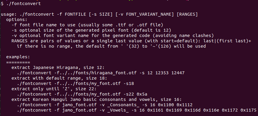
Also here, the first step was to extend indices from 1 byte to 2 bytes and remove checks that narrowed the output to the ASCII range. For more convenience my fontconverter version also allows multiple ranges, eg from 32-126 and from 138-142 at once. However, due to some restrictions in the font rendering library the entries of characters in-between the ranges will be filled up with zeros. So, if the gap between two ranges is big it might be still better to split that up into two separate ranges (a lot of zero also need some space).
You can find that fonconvert version here: https://github.com/thpoll83/Adafruit-GFX-Library
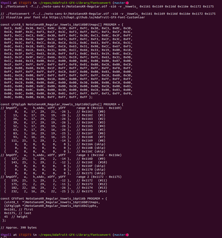
Let me show you a small example to generate all isolated Korean vowels (I'm using Google's Noto Korean font - you can use any font that has Korean vowels), which I can specify with 3 ranges 0x1161 to 0x1169, 0x116d to 0x116e and 0x1172 to 0x1175:
![]()
In the output you can see some zero-ed entries in-between the ranges as described - annotated with 'skip'. You might have noticed the slightly changed parameters, so here is the `usage` output:
![]()
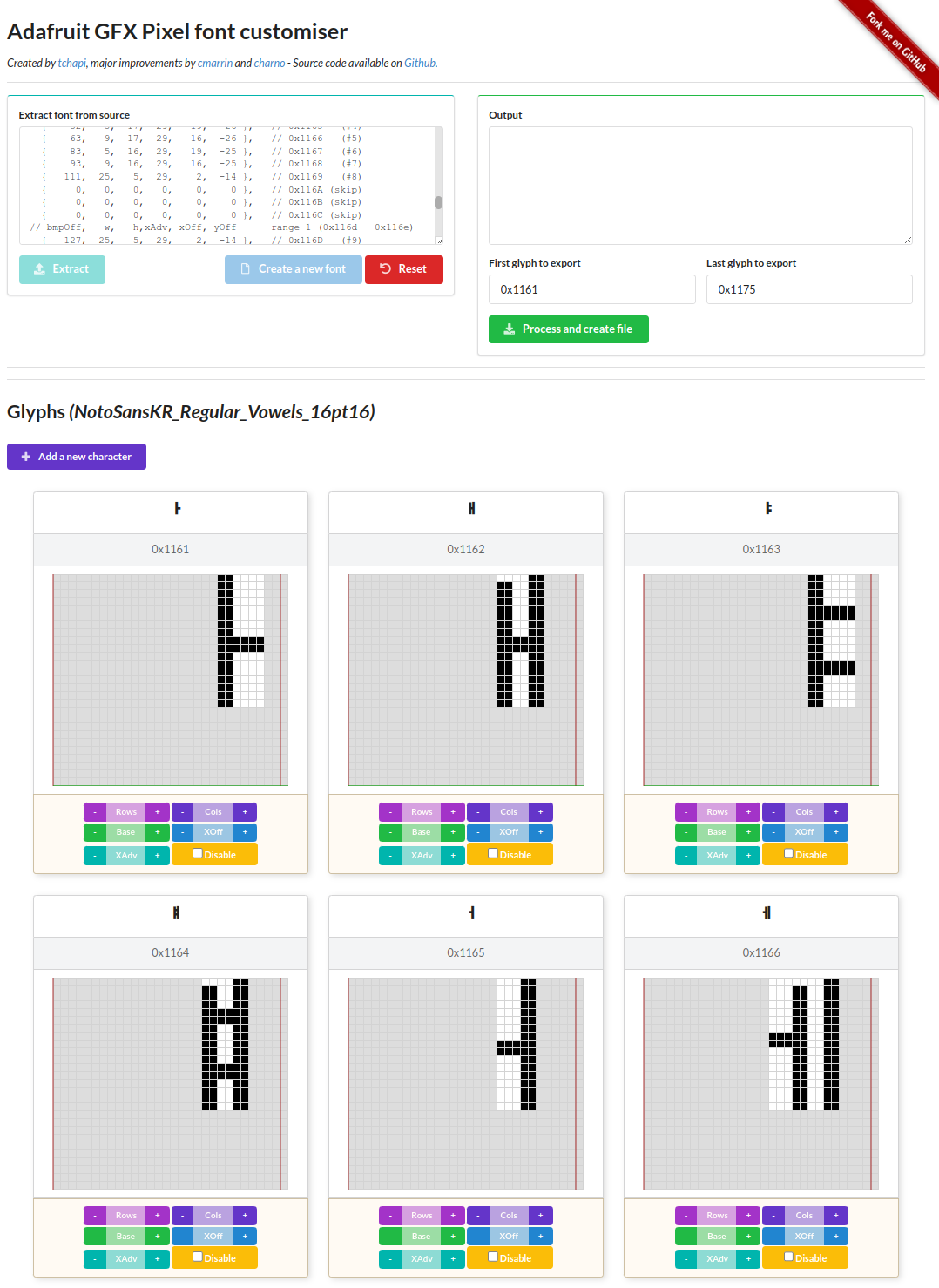
I usually evaluate the result right away with this awesome online tool: https://tchapi.github.io/Adafruit-GFX-Font-Customiser/ You can just copy & paste the output and it will visualize the generated pixel font. In addition allows you to modify the font as well. A really useful tool, which thankfully also works despite my changes to the output format:
![]()
If everything fits, the generated text goes into a .h file, which is than used by my QMK firmware, which you can find here: https://github.com/thpoll83/qmk_firmware
There wasn't much progress on the firmware recently as I was on a holiday break with my family ;) I hope you enjoyed this software post and see you next time!
-
Testing Key Switch Compatibility
03/28/2023 at 08:15 • 0 comments
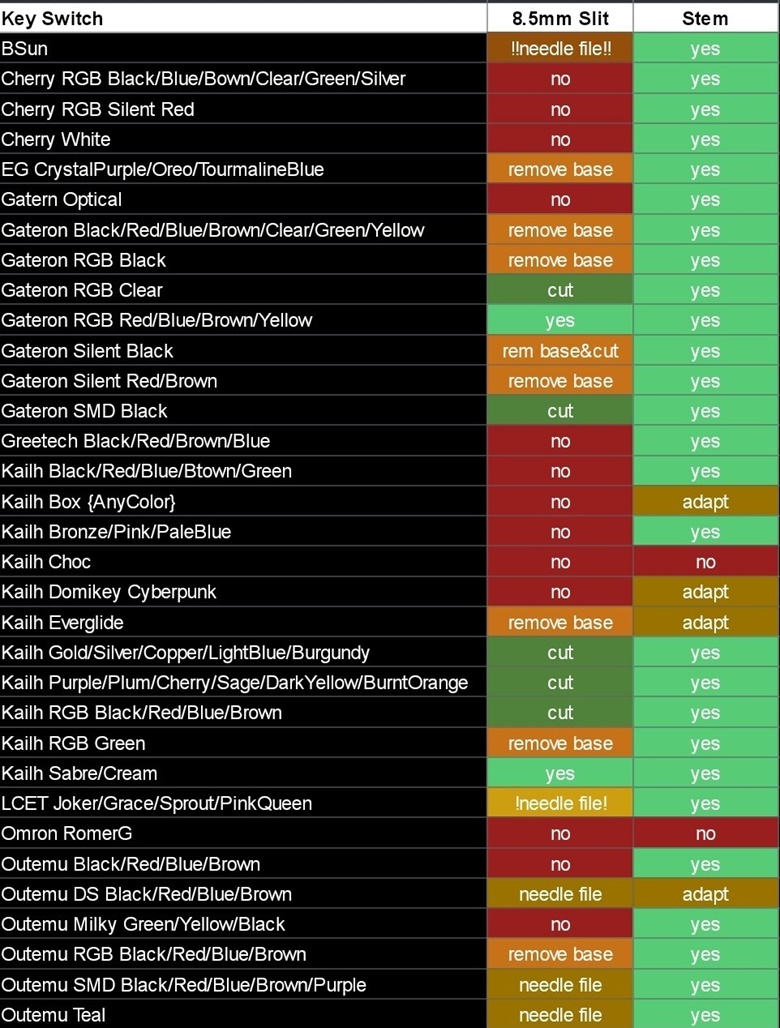
I finally got a set of test key switches to check which are compatible with my PolyKeyboard.
What's needed? Actually only a LED slit that is 8.5mm wide. This is usually not mentioned in any datasheet, so I decided it's best to try out!
The result table:
![]()
From that you can see that only a few Gateron switches and the Kailh Sabre & Cream switches work without modification.
Luckily you get much more choice when you cut away the little centerpiece in the LED slit. This can be done with either a sharp knife or a needle file. With that you can use all switches with a compatible stem (the cross) and all entries that say "needle file" for the 8.5mm slit. I added an exclamation mark in case you also have to trim away a bit plastic from the side (so in fact a bit smaller than 8.5mm).
If you are willing to modify your switches a bit more, you will get a much wider selection. For example, there are a couple of switches that have a slit, but at the bottom (base) there are only 4 holes for the LED pins. With a Dremel or similar you could easliy cut though the base (but it will be a lot of work... for each and every switch).
Of course this list is not complete, not at all. It's only what I was able to test. Let's hope that this list expands at some point!
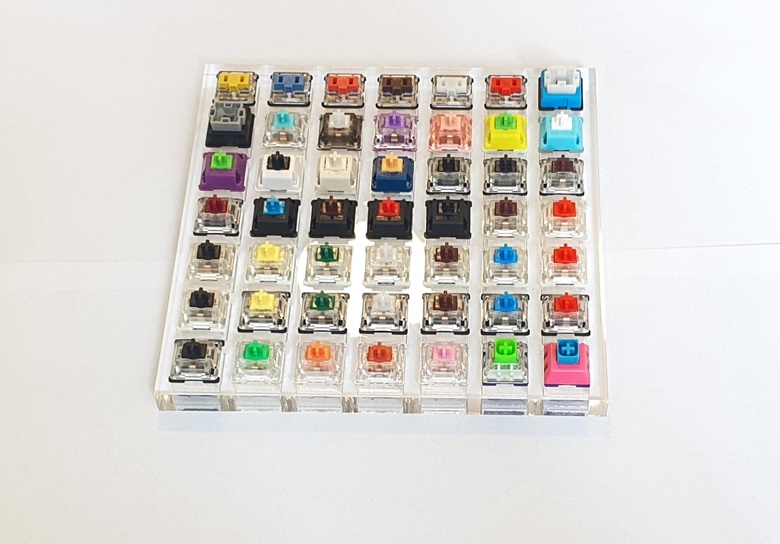
I really like the low profile key switches from the second set of test switches and maybe I can use such switches for the lower 3 thumb switches (or even the whole bottom row?):
![]()
Unfortunately those have an incompatible pin layout, so I'm thinking about getting some Cherry MX low profile switches and just cut a slit into them...
-
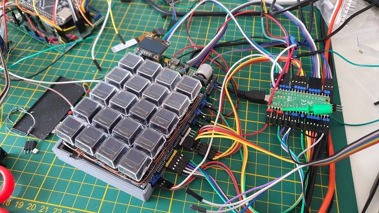
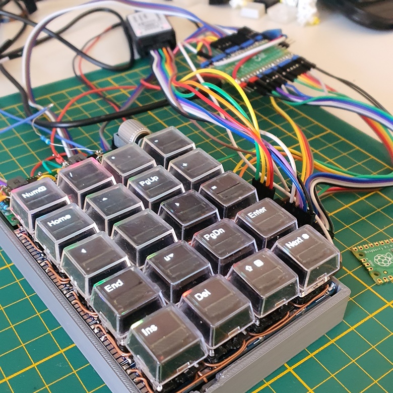
Assembling The Left Side
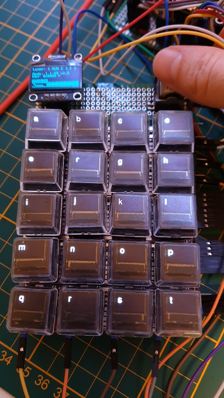
03/28/2023 at 08:12 • 0 comments
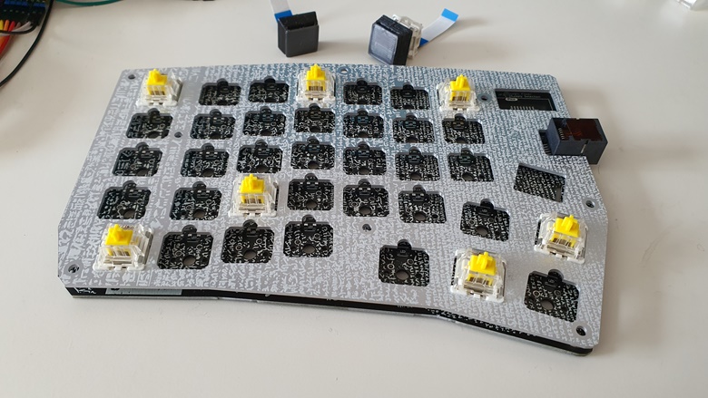
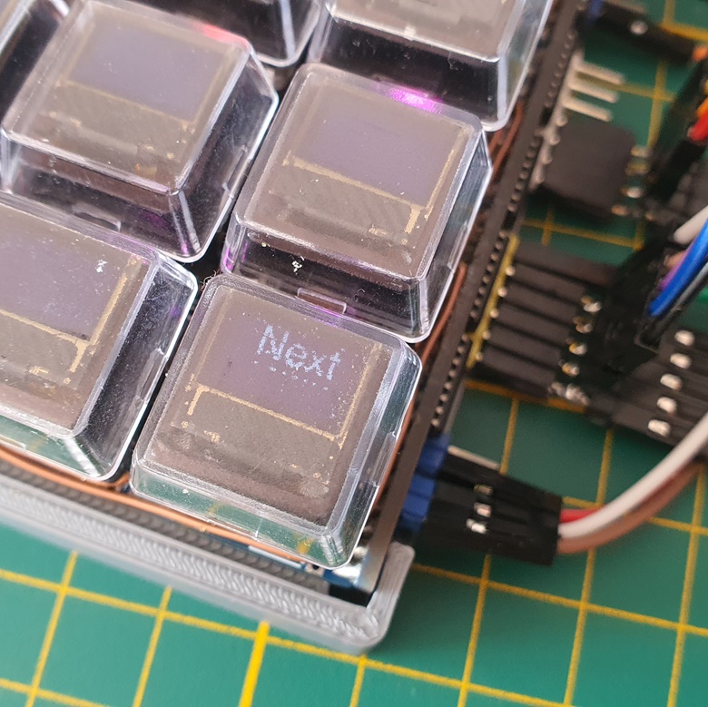
I had to wait a little bit longer to assemble the left side as I was waiting for the Mill-Max 0305 sockets to arrive. Of course, I could just solder the key switches to the PCB, but that would make eventual debugging or applying bodge wires much harder. Better wait a bit!
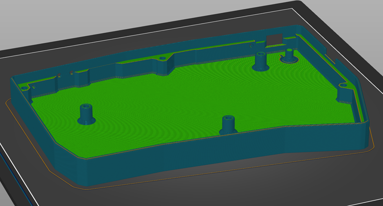
At least I could use the time to prototype a fitting case with the 3D printer:
![]()
I swear, I measured it before printing, but it doesn't always work right away. The current case also provides some hohls to mount tenting stands, but I haven't tried those yet.
![]()
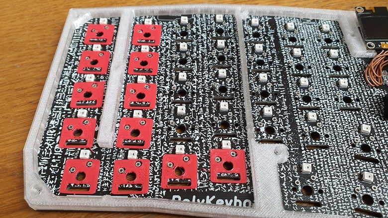
At the time the sockets arrived, I found out that these sockets make the switches stand out a little more than before so I had to print some underpads:
![]()
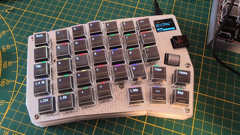
And with that the sandwich got a bit thicker and the displays flex cables got some more clearance, so actually, I could print the case again, reducing the height by 2 more millimeters. But that's for another day! For now I was just happy to finally see the left side come together:
![]()
Here is a very short video I posted on twitter: https://twitter.com/thpoll2/status/1534847633612845058
Right now I'm working on the firmware as there is still plenty of stuff to do to really show what I try to achieve and of course there is also the right side which needs to be revised and assembled, so it will not get boring any time soon.
-
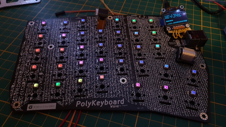
Assembled PCBs and Plate Arrived
03/28/2023 at 08:09 • 0 comments
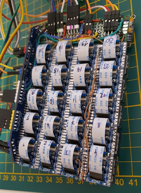
An exciting moment as I worked really long time to get to that point.
My designed keyboard PCB and aluminium plate arrived! As usual for JLCPCB you get a minimum of 5 pieces. If you chose to assemble, you have to assemble at least 2! However, that is fine for me, as it gives my the chance to connect two boards of the split keyboard and prototype a bit further. Sure, two left sides, but it doesn't matter for testing the software communication.
First, I tested if plate and PCB fits together:
![]()
I really like how the silk screen turned out and the alignment of PCB and plate is great. Unfortunately, the key switches sit a bit lose as I needed another notch at the top of every switch to let the LED shine through (the actual LED slit will be occupied by the flex cable of the OLED displays). So, next time, I will try to make them a bit tighter.
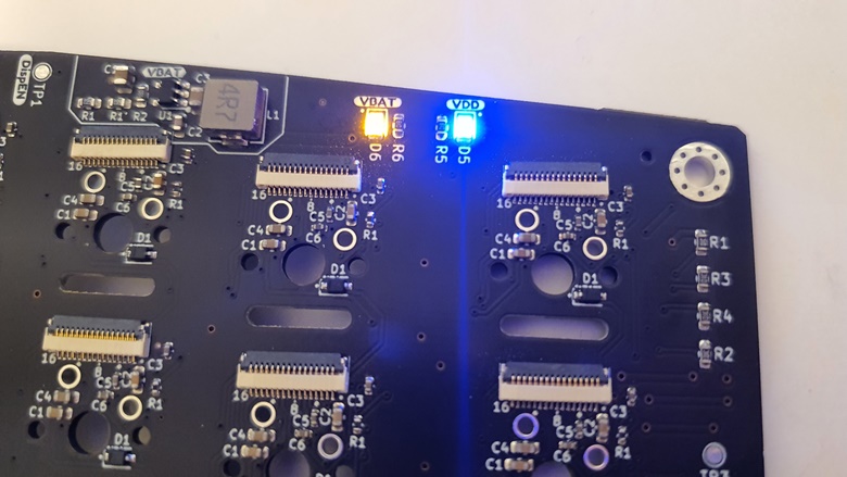
Testing the power supply next:
![]()
Glad that those work and also give the right voltages. I was a bit worried about that as I don't have much experience here. In the end I just followed the data sheet of the ICs and hoped it works out (on my previous macro pad I used boost/buck converters from AliExpress but wasn't too happy with them).
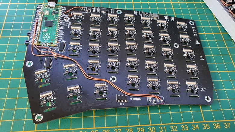
As JLCPCB does only one side PCBA, I had manually solder on the front side LEDs and one of the shift registers, which I decided to put under the keyboard status display. In the end not the best decision since the space under the display is much more limited than expected and I had to move SMT parts on the backside of the display:
![]()
Luckily, that all worked out and a first test shows all LEDs and the status display come to live. This was still without the RP Pico directly soldered to the backside.
Before doing that, I had to apply some fixes:
![]()
Not too bad, but definitely have to fix that for the right side. I somehow managed to exchange the SPI clock and data line and also one pin needs to stay unconnected as SPI requires to setup a MISO pin despite the fact that I have no device talking back to the MCU. With that, some pins shifted around and caused some additional bodge wires as well.
Nevertheless, with these modifications, the board was ready to drive the small displays:
![]()
-
Designing A Keyboard PCB
03/28/2023 at 06:45 • 0 comments
At the beginning of my keyboard journey I was sure to make a standard 100% layout, now, as I got more into that topic, I figured out that I don't want that any more and maybe people who are more into mechanical keyboard can understand.
So ultimately, I decided to go for a split keyboard with 36 keys plus one encoder on one side. That is about the maximum I can operate with a RP2040 without the need of a port extender.
As I already made my first steps in KiCad with the PolyKB Atom, I felt confident enough that this works out.
Maybe I should have done some more studies on ergonomics, but we all have to start somewhere, so this how the left side of my keyboard will look like:
![]()
As you might be able to see, the RP Pico board can be soldered to the PCB on the backside (unfortunately it only has a Micro USB as we know :/ ) and I decided to use an RJ12 jack to connect the two boards.
I know a TRRS jack would be sufficient, but it feels a bit... "strange" to power the second board with that, as the power "pins" would be totally unprotected when disconnecting in operation. Also, I was not sure if I need another pin for bi-directional communication (maybe not, but we will see)
For the keyboard plate I'm using aluminium as I can order it together with the PCB from JLCPCB (as they are making aluminium PCBs as well) and I can design it in KiCad as well, no need for anything else.
Since it is possible to add a silk screen to the aluminium plate I wanted to have an appropriate design for my project: True to my goal to make a keyboard that speaks multiple languages I found the perfect fit, the oldest piece of multilingual history - the Rosetta Stone.
![]()
As I wanted to have the shiny side on top, I designed the plate with the silk screen directly on the front aluminium and the solder mask on the back (where you could apply another silk screen).
JLCPCB doesn't make guarantees about the quality of the silk screen on that side but I will find out :)
-
Moving to the RP2040 as MCU
03/28/2023 at 06:43 • 0 comments
Chip shortage. Any more explanation needed? When I started, the STM32F407 was cheap, fast and had plenty of IO pins and therefore, an ideal choice I thought :)
Now you have to pay 40 bucks for the dev board I used and as I'm trying to make a dev kit out of this project I need some more accessible components.
The RP Pico (with an RP2040) comes at a price of 4 Euro, so I ordered a few boards to get started.
Next, I removed my old mainboard:
![]()
Goodbye and thank you for your service!
Here comes the new generation (and there are significantly less IO pins, actually, I need them all and some more):
![]()
Right, so I had to hard-wire the enable pin of the displays power supply to +3V3, there was just no pin left.
And it took some time with the logic analyzer to figure out the little differences in the SPI setup to finally get something showing up:
![]()
Exactly one key gave me something and that something was also distorted. But after getting the timing, reset, d/c etc. signals and default low/hight states right, ALL displays were willing to work!
![]()
Another step forward and in parallel I started with my efforts in designing a more complete keyboard PCB.... still based on my Atoms.
-
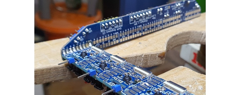
Combining all PCBs to a Macro Pad
03/28/2023 at 06:42 • 0 comments
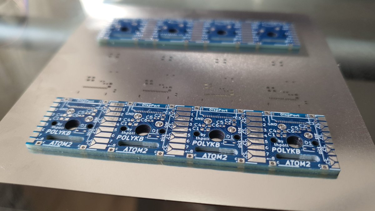
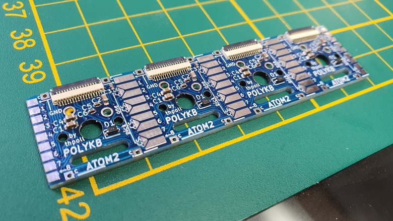
My next goal was to get a full macro pad working and since JLCPCB sends you always 5 PCBs as a minimum, there were still a few more rows with 4x1 Atoms left.
The assembly was labor intensive as I had to bake all PCBs first, solder them to the side connector and apply the fixes with some bodge wires:
![]()
Next, I extended my QMK firmware and got all diplays working (after some debugging) - Halleluja!
![]()
There were still some minor issues, not all displays worked trouble-free, extending the FFC is not easy :(
Even though my intention with the Atom's side-connectors was to make it easily buildable and affordable for everyone, it turned out quite some work. Maybe a ready made PCB would be worth a try...
Also my used MCU, the STM32F407 became unavailable, which made me think about alternatives.
Luckily the state of the RP2040 QMK branch looked already promising so that I decided to convert the macro pad to the RP Pico!
-
4x2 Proof of Concept
03/28/2023 at 06:40 • 0 comments
Here is the first prototype that I consider as base going forward for a bigger test setup.
That's how the PCB arrived:
![]()
And I'm very happy how they turned out (baked in an old toaster):
![]()
For the prototype: All 8 displays can be updated individually, and purely to test the system the first 4 displays (from the bottom!) and their CS lines are controlled by the first shift register (even though it could handle 8) and the second row is controlled by another shift register daisy-chained to the first.
This setup already runs QMK, you can find the firmware on my git repo: https://github.com/thpoll83/qmk_firmware/tree/PolyKeyboard/keyboards/handwired/polykb
It's not actively maintained as I moved on to another keyboard layout (and MCU) but I wanted to keep it for reference.
Thanks to QMK it already perfectly works as keyboard and I can use it's integrated layer system I can update the keys whenever a layer switch occurs.
I purchased a cheap logic analyzer to investigate all SPI and shift register signals as troubleshooting only on the software side is close to impossible (at least for me).
Here a video of the working version:
-
Atom Pinout Details and the Connector
03/28/2023 at 06:38 • 0 comments
Again the pin-out for reference ;)
Let's take a look at the keyboard matrix pins `c`, `r`
The `c` is used to connect all `Atoms` ortholinear or shifted by 0.25U/0.5U (compared to the next row). This pin is present two times, on the left and right and also on the front- and backside.
For the `c` pin the wiring to the next row depends on the matrix setup.
The `r` / `Row` pin should be always aligned with the next PCB and is only present on the front side.
Power Supply`+` / `VLED`
Voltage supply for the LEDs, which you should connect to a 3.8V regulator with enough Amps to drive all LEDs. `3V3` / `VCC`: Voltage supply for the display logic. `V🔋` / `VBAT`: Power supply for the OLED display's charge pump and should be between 3.5V and 4.2V (I run it at the recommended 3.8V).
`⏚` / `GND` Pin
The common ground.
LED Data Pins`o`, `i`
The only important thing to watch out is that the `o` / `LED Out` pin of a LED in use is connected to the next `i` / `LED In` pin in use. Keep that in mind when skipping some LEDs in the middle. Otherwise you can just connect every `o` pin with the following `i` pin.
SPI Pins`Rs`, `SI`, `DC` and `Clk`
These are all SPI pins used to control the OLED display. Just connect them to the `PolyKB Connector` - more detail follow below. Sorry for the short names on the PCB, but there wasn't any space to write them full length.
Chip Select Pins `1` ~ `8`
Up to 8 `PolyKB Atoms` can be connected in a row and each `Atom` needs one assigned `CS` pin. You simply do that by making a solder bridge between the number of choice and the triangular `CS` pin on the backside.
Example for connecting the `Atom` on the left with `CS` line `3`:
![]()
In a full row you would connect the first `CS` to `1`, the second `CS` to `2`, all the way up to the last with `CS` and `8`.
Connector
Any `Atom` can be directly soldered to the next `Atom` without any wire. That also works for the `Connector` which can be solder to the first `Atom` in a 90 deg angle:
![]()
The `Connector` contains the shift registers used to pick the right `CS` line to control the displays individually.
Right now there is a `Connector-R` and a `Connector-L` so that we can make a row of up to 16 `Atoms` without any gap. The first 8 `Atoms` are controlled by the `Connector-L` (of course on the left side) and the next 8 `Atoms` by the `Connector-R` (you already know it - on the right side).
The only important part is that the 8 `CS` lines (all of them) should NOT be soldered together in the middle, you should even better file/rasp of the edge in the middle to make sure there is no electric connection. The rest of the pins can be connected. Multiple `Connectors` also need to be chained so that the `Shift Out` pin from the previous `Connector` is wired with the `Data In` pin of the next one.
That's the theory, next time I will post some more facts on the hardware assembly.