NNNI
NNNI-
Don't Shoot the Messenger!
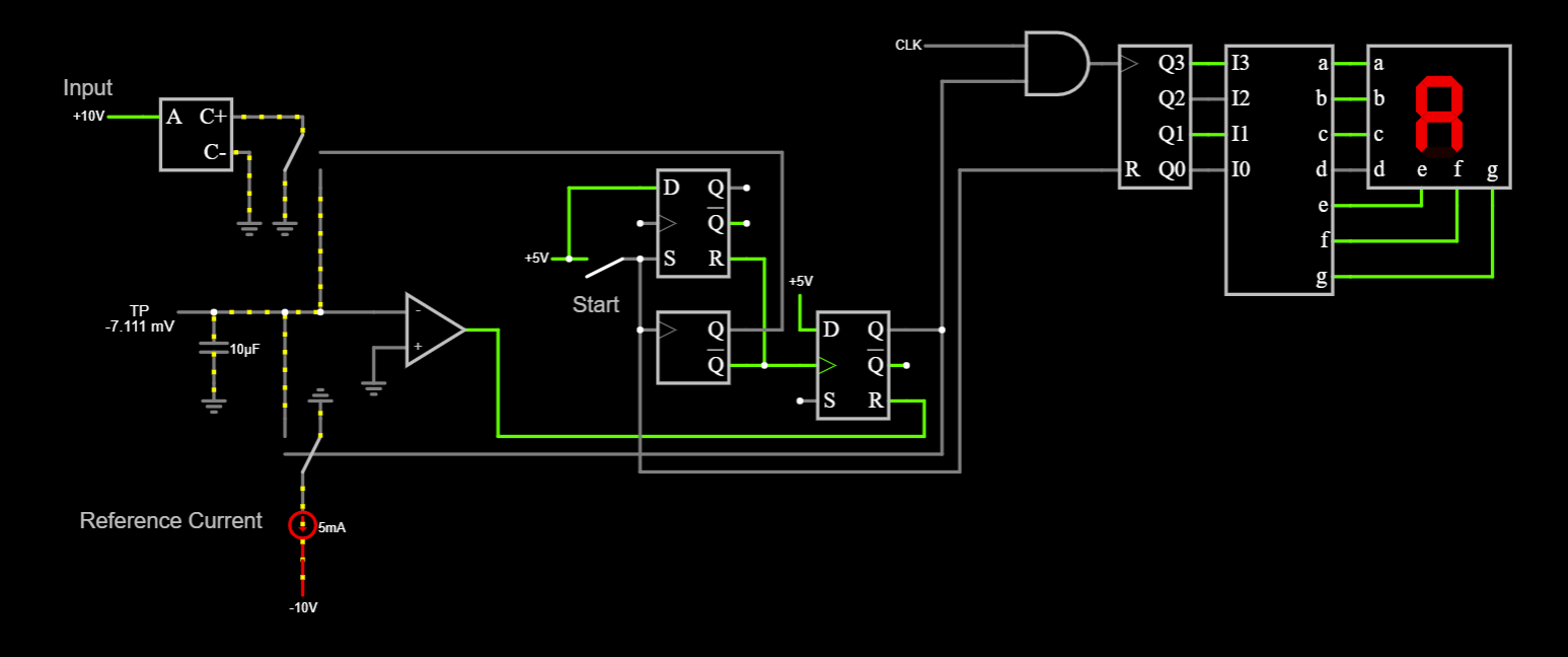
06/15/2023 at 19:07 • 0 commentsAfter the successful experiments described in this log, I assumed that my troubles with the ADC were finally over and I was looking forward to seeing some useful readings.
![]()
After I replaced the troublesome and hard-to-find machine pin headers with regular pin headers, the board was ready for its first full power-up in almost 10 months.
![]()
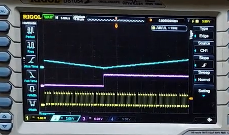
I was glad to see that everything worked just fine. The sample rate of my scope leave something to be desired.
I set up the code to send a stream of data to my computer through USB serial, logged the charge balancing counts and residue counts before and after, and plotted the residue reading difference in Excel.
![]()
Almost as if I had made no changes to the board, the severe noise and banding was back, and I had no clue what was going on this time.
![]()
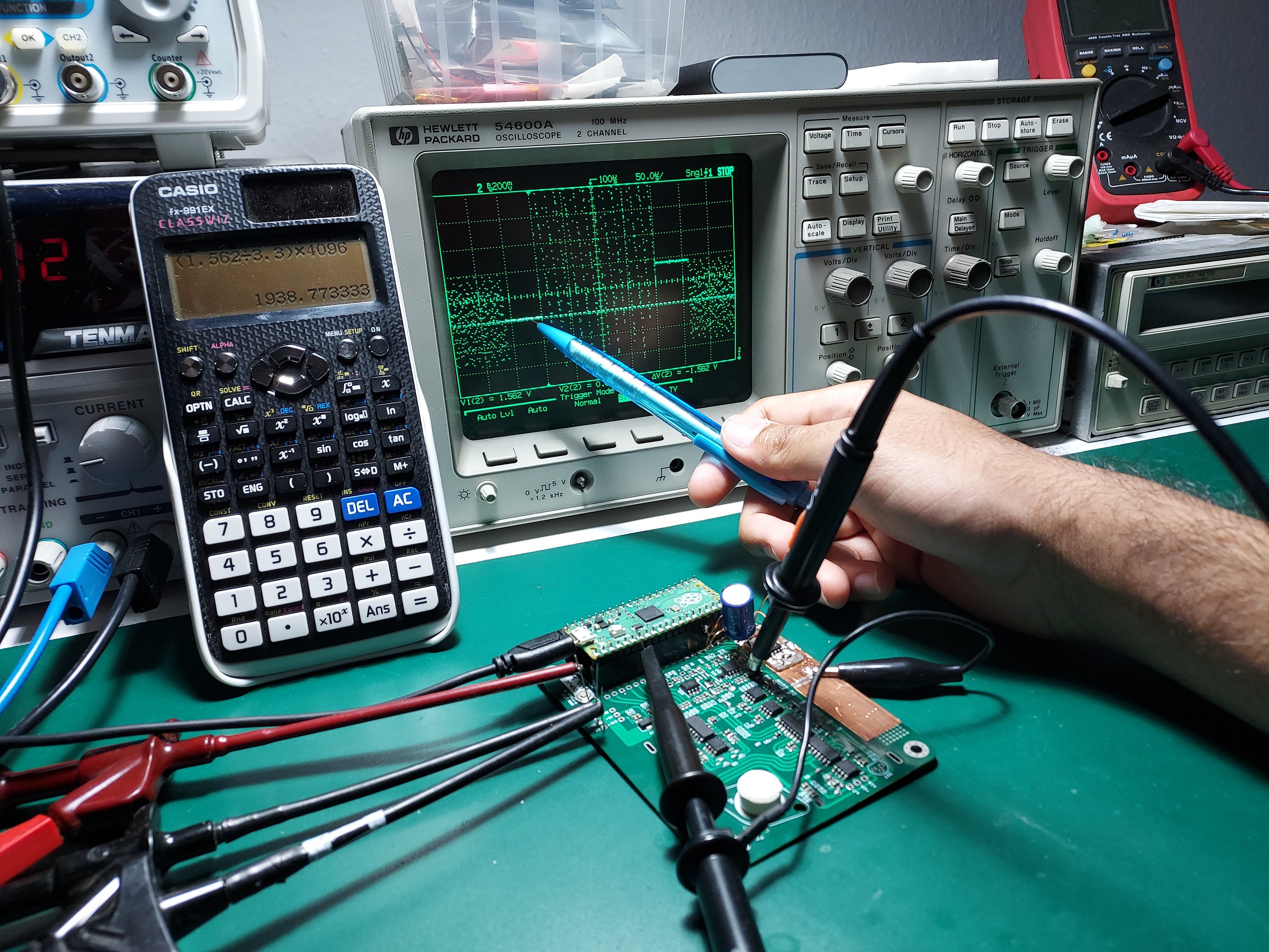
I brought out the calculator and elbow grease and manually checked the voltages on the input of the residue ADC, and made some interesting findings.
The first flat area, which is where the residue ADC makes a measurement of the integrator state before charge balancing, corresponded perfectly with the second residue variable, which is supposed to be the integrator voltage after charge balancing. The pre charge balancing value didn't correspond with the voltage at the ADC input at all.
This got me thinking. I realized that there was a dummy measurement made as soon as the Pi Pico was powered up, in order to put the state machine in dithering mode. During this time, the residue readings were not read and could possibly be clogging up DMA.
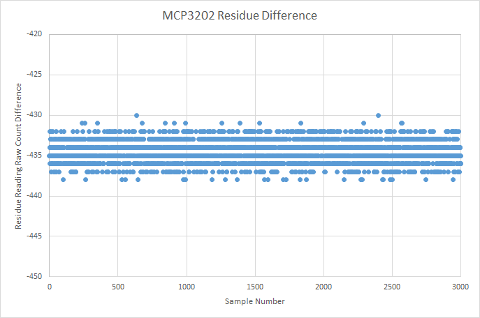
Since I knew the second value being returned was correct, I kept that as such, and moved the first value up by one column in Excel and then plotted the difference.
![]()
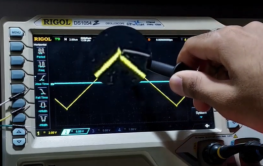
To my surprise, the difference now corresponded perfectly with what was expected. Something was causing the first value being returned to be delayed by one reading. I made a crude diagram to show what was going on.
![]()
One of my initial suspects was a software bug somewhere in the residue reading process, but it was not where I expected it to be!
-
Integrators, DAM Switches and Speed
05/15/2023 at 22:17 • 0 commentsAnother line from The Art of Electronics (3rd Edition) caught my eyes.
More specifically, it’s easy to show that the ΔV term by itself yields the correct input voltage for a measurement whose duration equals a single clock cycle (i.e., Tmeas = 1/ fclk).
Basically, if the integrator is allowed to charge up for a certain time period and the residue ADC reads the integrator voltage before and after measurement, you can get the original input voltage back using the formula:
Here, Vin is the input voltage to the integrator, R and C are the integrator resistor and capacitor values, dV is the resolution of the residue ADC and dt is the integration time.
If we can vary the integrating time correctly, we can measure full scale voltages like 10V with a short integration time (to prevent the integrator from saturating), and small voltages like 1uV by integrating for a longer time. Of course, you can't measure large voltages with a high resolution, so this is a floating-point conversion with a fixed resolution, which in this case is the resolution of the residue ADC. At each point in time, there is a specific input to output "gain", which increases with integration time and therefore "programmable". Of course, this requires knowledge of the input voltage to set the "gain" correctly.
Wouldn't it be nice to have a way to keep the integrator roughly zero to get a coarse reading, and using the residue ADC to do a fine reading? Oh wait...
That brings us straight back to the multislope! The charge balancing keeps the integrator voltage roughly around zero while providing a count of the charge needed to do so, and the residue ADC reads integrator state before and after charge balancing to provide finer details.
Now this is not new information, since previous logs already went into depth about how the multislope topology works. I just found this new way of thinking quite interesting.
Let's consider some numbers. The integrator on the current multislope has a 10K resistor and a 1nF capacitor. The MCP3202 residue ADC has a 12-bit resolution, and with a reference voltage of 3.3V can resolve voltages of 1mV. Assuming a measurement cycle is 20ms (1 PLC), the residue reading has a resolution of 500nV according to the above formula. If the integration time is increased to 200ms (10 PLC), the resolution is improved to 50nV. If the integrating capacitor is reduced to 100pF, the same 500nV resolution can be achieved in 2ms.
The takeaway is that with faster integration, that is, smaller integrating capacitor, measurements can be sped up with fast charge balancing.
Out of curiosity, I tried using the formula to crunch the numbers for the 34410A, which boasts 4.5 digit resolution in 20us. It's ADC has a 50K input resistor and a 47pF integrating capacitor and a 10-bit ADC referenced to 1V, so a 1mV residue resolution. For an integrating time of 20us, the resolution comes out to 100uV. in the 10V range, that gives a usable reading of 10.000V, which is 4.5 digits.
There are practical limitations to how fast currents can be switched, and the analog switches used to do the current steering are the limiting factor. The 74HC4053D used in the 34401A meter specifies a worst case switching time of 200ns, which is no good for speed. The 34410A solves this problem using an interesting circuit called a DAM switch, described in US patent 20050024119A1. I assume this circuit was used to overcome the limitations of regular analog switches and could handle the fast switching speeds.
-
Did You Hear That Whistling Sound, Too?
05/06/2023 at 00:18 • 0 commentsIn my case, it was sadly not outer-space type music (Whoooooo!), but the slope scaler amplifier ringing.
![]()
The slope scaler amplifier scales the +/-5V integrator swing to a reasonable 0V to 3V that the residue ADC can digitize. However, even early on, I noticed that the scaler amp had a slight ring to it. I naively dismissed this, since "it's meant to be a DC amplifier anyway". This is potentially a problem, since the output could ring with a sudden load change, like when the residue ADC is sampling.
The simple fix would be to just add a capacitor across R47 and call it done. The value of said capacitor is key - too little won't fix the problem, and too much would just slow the op-amp down unnecessarily. The key is to find the right value.
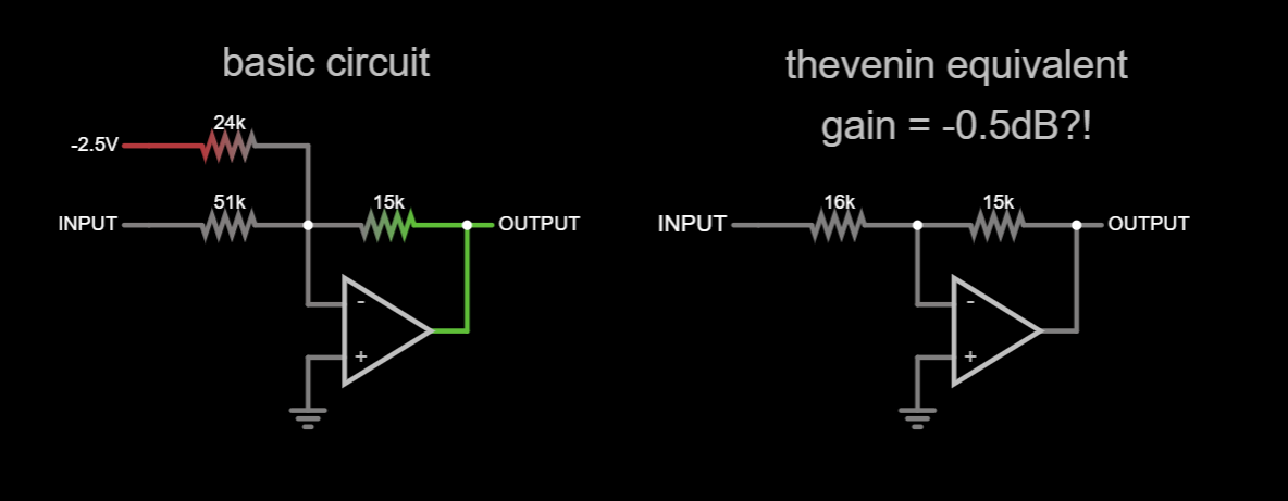
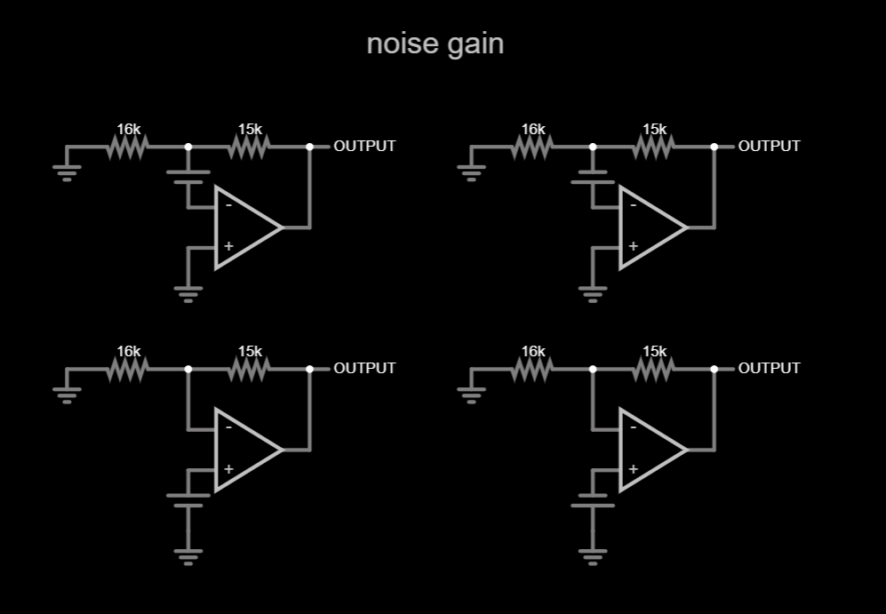
Instead of my preferred method of trying different capacitor values, I tried to take a more analytical approach. The first step in doing that would be to determine the gain of the scaler amp. This sounds like an easy task, since it is basically an inverting configuration. The problem starts when you realize that the gain is less than one, since R47 is 15K and R44 and R45 in parallel (since they both return to a low impedance node) come out to 16K. How does a circuit with a gain of less than one oscillate?!
![]()
The trick (kindly provided by a friend) here is to use something called the noise gain, which emulates input noise by connecting a voltage source in series with the op-amp's input terminals, changing it and seeing how the output changes. The output change for a given input change is the noise gain. This works regardless of the test source polarity or which input it is connected to.
![]()
All of the above circuits are basically the classic non-inverting configuration with a gain of:
Thanks to the 1 term, the gain is always above (or at least equal to) 1, which makes a lot more sense from the ringing point of view. The noise gain is now 5.7dB. I employed LTspice to handle the mathematical heavy lifting from this point on.
I was able to find a model for the OPA197 (and verify it by doing a simple frequency response plot and seeing if it corresponded with the one in the datasheet) and simulate the above circuit.
![]()
The peaking in the frequency response before the gain rolls of below zero is a classic indicator for ringing.
I simulated the entire circuit, and to get the same ringing as I did in real life I had to add 25pF of capacitance to the summing junction node.
![]()
Now to the actual task of compensating it. I'm too embarrassed to reveal my own formula for a rough estimate, but it delivered 24pF, which was a little too much. 10pF worked perfectly.
![]()
After soldering a 10pF capacitor across R47, the results looked like this.
![]()
I found it highly amusing to see that theory and practice corresponded so perfectly for once.
Regarding the 25pF at the summing junction - the value seems suspiciously high to me. I can only assume that the same poor layout that messed with the residue ADC either created some extra capacitance at the summing junction or some stray inductance. Regardless, the ringing is now gone.
Apollo 10's space music turned out to be interference, by the way.
-
A Path Forward
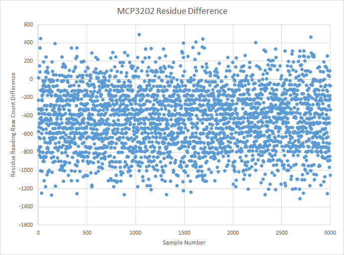
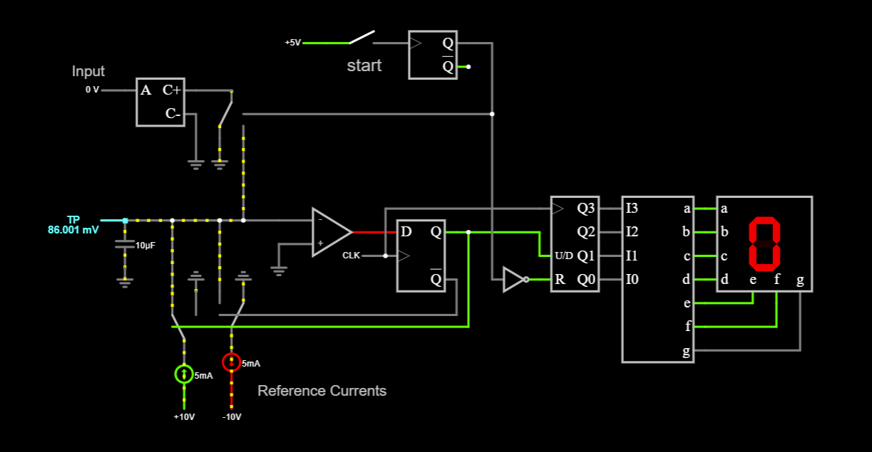
04/30/2023 at 21:51 • 0 commentsMost of the work on Multislope 3I concluded by late July 2022. I was on an informal deadline since I was due to move to Germany on the 15th of August that year to start my higher education. Although readings with a theoretical resolution of 10uV had been achieved, there were still a lot of unanswered questions, the biggest one being the source of severe noise and banding in the residue ADC readings. The residue ADC of choice was the MCP3202, which is a pretty interesting part.
The below chart plots the residue readings (difference in integrator voltage before and after conversion) obtained. The +/-1000 count noise is highly unusual, and upon closer inspection, some banding is also visible.
![]()
Two of the biggest suspects were a bug in the software and PCB layout. To test the former, I desoldered the MCP3202 and put it on a Manhattan prototyping board to ensure neutral layout.
![]()
The MCP3202 IC has a somewhat complicated SPI transaction that had to be split into three transfers of a byte each. Recombining these bytes incorrectly could have possibly led to noise and banding. The input to the ADC was a simple 1K/1K divider connected between VCC and ground. With a neutral layout, I tested four apporaches:
- PIO: I used the RP2040's PIO to set up a custom SPI interface, which let me get the data in a single 18-clock transaction.
![]()
- Original SPI code: I separated and re-compiled the code used in the original project and used it to get a conversion in three bytes.
![]()
- "Direct" SPI: The C/C++ SDK comes with a built-in function to read more than 8 bits "directly", although upon probing it does split the transaction into bytes.
![]()
- PIO with SPI pins: I had to change the wiring a little bit between PIO and SPI readings since the SPI pinout was slightly different. To make sure that the wiring changes didn't affect the readings, I set up PIO to operate from the SPI pins.
![]()
In all four cases, noise was quite acceptable and the readings showed no banding. The MCP3202's input was probed during sampling and the input spike settled within 1/10 of the SPI clock.
The above tests prove that a software bug could be ruled out, since all four approaches have very similar results, with non-PIO readings being slightly noisier.
Once again, I put the MCP3202 back on the original PCB and bodged some connections to the external Pi Pico.
![]()
![]()
The readings were now much worse, with banding being visible in histograms of a single run. This proves with reasonable certainty that the original layout was not optimal.
![]()
This was a four layer board, and the ground plane was on the bottom-most layer, two layers below the MCP3202. Signal and power traces were also routed freely below the part, which was clearly a mistake.
There were still a few more things I wanted to try. The first was a simple filter on the input, consisting of a 56 Ohm resistor and a 1nF capacitor (values copied from Jaromir's NVM). I also added an extra 470uF capacitor across the supply pin and ground.
![]()
The readings are now perfect - not a single bit of noise over three runs of 1000 samples! Looks like the previous poor results were caused by lack of proper layout and decoupling, which is on me.
The above test was performed on a slightly modified setup where I used some copper tape and an SMD adapter on the PCB itself, ready for future testing.
![]()
-
Code overview
04/22/2023 at 13:36 • 0 commentsThe RP2040 was chosen because of its ability to implement custom peripherals using PIO. As explained earlier the multislope topology requires a balancing act of the input in order to not saturate it as well as maintaining a constant number of switch transitions per reading in order to have a known amount of charge injected into the integrating capacitor, to calibrate it out later. This can be done using PWM, where the output of the comparator is used to change the duty cycle of the subsequent PWM cycle. The described can be implemented with bit banging on almost any microcontroller with some software know-how. But hanging up the CPU on several second long measurements is sub-optimal, so implementing it in PIO was more desirable with the added benefit of certainty in the timings and state transitions (since any jitter on the control signals can add up to big uncertainties in the measurements).
The entire multislope algorithm, as well as its idle state (dithering) was fit into a single PIO state machine, almost filling up the available instruction storage, with 30 out of the available 32 instructions being used. Now, let’s take a look at how it was implemented. (It is assumed that the reader has some familiarity with the RP2040 PIO instruction set and architecture)
.program ms
.side_set 1
; 1 side set bit for the MEAS pin

; don't forget to enable auto push
start:
set pins 0 side 0
mov X, !NULL side 0 ; set X to 0xFFFFFFFF
out Y, 32 side 0 ; read the number desired counts
irq wait 0 side 0 ; first residue reading
out NULL, 32 side 0 ; stall until DMA finished reading the ADC
jmp begining side 0 ; got to PWM

finish:
set pins 0 side 0 ; turn switches off
in X, 32 side 0 ; push PWM to FIFO
irq wait 1 side 0 ; second residue reading
out NULL, 32 side 0 ; stall until DMA finished reading the ADC
dither:
dithHigh:
jmp !OSRE start side 0 ; jump out of desaturation when the OSR has data
set pins 1 side 0 [1] ; set pin polarity
jmp pin dithHigh side 0 ; check if the integrator is still high
dithLow:
jmp !OSRE start side 0 ; jump out of desaturation when the OSR has data
set pins 2 side 0 ; set pin polarity
jmp pin dithHigh side 0 ; check if the integrator is high
jmp dithLow side 0 ; stay low

.wrap_target
beginning:
set pins 1 side 1 ; set PWMA high, and PWMB low [01 clock cycles]
jmp pin PWMhigh side 1 ; read comparator input, jump to pwm high state [01 clock cycles]
set pins 2 side 1 ; turn off PWMA if the pin is low [01 clock cycles]
jmp X-- PWMlow side 1 ; else jump to PWM low state [01 clock cycles] (if pin is low we decrement X)
PWMhigh:
set pins 1 side 1 [15] ; keep PWMA high [02 clock cycles] + [28 clock cycles] = 30
nop side 1 [11]
set pins 2 side 1 ; set PWMA low, at the same time PWMB high [01 clock cycles]
jmp Y-- beginning side 1 ; go to the beginning if y is not zero yet [01 clock cycles] = total 32
jmp finish side 0 ; go to rundown when y is zero we don't care at this point anymore
PWMlow:
set pins 2 side 1 [15] ; set PWMA low [4 clock cycles] + [27 clock cycles] = 31
nop side 1 [10]
jmp Y-- beginning side 1 ; go to the beginning if y is not zero yet [01 clock cycles] = total 32
jmp finish side 0
.wrap
When starting up PIO will start from the first instruction in the program, so it begins execution in `start`. Here we first set all the pins into a known state (all off).
Next, using a trick with the binary operations PIO supports, we invert a NULL and store the result in the 32-bit X register. This fills up X with 1s. This is required in order to create a counter inside PIO, since we don’t have an i++ instruction, we need to get creative. By using the jump instruction with the x-- operator we can achieve the same thing just inverted. When the result of X will be shifted to the CPU, it will just perform an inversion on its end to get the count.
The Y register is used to store the requested number of counts to perform, that is just read from the OSR (Output Shift Register, from the perspective of the CPU). In order to not waste instructions on pulling from the FIFO into the OSR auto pull is used. In this context, counts refers to the number of PWM cycles we want to output, the more the better because we have more time over which we accumulate the results. This works only up to a certain point, after which the returns in resolution are diminishing thanks to 1/f noise and dielectric absorption
Next we trigger a residue reading using an interrupt and wait until we get a signal back indicating that it has completed (waiting until some dummy data is put into FIFO, realistically this can be omitted and we can just clear the interrupt after we are done reading the ADC, since interrupts can stall the state machine), setting all the pins to 0 earlier turned off all the switches injecting current, thus leaving the capacitor voltage unchanged (at least on the short timescales of a single ADC conversion cycle). On the CPU side the interrupt starts a DMA operation to read the SPI residue ADC. The reason DMA was used was because the bulk SPI write in the SDK wasn’t working for me at the time for some reason and it was decided to just use DMA instead of spending time debugging the issue.
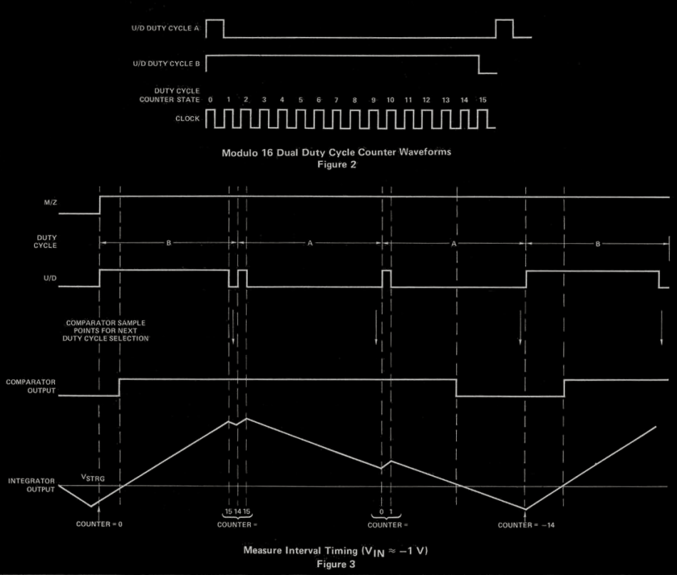
The PWM algorithm was described more in a recent log but the basic idea is that we are using a constant number of switch transitions for the same number of requested counts. This approach is used to address the issue of charge injection from analog switches. Instead of keeping the switch on continuously, it is turned off periodically at constant intervals to avoid accumulating too much charge on the integrator. Essentially what the drive waveform starts to look like is just PWM with two duty cycle levels (in our case it was 1/16 and 15/16). The below image should demonstrate the method and hopefully make it a bit clearer:
![]()
(LD120/121 datasheet, page 3-17, figure 2, 3)
After the residue ADC has been sampled we jump into the beginning that sits below a warp_target, meaning that this will be used as our main loop, since a wrap target is a loop at zero instruction cost (even though we don’t ever use the wrapping because we use jump instructions to decrement counters). Here one of the switches (let’s call it switch A) is turned on and then we check the comparator output to see if it needs to remain in that state or if we need to continue and turn it off, and turn on switch B.If we need to keep it on we jump over to the PWMhigh label, here A is once again set high, this is needed in case the instruction above it X-- doesn’t jump, then we only inject 2 cycles worth of wrong polarity into the integrator instead of 1 + 16 + 1 + 11 cycles. (this might be a good area to investigate in order to eliminate this error altogether in the future). After we have waited enough cycles to make sure the switch A stayed on for 15/16 of the period, we turn off switch A and turn on switch B. Finally, we subtract 1 from the Y register, which stores the requested number of cycles, if it is zero we jump to finish to end the conversion, if it’s not zero we continue from the beginning.
If we need to turn the switch A off, we do it right away and then while subtracting 1 from the X register which stores the number of times we had to turn on switch B to its 15/16 duty cycle (we only need to keep track of one of the switches because we can determine the number of times the other one was "on" since the number of total switching cycles that occurred is known). Next the same thing as with the A switch happens, just the other way around.
After reaching the finish part it’s pretty trivial, the switches are turned off, the X register is sent into the FIFO to the CPU, another residue reading is triggered and after that is complete, we go down to dithering.
During dithering we just check if there is any new data on the FIFO from the CPU, if so we jump out to the start section, if not we continue dithering. Dithering just keeps the integrator near zero, this is done by reading the integrator and turning on a switch to counteract the current state, forming a sort of triangle wave on the integrator.
Now throughout the entire code sideset was just sitting there on the side (pun intended). All it does is open or close the path to the voltage we want to measure. So, we keep it off most of the time and only turn on during the PWM measurement. After that is complete, we turn it back off and that’s about it.
In conclusion we can see just how powerful the PIO really is and how all of this was implemented and runs with about zero CPU intervention, freeing it up for more number crunching, for example implementing advanced calibration algorithms such as poly fit. PIO is a nice tradeoff between a full on FPGA and just doing bit banging on the CPU, you should try it at some point.
-
The Future
04/16/2023 at 21:26 • 0 commentsIntegrated ADCs are fast approaching the performance previously only achieved by integrating ADCs. The AD4630 is a fine example, with a 24-bit (slightly more than 7.5 digits) resolution at a 2Msps sample rate. With the right analog front end and some signal processing, performance comparable to 6.5 digit meters is possible. The AD4030, a close relative of the 4630, is reported to have true 8.5 digit linearity. I have acquired samples the AD4630 and plan to investigate it further in the future.
High-resolution integrated ADCs have not yet found use in bench multimeters, where advanced forms of the multislope ADC still operate. One of the more interesting implementations is found in the HP/Agilent/Keysight 34410A. The Art of Electronics has a short side-note about their multislope implementation that piqued my interest.
"Looking at Multislope IV waveforms with a scope, you see a much different beast. A1b has been replaced with a faster AD829 op-amp (120 MHz, 230 V/μs), with the integrating capacitor C1 reduced by 5x. A hardware engine forces the error integrator to produce consistent 10 Vpp ramps with a 2μs period, using coarse data from an 80MHz AD9283 converter digitizing the 10V ramp at 14 ns intervals, and fine data from an AD9200 10-bit converter with a limited 2V range, clocked at 75 ns intervals near zero volts. Slope changes and the counter record are made at 75 ns intervals, and the AD9200 makes starting and ending readouts with 0.02% resolution. As a result, a Multislope IV converter can measure 4.5 digits in 20μs (0.001 PLC), or 20× faster than Multislope III."
(The Art of Electronics, page 921, footnote 61)
The brief explanation leaves a lot to be desired, and acquiring a 34410A to reverse engineer is beyond my means as a student with no source of income. However, this description forms the basis of my plans for the next revision of the multislope ADC, called Multislope 4(IV).
Aside from excellent op-amps, TI recently released the TMUX113x series of analog switches. These feature incredibly low charge injection (1pC) and single ohm on-state resistances. The TMUX1133 matches the pinout of the 4053, while TMUX1134 has four switches. The latter opens up some interesting possibilities like using the fourth switch to short the integrator between measurement cycles, which would do wonders for dielectric absorption and save some PIO instructions.
-
Asides
04/14/2023 at 22:21 • 0 commentsOp-Amps
Modern operational amplifiers are a marvel of analog design. They enable circuits on the razor edge of the analog and digital domains, like the multislope ADC described in this project. Right from the uA741 released in the late 1960s with a measly 7.5mV offset voltage, to the modern OPA140 (released by TI in 2010) with a 150μV offset voltage (and a 1μV/C drift to go with it), the analog semiconductor industry has seen astounding growth. CMOS processes for analog design have enabled "hybrid" chopper amplifiers like theADA4523 with single-digit microvolt offsets and 10s of nanovolts of temperature dependence. Going into the future, further developments in silicon processes and thoughtful mixed-signal design might facilitate the performance needed to unlock the 10th digit in DMMs.
Of course, there is no "all-rounder" op-amp. The limitations of one op-amp can be overcome by using a composite configuration as described. There is a lot of theory behind composite amplifiers and their stability, on which I will have to do more research to fully understand and implement to achieve better performance.
Calibration
The multislope ADC can easily be configured to self-calibrate drift of the reference amplifiers and zero error, with the addition of a multiplexer on the input. If the reference voltage is fed into the multislope ADC, it can compare the reading with a previous reading of the reference, which would indicate how much the reference amplifiers have drifted since the last calibration, since it is assumed that the reference is the most stable voltage in the circuit. By connecting the input multiplexer to ground, zero error can be measured.
Another trick here is to connect the input multiplexer before the input buffer op-amp. The high input impedance of the op-amp means there is little to no input current, so the multiplexer's on-state resistance errors are eliminated.
Code
When this project started, my coding expertise was limited to Arduino C++. Of course, the AVR-based Arduino boards were not ideally suited to running a demanding application like the multislope ADC. I was introduced to both the Raspberry Pi Pico with the remarkable PIO peripheral and Dmytro, who is now probably one of the world's leading Pi Pico experts. Without their assistance, this project would not have reached the stage it is in today.
Falstad
Falstad is an incredibly convenient and intuitive way to simulate circuits. I have encountered criticism for using it to simulate precision circuits like the multislope, since it does not account for a lot of real world non-idealities. To that, I will have to say that the goal of a Falstad simulation is not to accurately model the real world, but to quickly get a circuit up and running to do an "idiot check". Its real-time simulation also helps in understanding circuit functionality, with sliders being used to change parameters on the fly.
Have other people tried to make multislope ADCs?
Yes! One of the most brilliant examples is Jaromir's Nanovoltmeter, which uses a DIY multislope ADC not very different from the one described here, exhibiting +/-0.25ppm non-linearity. Several others have been built and characterized, details can be found buried in various EEVBlog Forum threads.
-
Putting Ideas Into Practice
04/11/2023 at 22:28 • 0 commentsThe multislope ADC's potential 6.5 digit resolution means there are some finer details to the actual implementation.
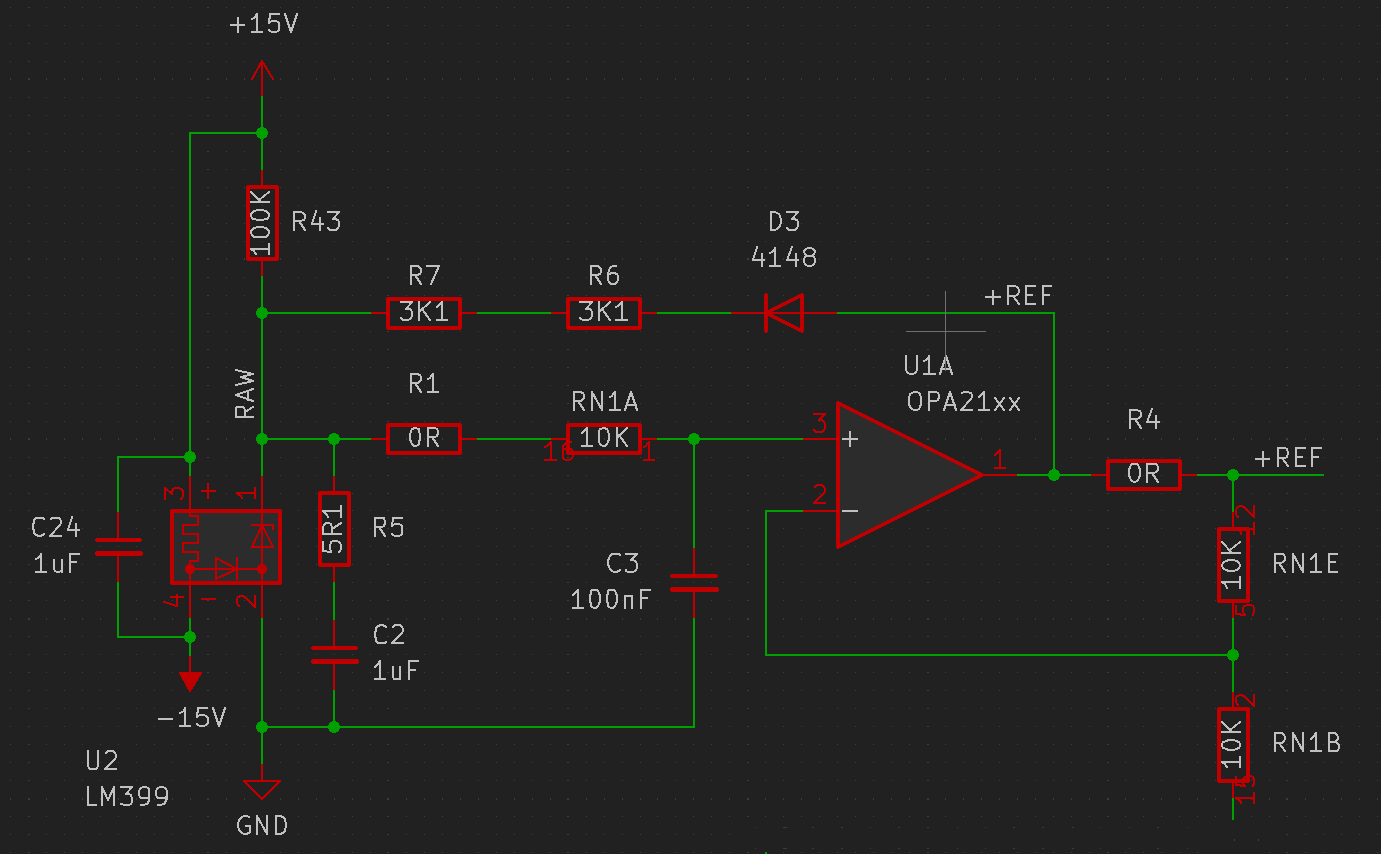
The first thing is the reference voltage. The go-to choice for high-accuracy bench DMMs is the LTZ1000. Given its price, availability and the large number of expensive supporting components required, it is not the best choice for a DIY approach. The LM399 is a popular part that is used in many 6.5 and 7.5 digit meters. It is more or less a simplified version of the LTZ1000 and costs around 20 Euros in single quantity. It consists of a Zener diode and a heater that maintains the diode at a constant temperature. Applying it is very simple, it only needs a heater supply and a current source to bias the Zener diode. The LM399 has now been superseded by the ADR1399.
![]()
Of course, in real life, the LM399 requires a little care and feeding. The heater pins are connected across the +/-15V supply. While starting up, the heater has a low resistance and can easily draw a few hundred milliamps, which can cause the supply voltages to droop. A constant current source could be added in series to the heater to prevent excessive startup current, but on this board I chose not to add an untested circuit. In normal operation, the heater draws around 20mA. The Zener diode is "bootstrapped" to the reference amplifier output. This ensures a constant voltage across the current setting resistors R6 and R7, leading to a stable Zener current and therefore a stable Zener voltage. D3 and R43 form part of the startup circuit to ensure that the reference does not start up the "wrong way", that is, forward biasing the Zener diode. R43 sets up a small trickle current on startup that correctly biases the Zener diode, after which the op-amp takes over through D3. R5 and C2 can be optionally populated if an ADR1399 is being used, which needs some external compensation to ensure good transient response. R1, RN1A and C3 provide some additional filtering to reduce reference noise.
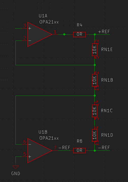
The multislope requires two equal reference voltages of opposite polarity, which are derived from the reference. Feedback resistors could be selected to provide an exact voltage like 10V, but using a 2:1 divider simplifies the overall circuit and gives the input voltage a little more headroom. There are other ways to implement the bipolar references, like a cascaded non-inverting and inverting amplifier, but I chose the "constant current string" topology.
![]()
The LM399's Zener voltage is fed into the input of U1A, which tries to maintain the same voltage across RN1B. Since the other end of RN1B is held at ground by U1B, the voltage across it is exactly the reference voltage. Since RN1E, RN1C and RN1D are of the same value, the same voltage is generated across them since the same current flows through them. This means the outputs of each op-amp are at +/- 2x Zener voltage and inherit some of the LM399's stability.
![]()
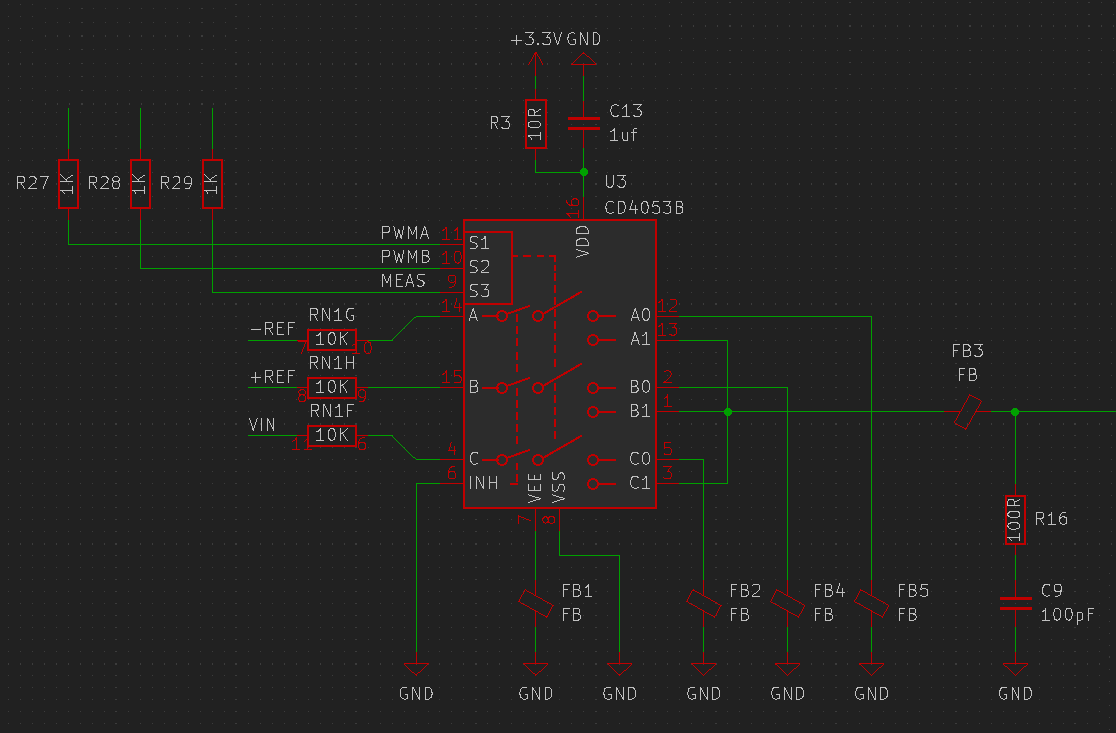
The analog switch is a crucial part of the circuit. My choice was the SN74LV4053 from TI, which is a low voltage variant of the classic CD4053 SPDT analog switch IC. I've tested the LV4053, and it can switch up to several megahertz. Since it can run from a 3.3V supply, talking to it using a Raspberry Pi Pico is easy. The switches in the IC have an on-state resistance of 190 Ohms with a 3V supply and 30 Ohm matching between channels. Temperature coefficient is not specified. It is important that the analog switches have an on resistance that is much smaller than the V-to-I resistors. In this case, the latter are 10 kiloohms, so a 190 Ohm on resistance represents 2% of their resistance. Supposing the switches have a 5%/K temperature coefficient, the overall variation with temperature is just 0.0005%/K (5ppm/K), not including the temperature coefficient of the V-to-I resistors themselves. The ferrite beads prevent switching artefacts from making their way into ground or the summing junction, and the 100R/100pF filter serves to filter charge injection spikes. R27, R28 and R29 prevent the fast rising and falling edges of the control signal from affecting the analog portions of the circuit. Another point to note is that since the reference voltages are approximately +/-14V, an input voltage range of +/-10V or +/-12V is reasonable, and the same resistor value can be used for the reference and input V-to-I conversion.
There is one secret ingredient that helps enhance stability in both the reference amplification and V-to-I conversion sections: the resistors. The reference designator "RN" is already a dead giveaway - the reference amp feedback and the V-to-I conversion resistors are part of the same network. The resistor networks used in most DMMs are custom, but good integrated resistor networks like the LT5400 and NOMCT1603 can be bought for a few Euros each.
Parameter LT5400 (A-Grade, 0C to 70C) NOMC Absolute accuracy +/-7.5% +/-0.1% to +/-1% Ratio accuracy +/-0.01% +/-0.025% to +/-0.1% Absolute temperature coefficient -10 to 25ppm/C +/-25ppm/C Tracking temperature coefficient +/-1ppm/C +/-5ppm/C Excess current noise < -55dB < -30dB The LT5400 clearly wins in terms of ratio accuracy, temperature coefficient and excess noise, but is available only in networks of four, while a single NOMC has 8 resistors, which fits well with the 7 minimum resistors needed to implement a simple multislope. Resistors from the NOMC family also find use in the Keithley 2002 ADC. Nikolai Beev from CERN wrote a comprehensive paper comparing the excess noise performance of various resistor network families. Both the NOMC and the LT5400 have a noise index of less than -60dB.
![]()
Fast slopes require op-amps with a large bandwidth. Fast op-amps are usually not DC accurate, with offset voltages in the millivolt range. An offset voltage on the integrator shows up as a reference mismatch and can affect readings. Precision op-amps usually have poor high-frequency performance. The composite integrator configuration combines both DC accuracy and high speed. The input stage op-amp is of the precision variety, exhibiting low offset voltage. It closes a feedback loop around the fast output stage op-amp to ensure DC precision. The voltage divider acts to reduce the bandwidth of the precision op-amp by requiring a higher swing on its output to drive the non-inverting input of the output stage op-amp. This somehow also has a positive effect on loop stability, which I don't fully understand - more research and testing is needed in this area.
As for the choice of parts, both the op-amps are the OPA140, which is the current voltnuts' choice thanks to low input bias, low input noise voltage, high offset stability, and very good CMRR. They also have a reasonable 11MHz gain-bandwidth product and a 20V/μs slew rate.
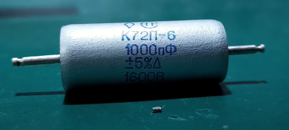
At the center of the whole show is the integrating capacitor. As previously established, reading accuracy depends on the capacitor having low temperature coefficient and low dielectric absorption. This naturally rules out electrolytic capacitors. High-K ceramic capacitors have unacceptably large temperature and voltage coefficients. Film capacitors, particularly polypropylene and polystyrene, are probably the best choice. There is one other rare type of film capacitor that uses a Teflon dielectric, which have the smallest measured dielectric absorption. However, they have very poor volumetric density and are hard to find and therefore very expensive. Low-K ceramic capacitors show marked improvements over their high-K counterparts, and one type, designated C0G, is the best among them. C0G has a 0ppm (+/-30ppm) temperature coefficient, and dielectric absorption almost as low as Teflon capacitors. Most importantly, they are cheap, easily available and small. Here's an 0603 1nF C0G capacitor compared to a 1nF Soviet-era Teflon film capacitor:
![]()
Most multislope ADCs also feature slope amplifiers. As their name suggests, they amplify the integrator waveform, which speeds up the zero crossings. Since the integrator swings between a large range, slope amplifiers are usually diode-clamped. Two variants exist, a non-inverting one with a unity large signal gain, and an inverting one that clamps to +/- one diode drop. The non-inverting type is more common, since it preserves the integrator waveform while speeding up zero-crossings.
![]()
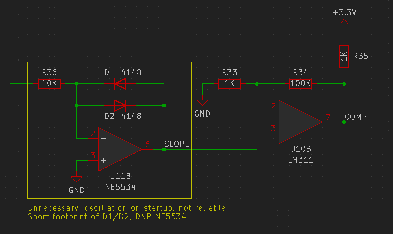
I chose to use the inverting clamping configuration, since I discovered that the LM311 comparator has increased propagation delay when one input is allowed to slew well beyond the reference input. In practice, the circuit I implemented tended to latch up or oscillate, so I ended up bypassing it. The comparator itself, the LM311, is the fastest of the jellybeans, with a 160ns propagation delay. It can also be powered from +/-15V and has a large input common mode range, which simplifies sensing, since no level shifting is needed. A few tens of millivolts of hysteresis also ensures consistent comparison.
![]()
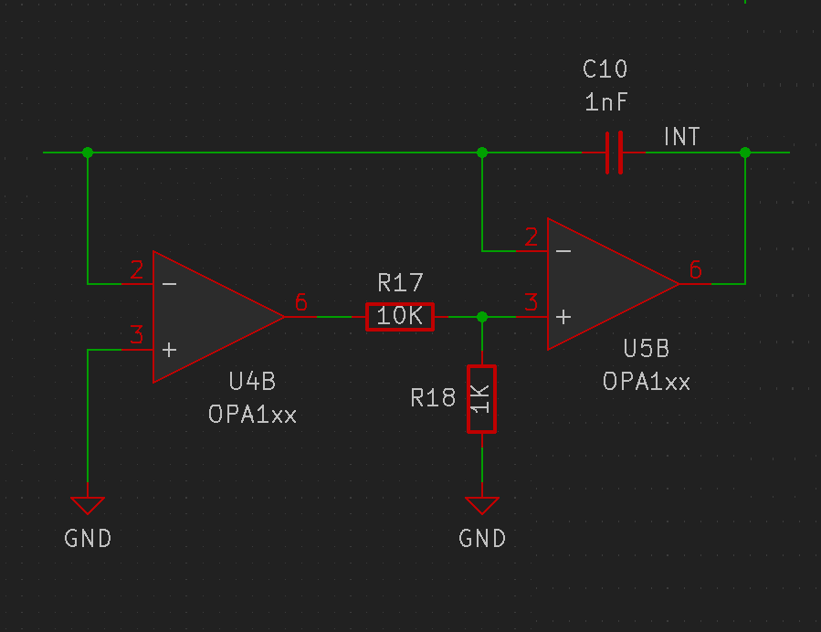
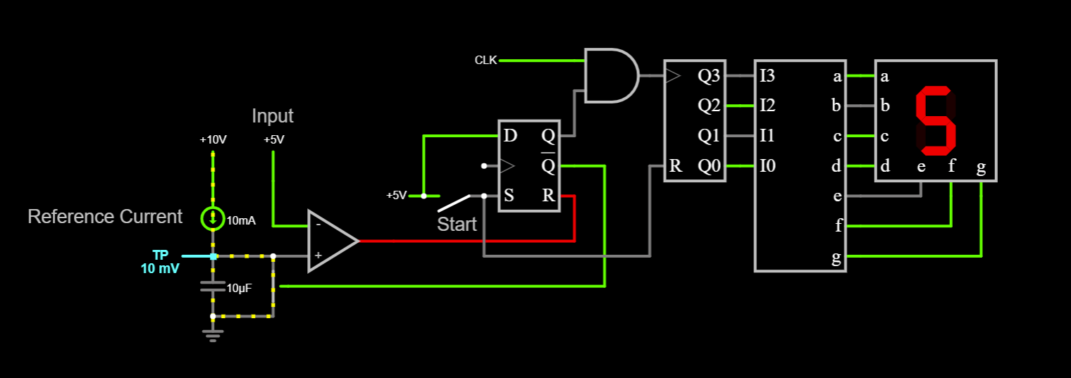
Another powerful technique is being able to measure the actual voltage on the integrator. Even if the input voltage is integrated for one clock cycle, the difference in integrator start and end voltages should still give the correct value for the input voltage. If the integrator voltage is measured before and after a conversion, the difference provides extra resolution to the readings, much like the Vernier scale on a set of Vernier calipers. For this purpose, an MCP3202 ADC is connected to the output of the integrator through a precision scaler that scales the +/-10V integrator swing to 0V - 3.3V that the ADC can digitize. An LM35 temperature sensor (which was designed by the LTZ1000's designer and was his favourite chip) was also added to the second channel of ADC for local temperature measurement.
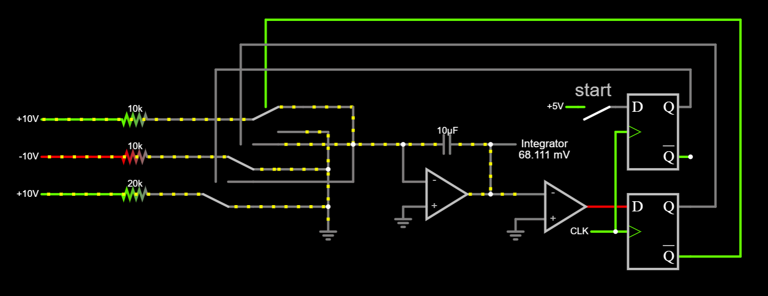
Now that the references, amplifiers, integrator and comparator have been provided, a programmable digital device is needed to close the loop and keep track of the integrator charge. An FPGA or CPLD has traditionally been used to carry out this task. They are also completely alien to me, expensive, and have extensive toolchains. The initial approach Dmytro came up with was to use the SPI hardware on the Arduino Nano, which was strangely suitable in that it generated clock pulses for and read the state of the flip-flop being used to drive the integrator. The only catch was that the SPI transfers could only be one byte long, so every eight clock cycles there was a gap where the integrator charge was not counted.
![]()
The then newly released Raspberry Pi Pico was touted as a solution. It soon became clear that the PIO peripheral was perfectly suited to the task. The D flip-flop could be done away with and the PIO could be used to directly drive the analog switches and also read the comparator output.
One last problem left to solve is that of charge injection. Analog switches are universally based on CMOS processes. The switches are constructed using a complimentary NFET/PFET pair that facilitate bidirectional current flow. Since FET gates are capacitive, the rising edge of the control signal causes a short current spike that makes it to the drain and source terminals, one of which the integrator summing junction is connected to. Every time currents are switched in and out of the integrator, a small unknown charge is added to or subtracted from the integrator. Over many clock cycles, this unknown charge accumulates and causes errors. The non-deterministic nature of the switching and the dependence of charge injection on supply voltage and other conditions makes this error hard to account for.
![]()
There is a clever solution to this problem that dates back to the LD120/121 ADC IC set, whose datasheet also provides insight into multislope operation. This involves using complementary PWM signals to drive the reference switches, with two fixed duty cycle values, for example, 20% and 80%. Regardless of input voltage and integrator levels, PWM provides a constant number of switch transitions. This makes calibrating charge injection errors out a relatively simple process.
![]()
(LD120/121 datasheet, page 3-17, figure 2, 3)
What happens between integration cycles also matters. If the integrator is allowed to drift because of switch leakage, op-amp bias currents or other environmental factors, the output saturates. When the next conversion cycle starts, the integrator takes time to come out of saturation, which affects results. The integrating capacitor's dielectric also soaks up a lot of charge, further affecting readings. Ideally, the capacitor is shorted between conversions, but implementing a shorting circuit is difficult. The HP/Agilent/Keysight 34401A solves this problem by running the integrator constantly, and only counting when a reading is needed. This would be somewhat difficult to implement in PIO, so a different strategy called dithering (described in this paper along with an interesting rundown method) is implemented, which switches the reference currents quickly to maintain the integrator output around zero.
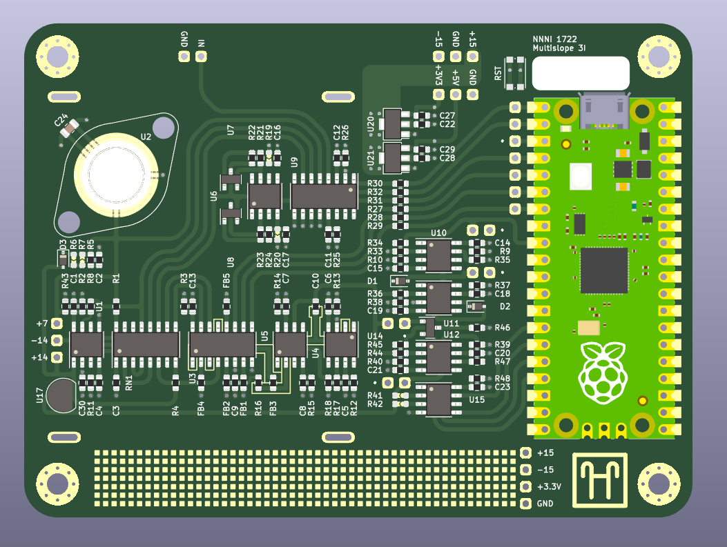
The end result of painstaking testing and debugging was the third iteration of the multislope ADC, called Multislope 3I.
![]()
The PCB layout style was the result of working with Mark on a precision DAC project. I have taken to the neat rows of ICs and passives. Curved traces are electrically unnecessary but result in a product worth looking at. There were surprisingly few teething issues since this was the third PCB I'd made for this project and most of the basic bugs had been ironed out, although a few turned up during testing.
The biggest one came from the MCP3202 residue ADC. The raw output readings were noisy and had significant banding. The reason remains unknown, but PCB layout or a software bug is suspected. This led to the RP2040's built in ADC being used, which reduced noise to a large extent.
The second one involved calibration of conversion constants. If the constants are not chosen correctly, the readings have significant banding. Some fine-tuning using MS Excel fixed the problems.
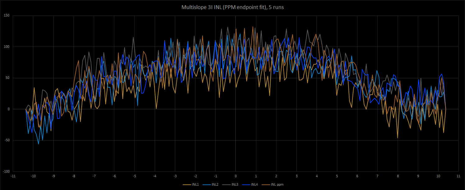
In the time I had to characterize the ADC, I was able to determine that 6.5 digit resolution had probably been achieved, but the readings were quite noisy, and the linearity had an inverted parabolic shape to it. This is a good sign, since the errors is not random and a cause can probably be determined. The spikiness of the data, however, is a bad sign, since it means the readings are quite noisy.
![]()
-
The "Ideal" Multislope Topology
04/11/2023 at 22:26 • 0 commentsI spent a lot of time thinking about how the integrator and current switching circuit topology found in all modern multislope implementations could be improved, but all roads led me back to the same place - the circuit is almost perfect as it is:
The circuit above shows a marked difference from the simulations posted in the previous log. As per tradition, the Falstad simulation of the above circuit is here.
At the heart of the changes is the op-amp based integrator, which takes over from the plain capacitor. In this inverting configuration, the op-amp's inverting input forms a summing junction that is maintained at ground potential. This is one of the main elements that makes precision current switching possible.
Precision floating current sources are quite hard to construct. The Keithley 2002's multislope ADC features such current sources, at the cost of complexity and expensive precision resistors. Since the summing junction is held at 0V, a resistor connected to the summing junction acts like a single component V-to-I converter, with the current into the summing junction being the voltage across the resistor divided by the resistance.
The simple SPST switches have been replaced by SPDT switches. The central pole is connected to the "bottom" of the resistors, one terminal to the summing junction, and one to ground. It might seem like SPST switches would suffice, but if that were the case, the reference voltages (which are usually derived from an op-amp) would see a changing load between 0A and the reference current at several kilohertz. Precision op-amps, which are used to derive the reference voltages, usually have a low bandwidth and cannot respond quickly to load changes. This leads to reference instability and overall measurement inaccuracy. By using an SPDT switch to steer current between ground and the summing junction, a constant current is drawn from the reference voltage. This helps with accuracy and stability. All terminals of the switch are also held at a constant voltage, eliminating to a large extent a crippling parasitic effect present in almost all CMOS analog switches called charge injection.
-
Integrating ADCs: An Introduction
04/11/2023 at 19:54 • 0 commentsIntegrating ADCs fall under the broad category of ADCs that convert voltage to time, which include voltage-to-frequency and voltage-to-duty cycle. The name itself implies that the mathematical function of integration takes place along the conversion process. The most convenient electronic building block to perform that task is the capacitor, the voltage across which is an integral of the input current over time, described by:
Since an integrator is basically a first-order RC filter, most of the high frequency noise on the input is filtered out, leading to cleaner readings. On the other hand, the integrating action also means that conversion times are relatively slow.
The simplest manifestation of an integrating ADC is the single-slope ADC, which consists of a current source feeding a capacitor, a comparator and some controlling circuitry. The input signal is fed into one input of the comparator, and the current source driven capacitor is connected to the other. External circuitry maintains the capacitor at 0V through a shorting switch. When the conversion starts, the shorting switch is opened and the capacitor charges through the current source. Since the charging current is constant, the voltage ramps up linearly. When the voltage across the capacitor equals the input voltage, the comparator signals the control circuitry to stop the conversion. It also shorts capacitor to reset it for the next cycle. The actual conversion from analog to digital takes place at the comparator output, which is a binary representation of the state of charge of the integrating capacitor. This is used to gate a series of clock pulses. The number of pulses is directly proportional to the voltage on the capacitor, and therefore the input voltage.
Here's a link to a Falstad simulation.
Although straightforward, this simplistic method is not without its flaws. Integrating ADCs rely heavily on the integrating capacitor being stable with time and temperature. There is one other undesirable property of capacitors that can affect linearity - dielectric absorption. Increasing precision also places demands on the comparator, which needs to have a low offset voltage and low input noise. Although the absolute value of the offset voltage can be calibrated out, its variation with temperature is harder to account for. Input noise also affects the repeatability of the comparison. The latter effect is practically never mentioned in datasheets and determining it can be trickier than that of op-amps.
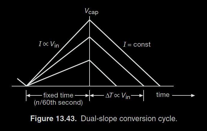
Dual-slope ADCs solve both of these problems to a large extent. A current proportional to the input voltage is allowed to charge the integrating capacitor for a fixed time period. The voltage on the capacitor after this time is proportional to the input voltage. The capacitor is then discharged through a constant current source. The discharge time is proportional to the input voltage and can be digitized in a similar manner as the single-slope.
![]()
(The Art of Electronics, pg. 915 Figure 13.43)
The above diagram from The Art of Electronics explains the dual-slope conversion process.
Since the process now involves two slopes - one to charge the capacitor to a voltage proportional to the input voltage and the other to discharge it down to zero - the effects of dielectric absorption are seen on both slopes and have a smaller effect on the readings. Since the slopes start and end at the same voltage, comparator offset cancels out.
Here's another Falstad simulation of a dual-slope ADC.
The limitations of dual-slope ADCs occur at the higher and lower end of the measurement range. At the lower and, resolution is limited by measurable integrator swing, clock resolution and the noise floor. At the upper end, the integrator needs larger output swings for the larger input voltages, risking saturation. Another subtle disadvantage the dual-slope shares with the single-slope is that measurement time is proportional to the input voltage. In many cases, a constant measurement time is desirable.
So far, the simple examples above contained only one reference current source. With the addition of a single reference current source of the opposite polarity, a multislope ADC can be created. The "multi" in multislope surprisingly does not refer to having multiple current sources/sinks of different values and thus leading to different slopes on the integrator, but to the fact that the two reference slopes are switched alternatively into the integrating capacitor. *
And here's yet another Falstad simulation of a multislope ADC.
The multislope ADC can be thought of as a simple triangle wave oscillator. Assuming zero input voltage and matched reference currents, the output of the integrator is a triangle waveform and the output of the driving flip-flop is a signal with a 50% duty cycle. Compared to the single- and dual-slope ADCs, the multislope is easily clocked. This means each clock cycle injects a fixed positive or negative charge into the integrator.
The input current, once switched into the integrator, causes an imbalance in the charge and discharge currents, and therefore changes the duty cycle of the oscillator. The loop now has to clock charge into the integrator to cancel out the input current. Over a large number of clock cycles, the difference between the amount of positive and negative charge clocked into the integrator is proportional to the input voltage. Even small currents trickling into the integrator over a long time can cause a measurable difference in the positive and negative counts, making this method suitable for measuring very small input voltages.
This continuous charge balancing method is no longer limited by integrator saturation, thanks to being in a closed zero-seeking loop. The integrator can now accept input charge indefinitely, provided the input current does not overpower either reference currents. Constant measurement time can also be achieved by integrating over a fixed number of clock cycles.
A natural extension of this technique is the delta-sigma ADC. I don't fully understand the math behind it, so it's safe to say it's beyond the scope of this project, although with the right number crunching it can still be implemented using the same circuit.
*An interesting side note: the legendary HP/Agilent/Keysight 3458A DMM does have multiple rundown slopes that are switched in, in decreasing slope order to speed up residue measurement.