Close
0%
0%

CMOS Homemade Operational Amplifier

CMOS Homemade Operational Amplifier module and a photo detector using it.

Similar projects worth following
Operational amplifiers using the CMOS process are now widely used because of their low power consumption. Since the insulated gate of MOSFETs in the CMOS op-amps serves as the signal input, their input resistance is extremely large compared to operational amplifiers using bipolar transistors, and their bias current is extremely low. This time, I will explain how I boldly simplified its internal structure and built my own CMOS op-amp module using discrete MOSFETs to deepen my own understanding of its internal operating behavior and applications. I will also present an example of a self-made evaluation unit that allows experimentation with a non-inverting amplifier circuit, and a photo-detector circuit using a transimpedance amplifier.

1-1. Configuration of the CMOS simple discrete operational amplifier

In a previous my project, an experimental op-amp module with five bipolar transistors was introduced, and a similar configuration structure with five MOSFETs is used for this CMOS operational amplifier OPM-03. Because of the limited variety of single MOSFETs available and the fairly large variation in Vth, I thought it would be difficult to bring each internal part to an operating point that would allow overall operation, even if more FETs were used to improve the characteristics. Therefore, in this homemade project, it was decided that even if the characteristics were inferior to those of commercially available monolithic ICs, it would be sufficient if I could manage to achieve operation as a CMOS operational amplifier and experience its features.

    Figure 1 shows the circuit of OPM-03. The internal circuit consists of three stages: the first stage is a differential pair, the second stage is a gain stage, and the third stage is a source follower. The MOSFETs used are 2N7000 for the N-channel type and BS250P for the P-channel type, both of which are for low-power switching. The datasheet states that the Vth value varies from 0.8 V to 3 V.
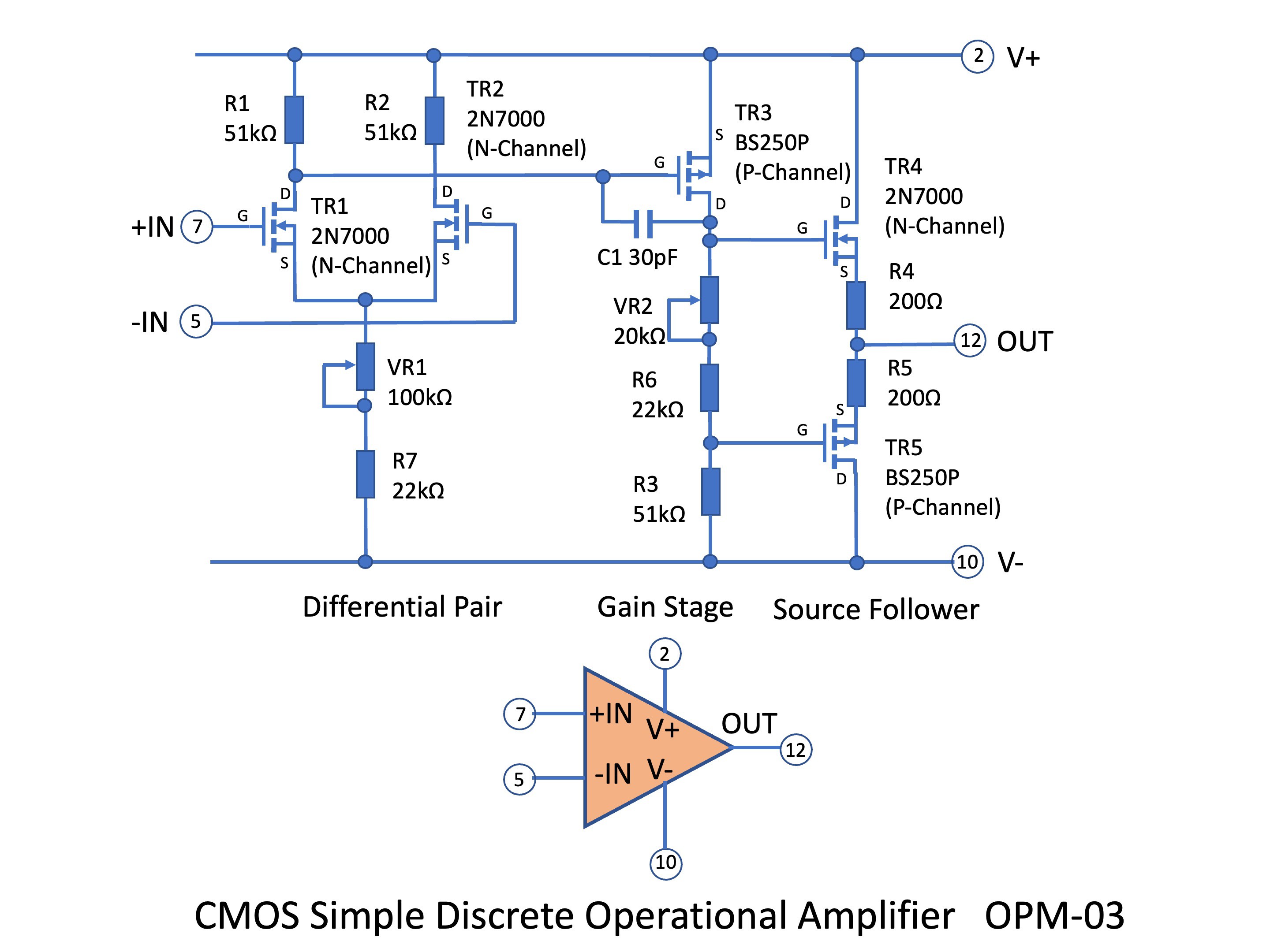
Fig.1 Circuit of the CMOS simple discrete operational amplifier

    Figures 2 and 3 show the appearance of the homemade CMOS discrete operational amplifier. The external dimensions are the same as the op-amp module of the previous project, 30 mm x 30 mm, and the pin layout is the same.
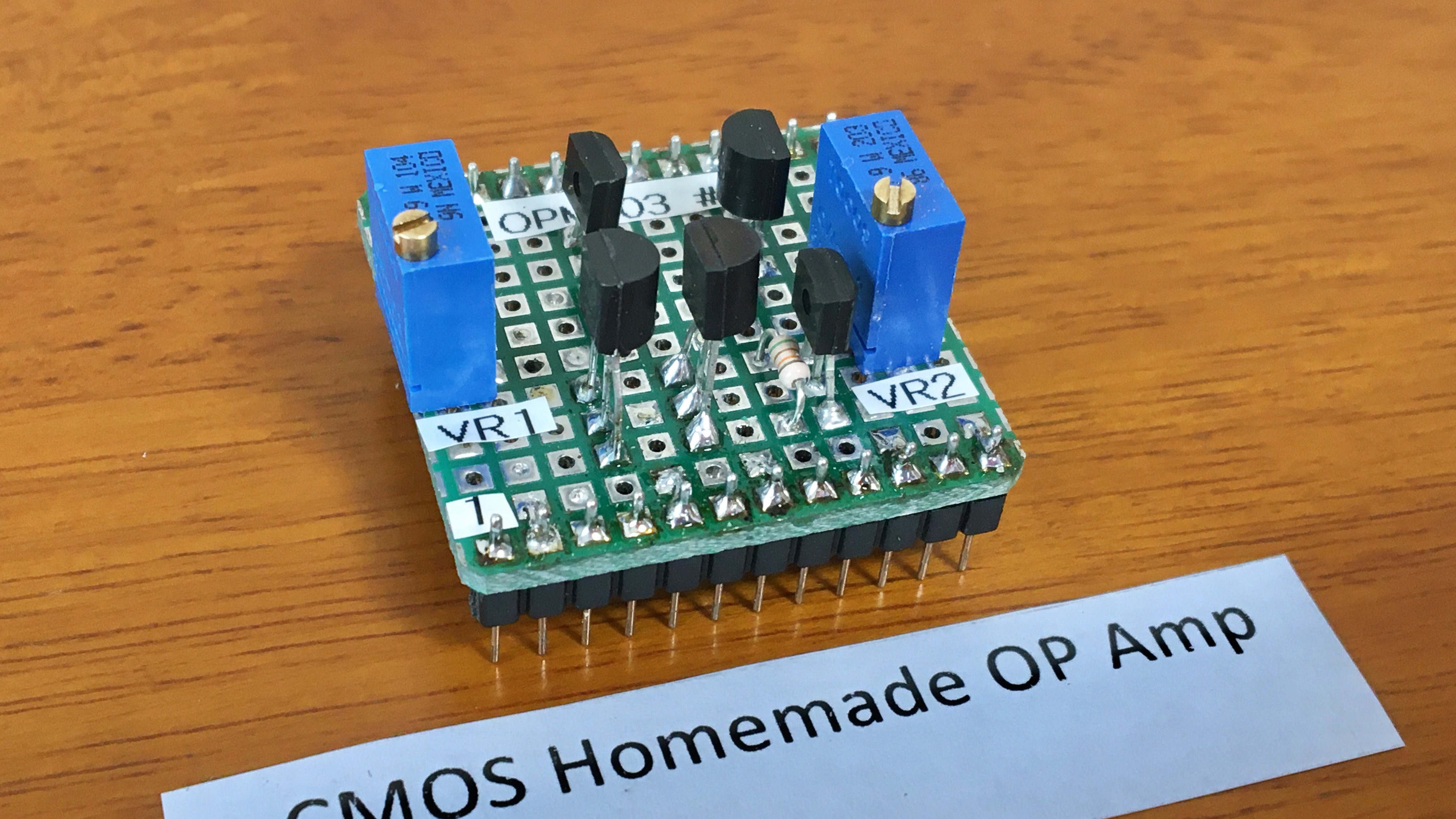
Fig. 2  CMOS simple discrete operational amplifier OPM-03
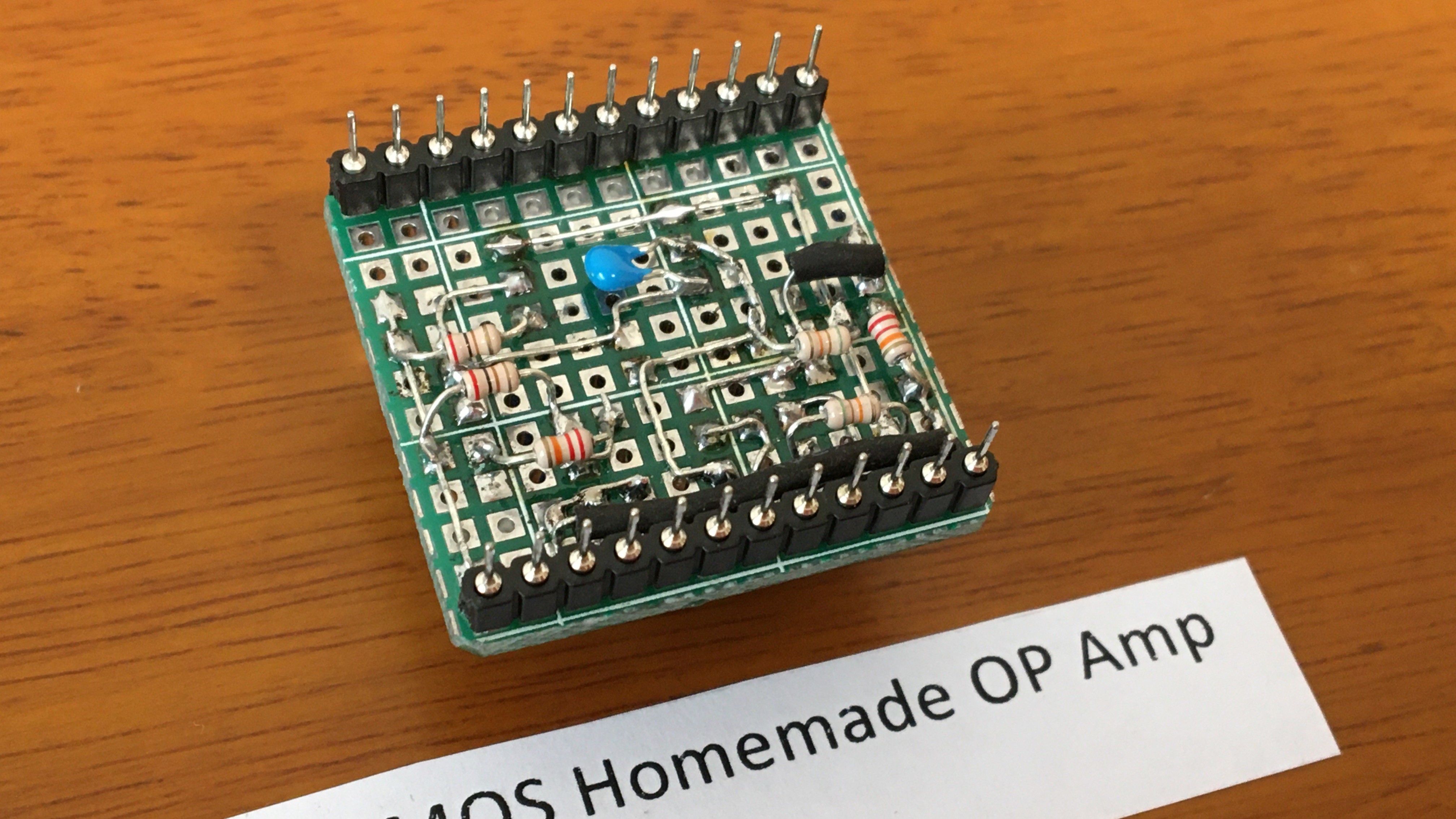
Fig.3  Bottom side of CMOS simple discrete operational amplifier OPM-03

1-2. Differential pair

As shown in Fig. 1, the differential pair consists of TR1 and TR2 N-Channel MOSFETs. The load of the differential pair is the resistors R1 and R2. Typically, a current mirror is used for this load; VR1 and R7 are substitutes for the bias and current sources of a typical differential pair. The drain DC potential of TR1 must be such that the gate potential of the second stage TR3 is operational and the DC offset of the third stage output is zero. It is this VR1 that sets the differential pair operating points so that the drain potential of TR1 satisfies these conditions.

1-3. Gain stage

The gain stage consists only of TR3, a P-Channel MOSFET; C1 is a phase compensation capacitor to prevent parasitic oscillation.VR2, R6 and R3 are the loads of TR3. The potential difference created by VR2 and R6 is to provide a difference in the gate potential of the third stage source follower to eliminate crossover distortion.

1-4. Source follower 

The third stage is a complementary source follower with N-channel MOSFET TR4 and P-channel MOSFET TR5. R4 and R5 are simple protection resistors to limit excessive drain current of TR4 or TR5 in case of output short circuit. However, the power rating of these resistors should be about 2 W. The small resistors pictured in Fig. 3 are not correct.

1-5. Evaluation unit

Figure 4 shows the circuit diagram of the evaluation unit for the homemade discrete operational amplifier module. The non-inverting amplifier circuit, open-loop operation, and photo detector operation with transimpedance amplifier configuration are made possible by toggle switches. The gain can be switched with a rotary switch. Figure 5 shows the inside of this evaluation unit.
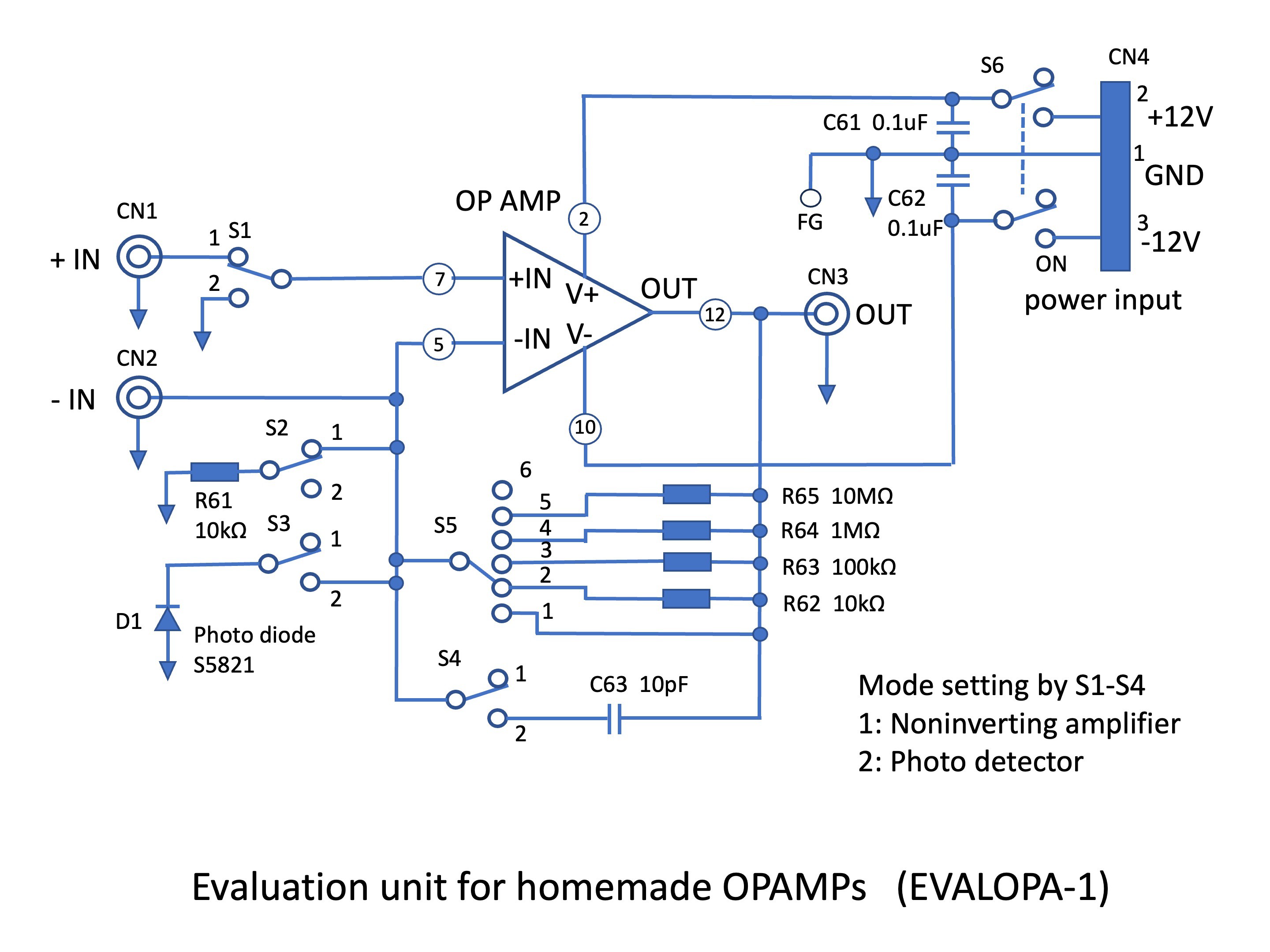
Fig. 4    Evaluation unit for the homemade operational amplifier modules
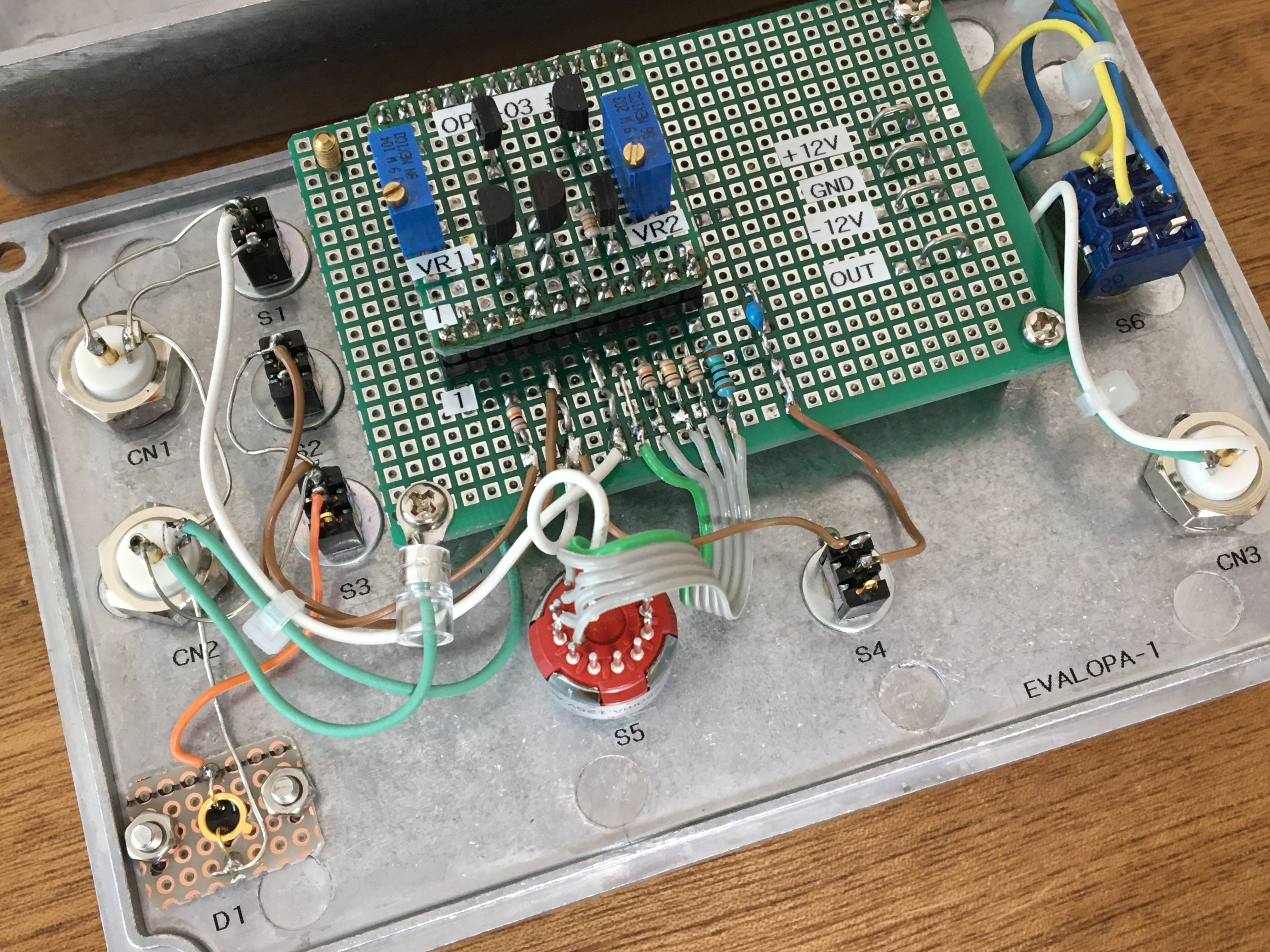
Fig. 5  Inside of the evaluation unit

2. Results

The results of the evaluation of the OPM-03's basic characteristics, non-inverting amplifier, and photodetector operation using this evaluation unit are shown below.

2-1. Result (Operating point)

A typical example of the operating point inside the operational amplifier is 101 kΩ for VR1+R7, +9.01 V for the drain of TR1, and -1.90 V for the source of TR1, under conditions where the...

Read more »

  • 3 × 2N7000 Discrete Semiconductors / Diode-Transistor Modules
  • 2 × BS250P Discrete Semiconductors / Transistors, MOSFETs, FETs, IGBTs
  • 1 × S5821 Opto and Fiber Optic Semiconductors and ICs / Photodiodes

  • OPM-03 project log

    Mitsuru Yamada05/18/2023 at 11:36 0 comments

    1.  The article was first posted on May. 17, 2023.

    2.  Revised on May. 18, 2023.

         Added the Fig. 6 (Open-loop frequency response of OPM-03).

         Added the Chapter 2-7. Power consumption, operating voltage.

    3.  Revised on May. 22, 2023.

         Added description of estimated bias current in Chapter 2-3, Result (Bias Current).

         Corrected the measured value of output variation from maximum 38mV to 70uV in Chapter 3-1, Photo detector Gain linearity.

    4. Revised on May. 29, 2023.

         Corrected the input bias current of OPM-01 from 10 uA to 2 uA in Chapter 2-2.

         Added the frequency response of OPM-01 to Fig. 6 in Chapter 2-3.

         Corrected the output offset voltage of OPM-01 from 800 mV to 1800 mV in Chapter 3-1.

         Added Table 1 for comparison of OPM-03 and OPM-01 in Chapter 4.

View project log

Enjoy this project?

Share

Discussions

s.tamasd wrote 11/11/2023 at 17:44 point

Very cool. I have actually recently made a very similar one. For the input stage I used the same 2N7000, but instead of just resistors for biasing I made a proper current source with a JFET (J310) and a 500ohm resistor to set an operating current of 5mA for the sources of the differential pair. I had initially set the current to 1.25mA with a 2Kohm resistor in the current source, but I have found that the higher current doubles the gain-bandwidth product. And at the top I connected an active load, a current mirror made with 2 PNP transistors (2N4403). I got very good performance from this input stage. I am now waiting for some small signal P-channel MOSFETs to be delivered (VP2106) to do it in the reverse polarity as well since P-MOSFETs are said to give lower input voltage noise. I'll keep the same current source, and use a NPN current mirror instead.

(edit) the 2N4403 were matched in hfe and Vbe down to +/-1mV to make the current mirror as efficient as possible.

  Are you sure? yes | no

Mitsuru Yamada wrote 11/12/2023 at 01:21 point

Thanks for the good information. Looking at the VP2106 data sheet it seems to have similar characteristics to BS250P. I have tried a current mirror as a first stage load, but have not completed experimenting because I cannot easily set the overall operating point. This is an issue I will be addressing in the future. My current impression is that it is a bit difficult to set simple and reproducible circuit constants due to Vth variation when configuring a circuit with multiple single MOSFET elements.

  Are you sure? yes | no

s.tamasd wrote 11/12/2023 at 13:19 point

That is true. At least for the 2N7000 lot that I have, I have found them to have very consistent Vgsth of 1.9V, varying only by a few mV from one to another. I plan on playing with some resistor dividers between the current mirror and the differential pair. Note that I haven't mentioned the output stage I use - that's because so far I haven't made one. :) But the bandwidth-gain product I get from just the input stage is 3MHz.

In non-inverting amplifier configuration, gain of 23 (22K and 1K resistors feedback):

input https://i.postimg.cc/DfYfVJfJ/IMG-20231109-081619.png

output https://i.postimg.cc/GtnWrCff/IMG-20231109-081636.png

Schematic, so far: https://i.postimg.cc/2y9Z9MDX/sch1.png

(edit) with the help of a friend, I have improved the opamp a bit. Now with better CMRR and the provision for adjusting the offset. https://i.postimg.cc/qRqQrWSP/sch3.png

  Are you sure? yes | no

Neal wrote 06/05/2023 at 20:05 point

Very cool project, thanks for sharing it with the world.

  Are you sure? yes | no

Mitsuru Yamada wrote 06/06/2023 at 03:45 point

Thanks! This is a very simple circuit, but it is fun to observe its behavior.

  Are you sure? yes | no

Rudraksha Vegad wrote 05/23/2023 at 22:28 point

That's really interesting homemade OP amp . The soldering is very satisfying ☺

  Are you sure? yes | no

Mitsuru Yamada wrote 05/24/2023 at 00:53 point

Thanks. For me, I enjoy the time I spend doing trial-and-error circuit experiments, replacing circuit elements by soldering.

  Are you sure? yes | no

Kuba Sunderland-Ober wrote 05/23/2023 at 02:15 point

May I ask what software/process do you use to draw the schematics? They are quite stylish - like well made illustrations from some electronics magazine many years ago.

  Are you sure? yes | no

Mitsuru Yamada wrote 05/23/2023 at 05:23 point

Thanks! Schematics for my articles are drawn in Microsoft PowerPoint using only straight lines, rectangles, and circles. Symbols as MOSFETs are also made by grouping shapes. The completed diagrams are exported to JPG. It is a lot of work even for a simple circuit, but I think this is the best way to make everyone feel comfortable reading the article.

  Are you sure? yes | no

Kuba Sunderland-Ober wrote 05/24/2023 at 04:34 point

I agree. You approach this task like an artist would. There's lots of beauty in it - even though it's such a technical subject.

  Are you sure? yes | no

chris wrote 06/06/2023 at 23:57 point

I love this. It reminds me of Rod Elliot (of "Elliot Sound Products") who does his elegant schematics in Microsoft Paint (https://sound-au.com/faq.htm#sch)

  Are you sure? yes | no

Kuba Sunderland-Ober wrote 05/20/2023 at 23:51 point

I will try this with a CD4007. A single-chip homemade op-amp :) Perhaps the matching and tracking of devices on the same die will make life easier. 

  Are you sure? yes | no

Mitsuru Yamada wrote 05/21/2023 at 01:01 point

Thanks! I had inadvertently forgotten about the CD4007 CMOS device for some reason. This is better.

  Are you sure? yes | no

Kuba Sunderland-Ober wrote 05/23/2023 at 02:08 point

The mosfets in the 4007 have fairly low transconductance so that's a big advantage of discrete parts. I wouldn't be surprised if the gain decreased just by going to a 4007. But perhaps input stages in a 4007 would be more stable? I will experiment :)

I have built a current conveyor using a 4007 and to make it work reasonably well several chips have to be connected in parallel to increase conductance.

Here's the circuit before paralleling it:

https://electronics.stackexchange.com/a/614982/10810

  Are you sure? yes | no

Yann Guidon / YGDES wrote 05/20/2023 at 22:41 point

Thanks for the reminder that I still should make one with Germanium transistors ;-)

  Are you sure? yes | no

Mitsuru Yamada wrote 05/20/2023 at 23:45 point

Thank you very much. There seem to be very few articles published on homemade op-amps with CMOS FET configuration, so I took this challenge.

  Are you sure? yes | no

Similar Projects

Does this project spark your interest?

Become a member to follow this project and never miss any updates