Michael Gardi
-
Integrate Panel PCB With Console Application
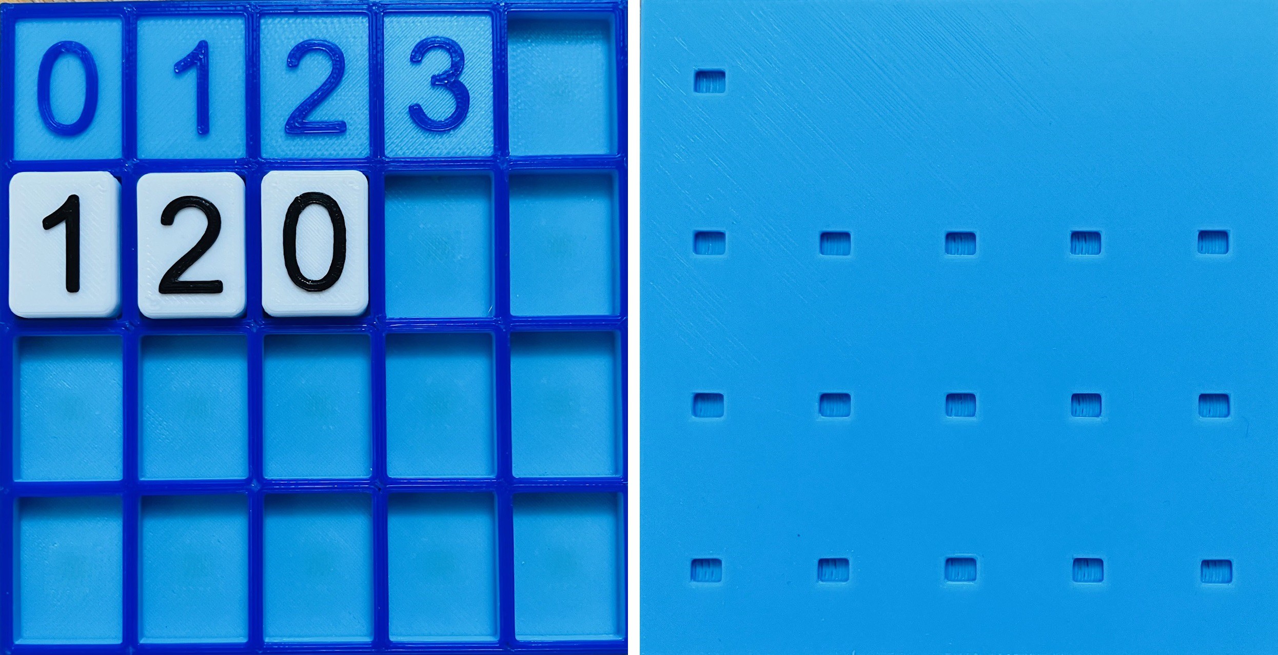
08/20/2023 at 21:49 • 0 commentsI have added code to the TMD-3 Console application to read tiles from my one completed Panel PCB. So the single panel is mapped to the C State of the State Definition Table.
![]()
As you can see from the photo, the integration went well. Just to clarify, when the one READ value is set to 'b' it's corresponding WRITE value is automatically set to 'b' as well since 'b' (a boundary condition) cannot be overwritten.
I have uploaded the new code on github. Note that the Console application will still run in an environment that does not have tile hardware (in software only mode). I'll post a video of the tile panel in action and the PCB's KiCad files soon.
-
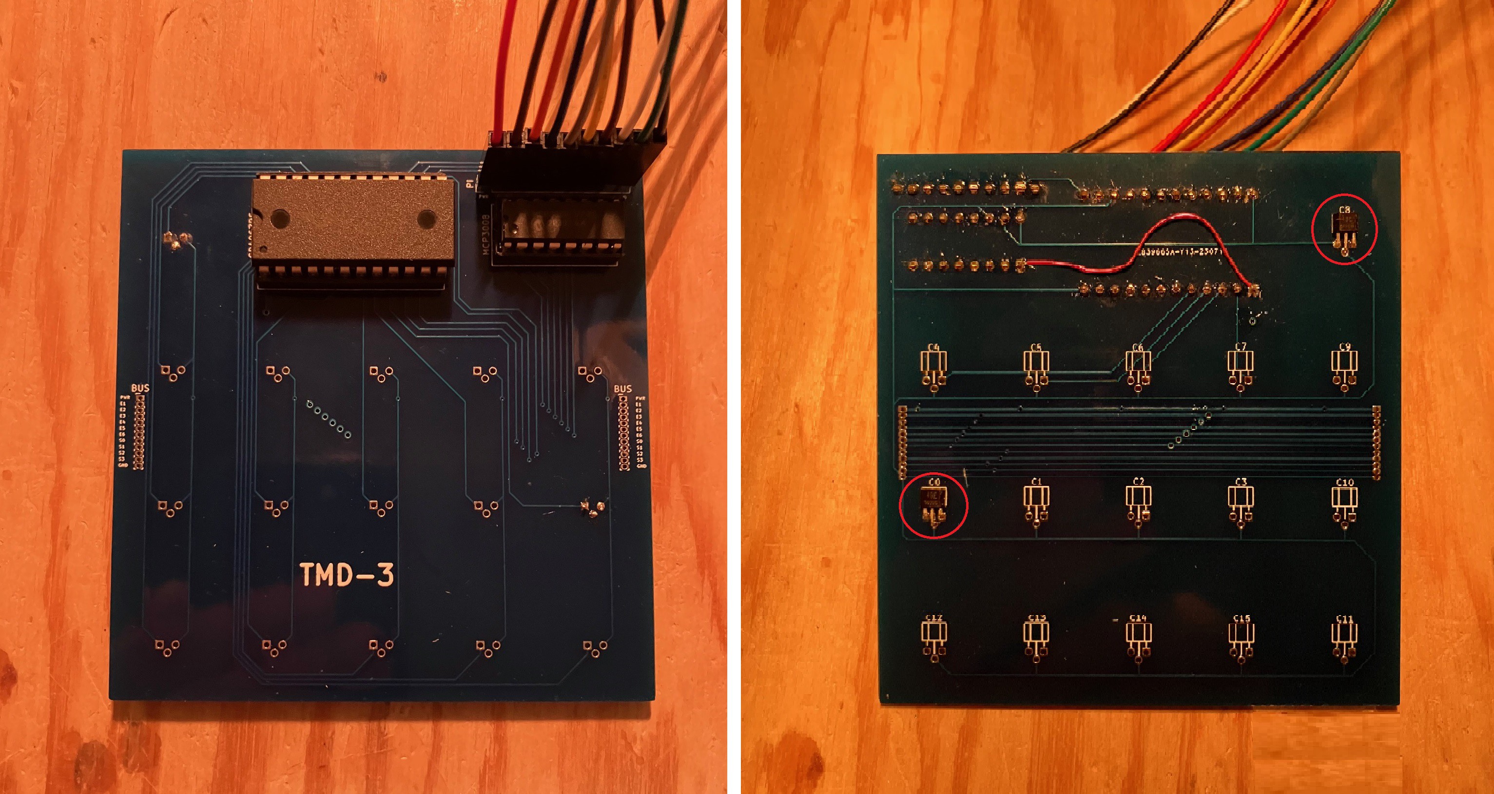
Testing the Fully Populated State PCB
08/18/2023 at 17:44 • 0 commentsI finally got around to fully populating the state table PCB. Using the technique posted in a previous log, I carefully soldered the 16 linear hall effect sensors, then the header, multiplexor, and ADC chips to the board.
![]()
Remember that the red wire is to connect the primary input/output pin of the multiplexor to channel 0 of the ADC for this board. The other 5 boards forming the state transition table will be wired individually to channels 1-5 of this same ADC via the “bus”. I have added the sensor numbers as labels to the PCB photo for clarity. I also added the rectangular indentation to the bottom of the printed panel to accommodate the soldered pins of the ICs and header as I found that the panel would not sit flush against the PCB and sensors otherwise.
First I wanted to test the variance between sensors. I wrote a small script to measure each of the sensors in turn. Things to note:
- The script is initialized by recording the "at rest" (no magnetic field) reading for each sensor. As has been stated the sensors initially read in the middle of the range of possible values.
- If a reading varies from this initial value by more than 200, the sensor number and the value read is output.
- The emitted value is the raw reading minus the mid point value divided by 100 and rounded to the nearest integer.
import time
import busio
import digitalio
import board
import adafruit_mcp3xxx.mcp3008 as MCP
from adafruit_mcp3xxx.analog_in import AnalogIn
import pigpio

# Access the gpio pins.
GPIO = pigpio.pi()

# Select pins for the CD4067BE.
S0 = 23
S1 = 27
S2 = 17
S3 = 18

# Selct pins are all OUTPUT.
GPIO.set_mode(S0, pigpio.OUTPUT)
GPIO.set_mode(S1, pigpio.OUTPUT)
GPIO.set_mode(S2, pigpio.OUTPUT)
GPIO.set_mode(S3, pigpio.OUTPUT)

# Select the C8 pin.
GPIO.write(S0, 0)
GPIO.write(S1, 0)
GPIO.write(S2, 0)
GPIO.write(S3, 0)

# Create the spi bus.
spi = busio.SPI(clock=board.SCK, MISO=board.MISO, MOSI=board.MOSI)

# cCreate the cs (chip select).
cs = digitalio.DigitalInOut(board.D22)

# Create the mcp object.
mcp = MCP.MCP3008(spi, cs)

# Create an analog input channel on pin 0.
chan0 = AnalogIn(mcp, MCP.P0)

def selectPin(pin):
    if pin & 0b00000001:
        GPIO.write(S0, 1)
    else:
        GPIO.write(S0, 0)
    if pin & 0b00000010:
        GPIO.write(S1, 1)
    else:
        GPIO.write(S1, 0)
    if pin & 0b00000100:
        GPIO.write(S2, 1)
    else:
        GPIO.write(S2, 0)
    if pin & 0b00001000:
        GPIO.write(S3, 1)
    else:
        GPIO.write(S3, 0)

# The hall effect sensor will read in the middle of the range
# someplace. Get the middle values for all 16 sensors.
mids = []
for i in range(0,16):
    selectPin(i)
    time.sleep(0.01)
    mids.append(chan0.value)
print(mids)

while True:

    for i in range(0,16):
        selectPin(i)
        time.sleep(0.01)
        val = chan0.value-mids[i]
        if abs(val) > 200:
            print("C",i,"=",round(val/100))
    time.sleep(0.5)
For each magnet distance from 1 mm to 4 mm I recorded the values from all 16 sensors. The same magnet was used for all readings.
C0 C1 C2 C3 C4 C5 C6 C7 C8 C9 C10 C11 C12 C13 C14 C15 1 mm 52 49 47 49 52 49 48 50 56 52 50 53 58 51 49 51 2 mm 31 29 29 29 31 29 29 30 33 31 30 31 33 30 29 31 3 mm 22 21 20 20 22 21 20 21 23 21 21 22 24 21 20 22 4 mm 14 13 13 13 14 13 13 14 15 14 13 14 15 13 13 14 I was pretty happy with the results. For each distance the values grouped fairly well although I would note that the difference between the lowest and highest values read was worst for the 1 mm values (11) but got better as the distance increased, 2 mm difference (4), 3 mm difference (4), and 4 mm difference (2).
In a second set of tests, for each distance, I measured the values returned from 10 different magnets. In all cases the C0 sensor was used.
M1 M2 M3 M4 M5 M6 M7 M8 M9 M10 1 mm 35 49 52 51 53 52 51 51 51 49 2 mm 22 31 33 32 31 32 31 31 31 30 3 mm 15 15 22 19 22 22 22 22 22 21 4 mm 10 13 14 13 13 13 13 13 13 10 Again fairly good grouping although I have highlighted a number of cases where the value for a particular magnet diverged quite a bit from the "norm". The magnets that I am using are cheap and suspect not even neodymium. To try and mitigate these divergences, I have ordered some better neodymium magnets from a reputable dealer.
Although it will be a pain in the butt, I suspect given these findings that for the best results I may have to calibrate each sensor against the all tiles that will be placed at that position. We'll see. The good news it that I should only have to do this once.
-
The Perils of PCBing Without a Net
08/05/2023 at 05:12 • 1 commentI have a confession to make. I created the state PCB for TMD-3 directly in the KiCad PCB editor without creating a schematic first. This is pretty easy to do. Of course I had to turn off DRC to accomplish thus but hey I figured I was saving myself some time. Wrong.
![]()
I missed introducing a small trace when converting the bus connectors to standard .1 inch headers and inadvertently crossed the S2 and S3 lines. Took me a while to find the problem that a netlist and DRC would have probably caught.
Fortunately the boards could be salvaged with a delicate but doable trace cut.
Lesson learned.
-
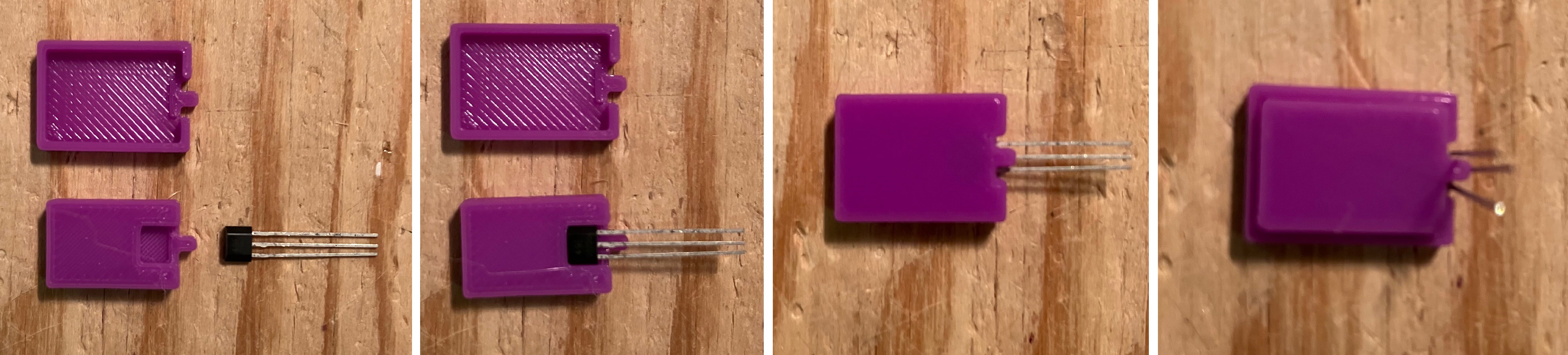
Mounting the Hall Effect Sensors
08/02/2023 at 15:41 • 0 commentsAs I add the Hall Effect Sensors to the PCB, I am trying to position them as consistently as possible to each other so that the readings from different sensors are the same. The first step is to bend the leads on the sensors in a uniform way. To that end I designed and printed a little jig.
![]()
The sensor is placed into the indentation in the lower part of the jig, then the upper part is positioned on top as seen in the third photo above. With the sensor firmly in place, the jig is flipped and the three leads are carefully bent up 90 degrees.
To mound the sensor onto the PCB I first applied a small piece of two sided tape. (Apologies for the poor quality of the photos that follow.)
![]()
Then when the sensor is slid into place aligned with the square printed onto the PCB, it will be held securely so that it can be soldered.
-
A Tile System
07/24/2023 at 22:31 • 0 commentsFor TMD-1 the nine different tiles were created with the magnets embedded into the tile itself. This was accomplished by defining magnet sized voids inside the tiles and pausing the 3D print at the appropriate time to insert the small magnets. This task was simplified by the fact that the voids were all at the same depth within the tile, plus the polarity of the magnet was not relevant, so a big batch of different tiles could be created at the same time.
There were no magnets in TMD-2 so printing them was pretty straight forward.
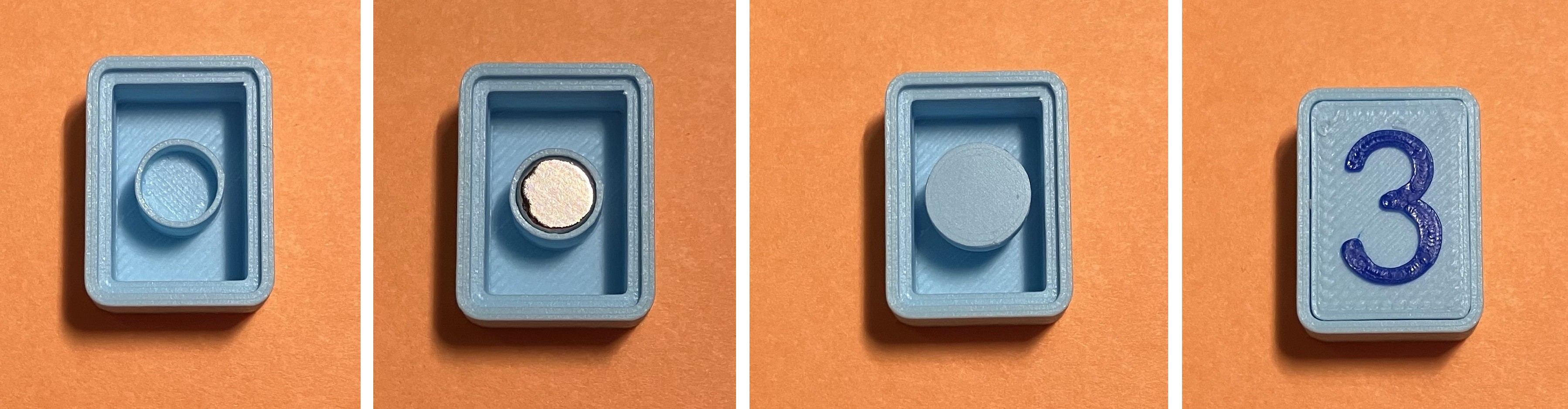
For TMD-3 the sixteen different tiles will have the magnet voids at different heights depending on the tile, so smaller batches would be required when printing.
I thought I might make the job a bit easier by assembling tiles from pieces. That way I can print the parts in larger batches. Here is what I am thinking.
![]()
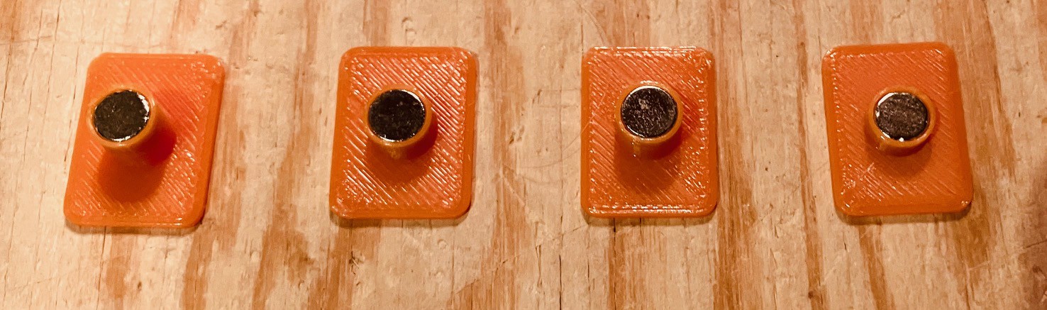
We start on the left with a tile base. There will be four different types of these with the magnet pedestals at different heights (1 mm to 4 mm). The magnet is placed on the pedestal and held in place with a printed cap. Finally the tile face is snapped in place. All of these pieces can be printed in large batches and assembled later.
Once I had the "system" in place I decided to make a complete set of tiles to test with. I printed the bases in one batch, the tops in another (with a pause to change filament), and the caps in a third print run.
![]()
The caps an tops fit pretty snugly, but still needed a drop of glue to set them in place. I used Gorilla Super Glue with the "Micro Precise" applicator which really helped administer the very small amounts of glue necessary.
My next step is to figure out the best way to determine the appropriate measurement settings necessary to recognize the differences between tiles. Will I need to have a "calibration" set when setting up the state transition table? I guess I'll find out.
-
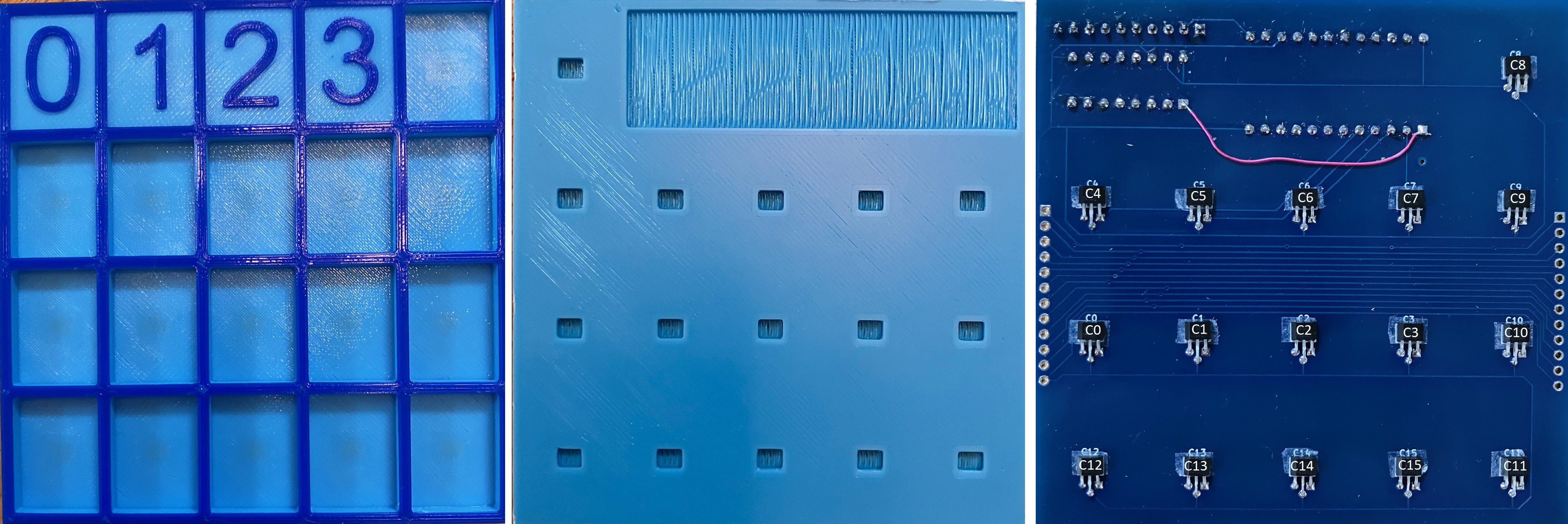
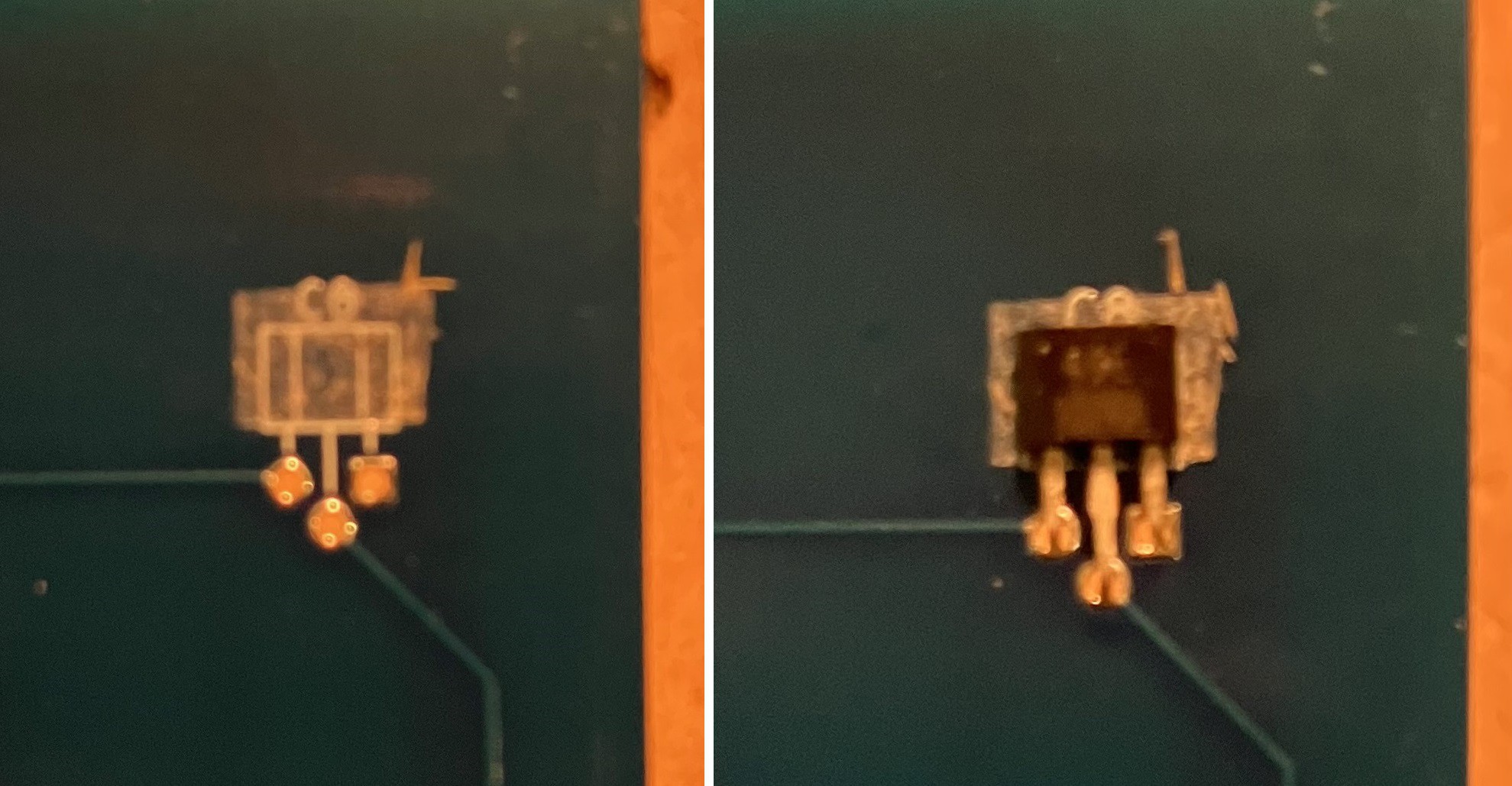
Testing The PCBs
07/23/2023 at 23:04 • 0 commentsThe PCBs arrived from the fab and I was anxious to check them out so I wired one up.
![]()
On the left is the top of the PCB with the CD4067BE multiplexer (large chip), MCP3008 8-channel A/D converter (small chip), and a 10 pin header installed. On the right you can see that I have installed a couple of the SS49E linear hall effect sensors to test with on the bottom of the PCB. Also note that the red wire is not to fix anything, it assigns the common output of the CD4067BE on this state PCB to the channel 0 (C0) pin of the MCP3008. Each of the other 5 state CD4067BEs will be similarly wired to channels 2 through 5 (C2-C5) of the MCP3008.
I wired the header on the PCB to my Raspberry Pi 4.
State PCB Header Raspberry Pi 4 Description PWR 3.3V Power S3 GPIO 18 These 4 pins select one of 16 input channels on the CD4067BE multiplexer. S2 GPIO 17 S1 GPIO 27 S0 GPIO 23 CLK SCLK These 4 pins are used to establish an SPI connection to the MCP3008. DOUT MISO DIN MOSI CS GPIO 22 GND GND Ground I made some test tiles that accept 6 mm x 3 mm round magnets at four different distances from the bottom of the tile (1 mm to 4 mm).
![]()
I wrote a little Python script to test the board.
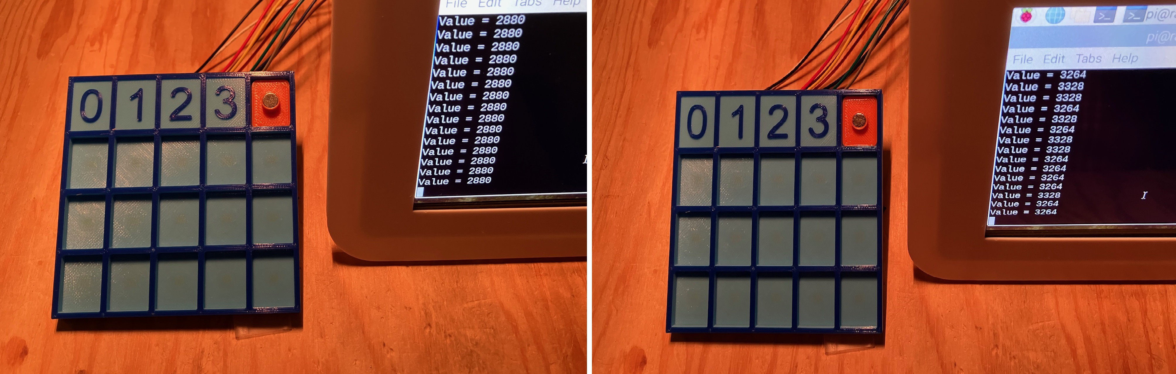
import time
import busio
import digitalio
import board
import adafruit_mcp3xxx.mcp3008 as MCP
from adafruit_mcp3xxx.analog_in import AnalogIn
import pigpio

# Access the gpio pins.
GPIO = pigpio.pi()

# Select pins for the CD4067BE.
S0 = 23
S1 = 27
S2 = 17
S3 = 18

# Select pins are all OUTPUT.
GPIO.set_mode(S0, pigpio.OUTPUT)
GPIO.set_mode(S1, pigpio.OUTPUT)
GPIO.set_mode(S2, pigpio.OUTPUT)
GPIO.set_mode(S3, pigpio.OUTPUT)

# Select the C8 sensor.
GPIO.write(S0, 0)
GPIO.write(S1, 0)
GPIO.write(S2, 0)
GPIO.write(S3, 1)

# Create the spi bus to the MCP3008.
spi = busio.SPI(clock=board.SCK, MISO=board.MISO, MOSI=board.MOSI)

# Create the cs (chip select).
cs = digitalio.DigitalInOut(board.D22)

# Create the mcp object.
mcp = MCP.MCP3008(spi, cs)

# Create an analog input channel on pin 0.
chan0 = AnalogIn(mcp, MCP.P0)

# The hall effect sensor will read in the middle of the range someplace.
mid = chan0.value

while True:

    # read the analog pin
    time.sleep(0.5)
    print('Value =',chan0.value-mid)
When I first tried this script I found that the C8 sensor was not being selected. Ultimately I discovered that the S3 input on the CD4067BE multiplexer was not going high because the pin had been inadvertently tied to ground. Once fixed (by cutting the offending trace) I got good results.
![]()
On the left a "tile" with the magnet 2 mm from the bottom, and on the right the magnet is 1 mm from the bottom. You can see that I am getting pretty good results as the Hall effect sensor readings are quite a distance apart so it should be easy to differentiate between tiles.
I'm going to make another pass at the PCBs to fix the problem I had with the S3 input. Also seeing the PCBs I realize that the pitch on the BUS connectors is way to small to easily run wires between them. I'm changing the connectors to be standard .1 inch headers.
![]() The updated PCB gerber files have been submitted to the fab.
The updated PCB gerber files have been submitted to the fab. -
The State Panel
07/18/2023 at 15:55 • 0 commentsI have decided to keep roughly the same form factor for the State Definition Table input area as I did with the TMD-2 machine. Mostly that means that I am going to keep the same tile size (but not necessarily the same tile thickness). The tiles have a good "feel", but I fear that if they were any smaller (in the interest of making a more compact machine) that would not be the case.
![]()
So I designed and printed just the tile input area for a single state to test with. On the left above you can see the top of this panel with a few TMD-2 tiles for reference. On the right the back of the panel is shown with indentations to accept the SS49E Linear Hall Effect Sensors which will be protruding from the state PCB (which is exactly the same size as this panel).
I'm hoping that enforcing this precise alignment will ensure that I get consistent measurements from each of the sensors. Only testing will tell. It would be inconvenient but not too terrible if I had to calibrate the sensors for each panel to get good results. We'll see.
-
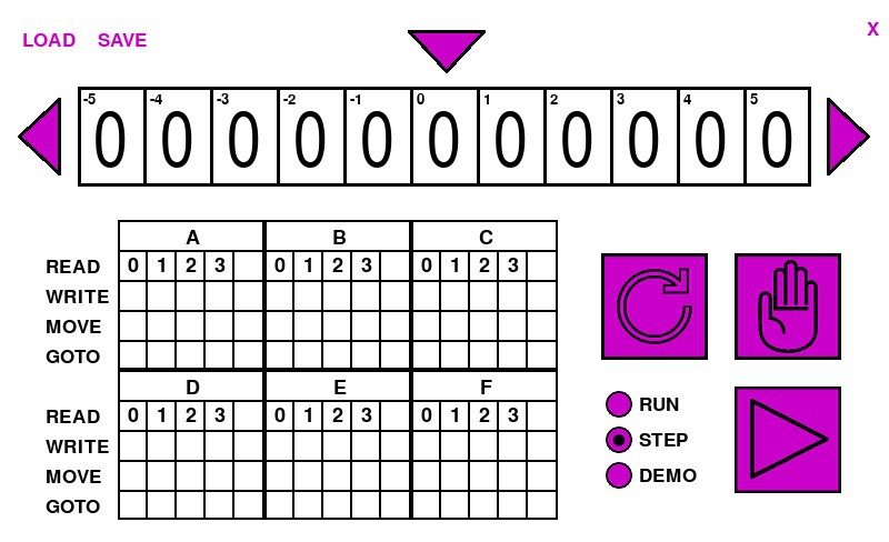
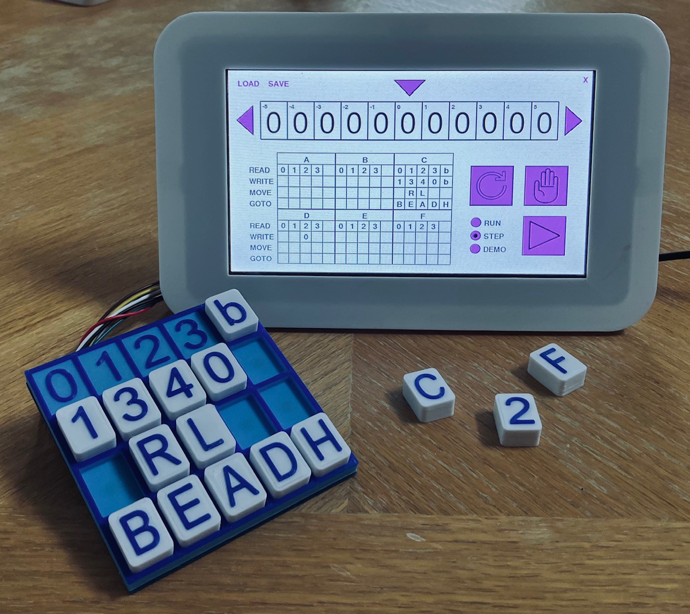
Updated the TMD-3 Console Application
07/17/2023 at 01:51 • 0 commentsWhile I'm waiting for the state PCBs to arrive I have been working on the TMD-3 Console application.
![]()
The biggest change is that the TMD-3 application has been updated to support the new 6-State 5-Symbol specification for Mark 3.
In addition I have created a TMD-3 version of my Quick Start Guide.
Both the application and guide can be found on GitHub.
I want to emphasize something here. While my goal in this project is to make another funky tile based interface for this Turing machine, the console software is completely functional and standalone right now. Because it's written in Python it should run on virtually any Python capable machine. You can download the console software and use the Quick Start Guide to learn all about the concepts behind a Turing machine. The Quick Start Guide includes:
- an overview of Turing machines
- description of the TMD-3 implementation and how it works
- a step-by-step walkthrough of setting up a simple TMD-3 "program"
- some additional "programming" challenges that you can try
- some information about a special class of Turing machine programs, "busy beavers"
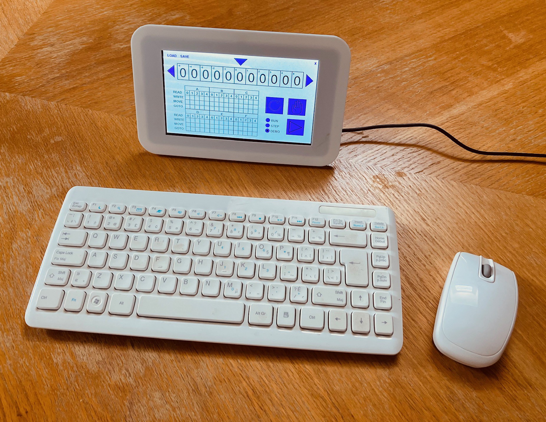
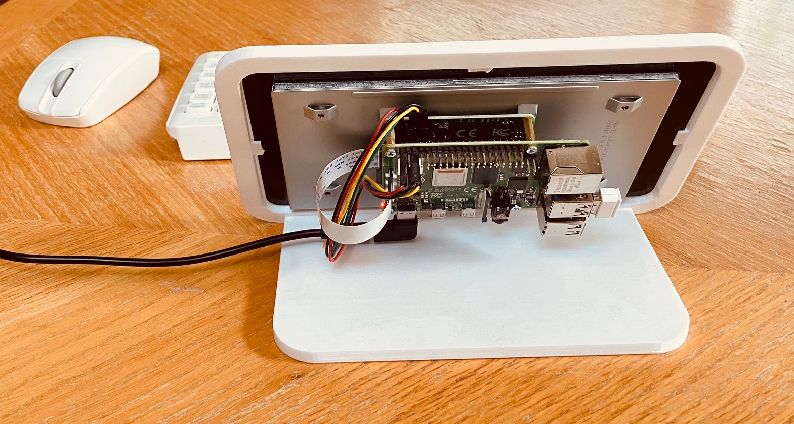
Here is the setup I am using right now to test the console application.
![]()
What you see here is a 7" Raspberry Pi touchscreen display which has a Raspberry Pi 4B attached. I'm using the one from my TMD-2 project.
![]()
The wireless mouse and keyboard are for convenience only as the console application can be completely run with the touchscreen alone.
Speaking of the application running, here is an example of the TMD-3 console running a 3-State 2-Symbol "busy beaver" program on my Windows machine. The busy beaver "game" consists of designing a halting, binary-alphabet Turing machine which writes the most 1s on the tape, using only a given set of states, in this case 3.
In the video you will see the busy beaver "program" being loaded from disk and the console placed in Demo mode so you can see the steps as the program executes.
The result here of six 1s is known to be the maximum that a 3-State busy beaver can attain. A 4-State busy beaver can write at most 13 1s to the tape. At present the largest number of 1s that has been recorded for a 5-State busy beaver is 4098, but here's the thing, the exact maximum result has not yet been found! It is unlikely that the maximum number of 1s for a 6-State busy beaver will ever be found.
This is just one example of the interesting things that you can do with your very own Turing machine. I would encourage you the check out the TMD-3 console and maybe even work through some of the problems in the Quick Start Guide. If you do give it a shot I would appreciate any feedback on how the application and/or the manual could be improved. Thanks.
-
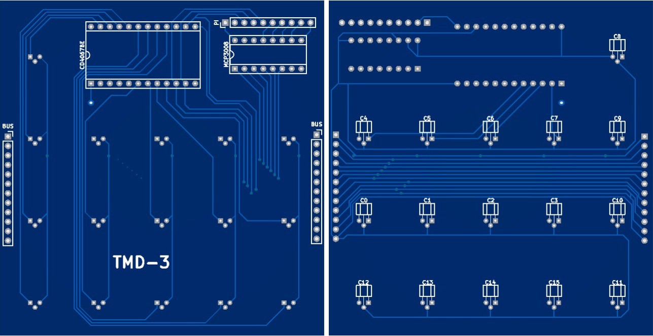
PCB Designed
07/10/2023 at 20:57 • 0 commentsI finished the design for a single state PCB that will manage 16 tile reading SS49E Linear Hall Effect Sensors. Six of these boards will be daisy chained together to complete the state transition table for TMD-3.
![]()
The top of the board is on the left and the bottom on the right. All hall effect sensors will be mounted on the bottom, while each of the six boards will have a CD4067BE 16 channel analog multiplexer installed on the top. Only one of the boards will have the MCP3008 ADC chip and a header to interface with the Raspberry PI installed on the top as well.
PCB design submitted to fab and the chips have been purchased.
TMD-3: Turing Machine Demonstrator Mark 3
They say that the third time's a charm. Let's find out.

 The updated PCB gerber files have been submitted to the fab.