 Arya
Arya-
Depanelizing boards
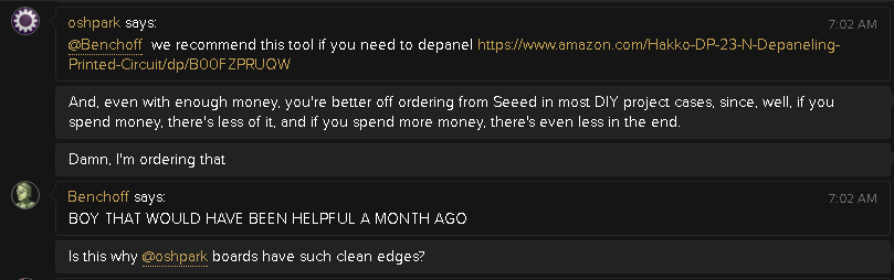
08/03/2017 at 04:07 • 0 commentsI know, I know, this is not #Hackaday.bash.org , but still:
![]()
![]()
![]()
Link to the tool in question ("Hakko CHP DP-23-N Depaneling Tool")
-
Gerber export tutorial - KiCad (with important notes)
06/08/2017 at 02:20 • 0 commentsIMPORTANT
Currently, KiCad-designed boards have origin point problems. This manifests as board appearing outside the outline upon drag&drop, thus, "not geting added" (though it's there).
![]()
To fix this, add an "origin point for drill and pick&place files" (badly named, for sure). This guy over at KiCad forums places it in the upper left corner of the boards, I confused left and right for a second, so the picture shows me being about to place it in the upper right corner:
After that, you can export Gerbers and don't worry about them "disappearing".![]()
Here's my usual gerber generation workflow in KiCad:
- Open PCB in CvPCB
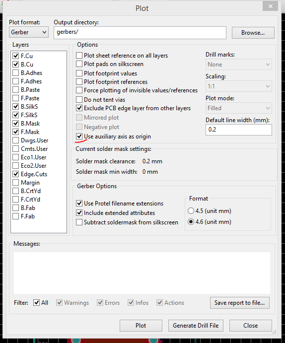
- Menu -> Plot
I use these settings for Gerber plotting:
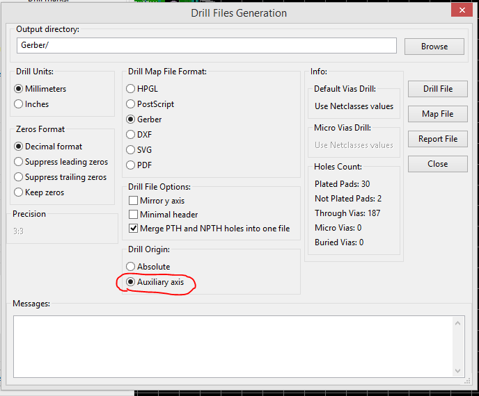
Note the "auxiliary axis" setting, it's necessary for proper export![]()
Then press the "Generate Drill File" button and generate a "Drill File". Here are the settings I used, the one you absolutely need is circled red:
![]()
-
Small PCBs - Logic probe (untested)
05/09/2017 at 00:35 • 0 comments![]()
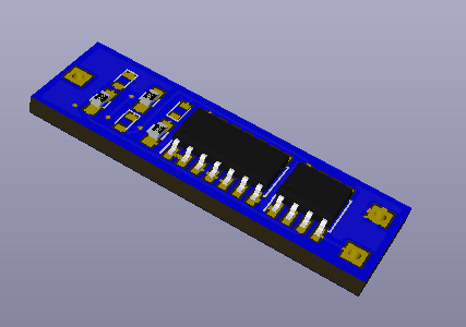
This logic probe design was featured on Hackaday.com blog, and I was interested in assembling a couple of those. So, I made a quick KiCad board that'd be as small as possible - and in the end, it's very very small, using SMD components - but still hand-solderable =) I figure that if you'll want to use this probe on 3.3V designs, you'll want to use a 3.3V-compatible version of 555 IC.
GitHub link (Gerber ZIPs are also there)
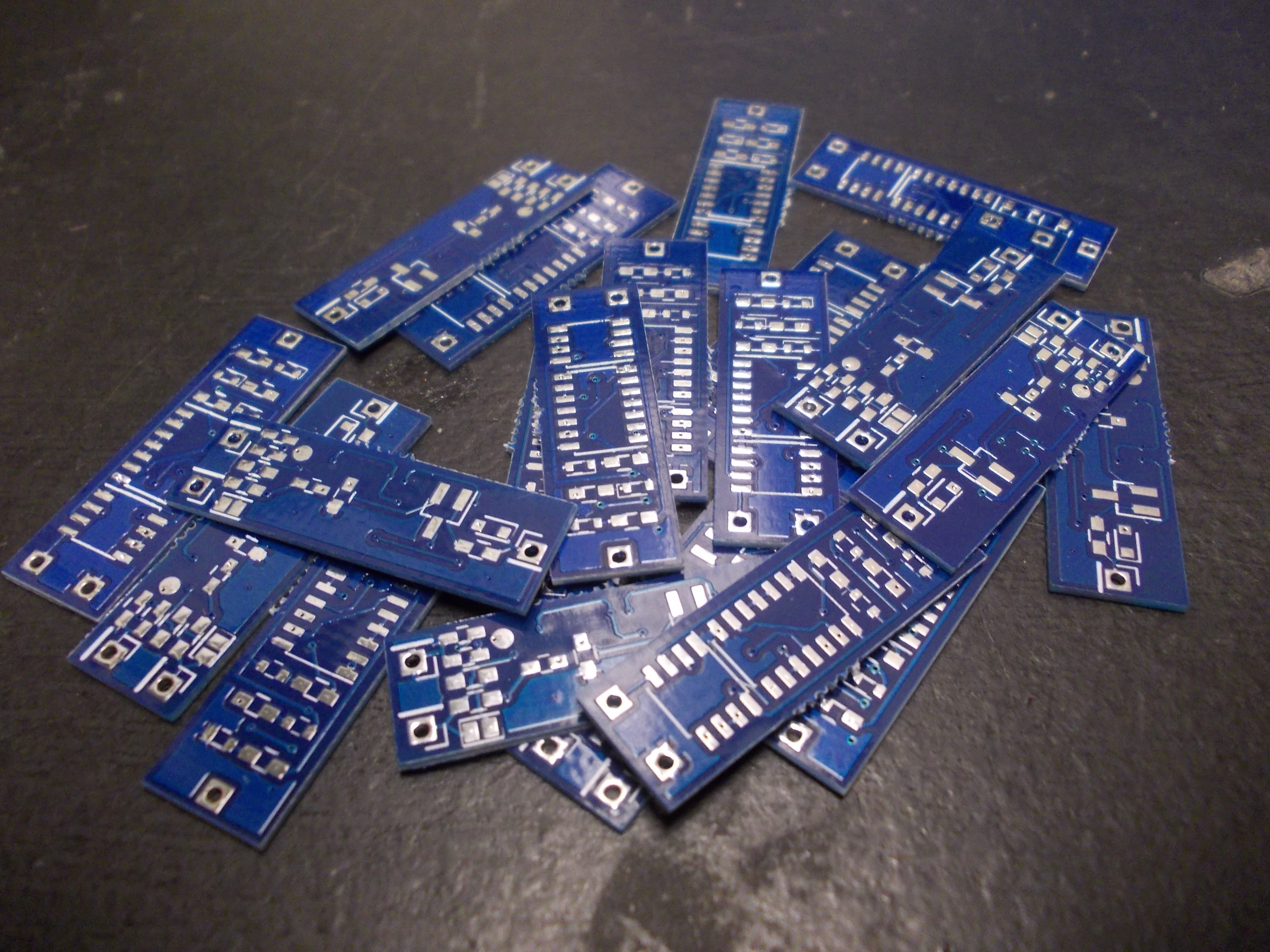
UPDATE: Got the PCBs - 20 of them! Haven't tested them yet, but will do soon. Will send them out to Europe for cost of postage.
![]()
-
What is panelization and why is this the awesomest thing for a hobbyist ordering boards?
05/09/2017 at 00:13 • 9 commentsPCB panelization is a nice way to get more bang for your buck, be able to do more projects at the same time and, in general, receive more boards at once. Say, you have two 10x4cm boards, and a seller offers you to either take . You could order them separately, as two 10x10cm PCBs (10x5 at best), or you could merge them into one panel.
Panelization means merging together PCB gerber files in one gerber. The main problem that needs to be solved is that you can't just put boards together - they usually need to be connected somehow. They also need to be easily splittable once you receive them - you won't want to split them using a cutting disk =) There are two main ways to panelize boards so that they can easily be split - V-grooving and tabs with mousebites. "Tabs&mousebites" means - connecting boards using tabs, they're added in between boards and are basically pieces of PCB material connected together (mousebites are holes drilled in tabs so that it's easier to break them off). V-grooves are cuts done with a machine with a cutting disk, that cuts lines through PCBs, leaving them connected but just barely, so that you can snap the boards apart.
![]()
V-grooving (failed) - picture from somewhere on here
![]() Tabs with mousebites (inner area is not actually filled) - picture from here
Tabs with mousebites (inner area is not actually filled) - picture from here
There's a problem, though - not all PCB houses support panelized boards. There are houses which are panelization-friendly, there are those who will ask you to pay extra per ech individual design on panel (and usually it's so much money it's not worth it), and there are those that flat out don't work with panels. Some only support V-grooving, too. Check your PCB house. I'm using DirtyPCBs since they're panelization-friendly, doing tab panelizing for free and V-groove for additional 5$ (as of 9 May 2017) (minumal V-groove length is 8cm), and also for the fact that, in my experience, they're actually maker-friendly and not just somebody doing business.
-
Adding boards to this project
05/09/2017 at 00:10 • 2 comments- Please, please, upload gerbers, in a ZIP - don't make others generate gerbers for you. I don't have Eagle installed, for example, and thus can't generate gerbers from Eagle - and gerbers is the universally accepted standard. After generated, ZIP them up, check them here and then upload them to "Project files" section or link them in the project comments, I'll take care of the rest =)
- Having a description would be awesome. "SOIC-8 breakout" is a good description, "Power rail breakout" is not, unless you provide pictures/link to online viewer - and "0.1in header power rail breakout - 3x10, 3 rails" + picture is just great! (sometimes, linking your Hackaday.io project is sufficient if it's about the board in question)
- If possible, and I really hope you do that, please include source files - GitHub link will be great, too.
This is a good example of a board description for a board with active components that actually does something useful.
Thank you for contributing!
-
Panelization - using GerberPanelizer on Windows (Linux possible)
05/08/2017 at 23:28 • 26 commentsThis tutorial was done on Windows. Authors claim it could also be used on Linux by using Mono, but I haven't tried and don't understand a lot about Mono to see what could be done. I am switching to Linux nowadays, so I'd be very grateful to anybody that'd make instructions on how to launch it, however - and I'm sure other fellow Linux-wielding engineers will be grateful, too =)
This is the GitHub issue describing steps to launch it on Linux, half-successfully (thanks to @jlbrian7 for figuring this out)
The tool I'm personally using to panelize boards is GerberPanelizer from ThisIsNotRocketScience.nl. It's a wonderful tool that allows you to panelize PCBs, mainly using tabs&mousebites. There are more tools in the archive, they all seem Gerber-related but I didn't even go through them =)
I'm using KiCad myself, so I'll mainly work with KiCad-made gerbers. The panelizer project page has some tips for Eagle users as well, related to CAM files, so if you're an Eagle user, check it out, it can help with some moments. I'd love to cover Gerber generation for different EDA packages (actually, not), but Internet has plenty of tutorials on those. There's a good online Gerber files viewer (needs gerber ZIPs) which gives out pretty renderings of your board, so you can use it to check your Gerbers - I do that all the time (and KiCad 3D viewer helps, too).
No matter your EDA tool, the workflow is simple - first, you have to have gerber files in separate folders for each project.
Gerber export tutorial - KiCad (with important Panelizer-specific notes)
Generate gerbers for each project that you want to include on the panel. You should have a couple of separate folders with gerber files - or in case you want to panelize multiples of the same board, just one folder.
Gerber folder requirements:
- Just a folder, named however you like, with Gerber files inside (not zipped up or anything)
- Only one board per folder allowed
- Files can be in ".gbr" format (where extension is the same but filenames differ), judging from the code, but I haven't checked if it works.
- Otherwise, has to have a .gml/.gko file - .gm1 from KiCad isn't suitable yet (but will hopefully be at some point)
The workflow is simple - drag a folder from your file manager onto the view, and the board inside the folder will be added.
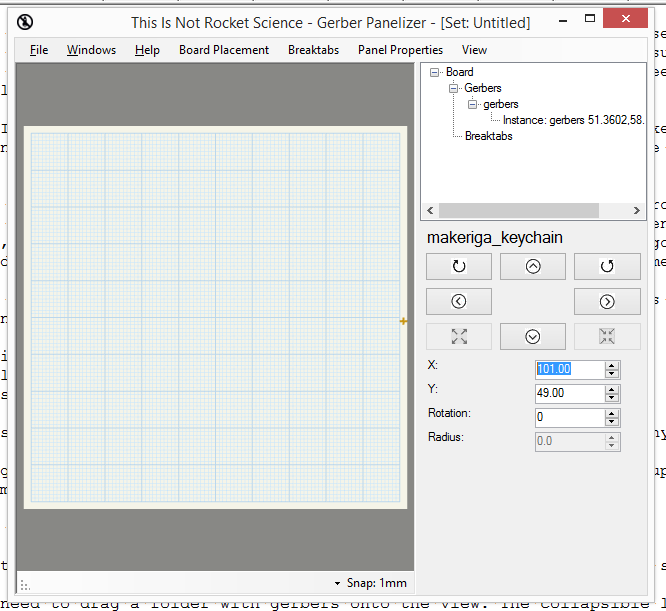
To start, open the GerberPanelizer tool. Go to File->New:
![]() You'll get a 10x10cm panel view. If it's not the case, or you want another size, you might change panel parameters in "Panel Properties".
You'll get a 10x10cm panel view. If it's not the case, or you want another size, you might change panel parameters in "Panel Properties".
Now, you need to drag a folder with gerbers onto the view. The collapsible list in the right top corner will indicate there's a board and, if you're lucky, it's going to appear on the field, too.
Necessary: leave some distance between adjacent boards: the mill bit that will be milling out the board outline has to have some place to move. Good distance is 2mm and up.
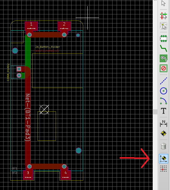
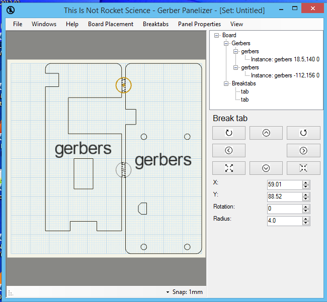
After we placed some boards, we need to place tabs connecting them, and I think it makes sense to do it manually. Hover mouse cursor on the space between the board and press T on keyboard, you're going to get a circle. Move that circle to the place where you want a tab and it'll link two boards. If it won't be able to, the circle outline will be red and it'll give a warning in small text, hopefully.
![]()
Too many tabs will make dividing boards hard. Not enough tabs will give a chance of boards breaking off and getting lost after milling. I more or less have one tab per each board in total, there's also "1 tab per 3cm" rule of thumb. This is OK:
![]()
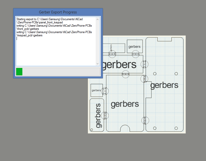
Now, once you've rotated, moved and linked all the boards, press the File -> Export Merged Gerbers button, and make a new folder somewhere to store the gerber files in:
![]() That's it, your gerbers are being linked together. In a short time, the tool will automatically open your image viewer software with pictures of back and front of your boards (those pictures will also be saved in the folder with the gerbers taht just got created). Now zip the gerbers up and send them off to fab!
That's it, your gerbers are being linked together. In a short time, the tool will automatically open your image viewer software with pictures of back and front of your boards (those pictures will also be saved in the folder with the gerbers taht just got created). Now zip the gerbers up and send them off to fab!
![]()
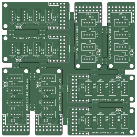
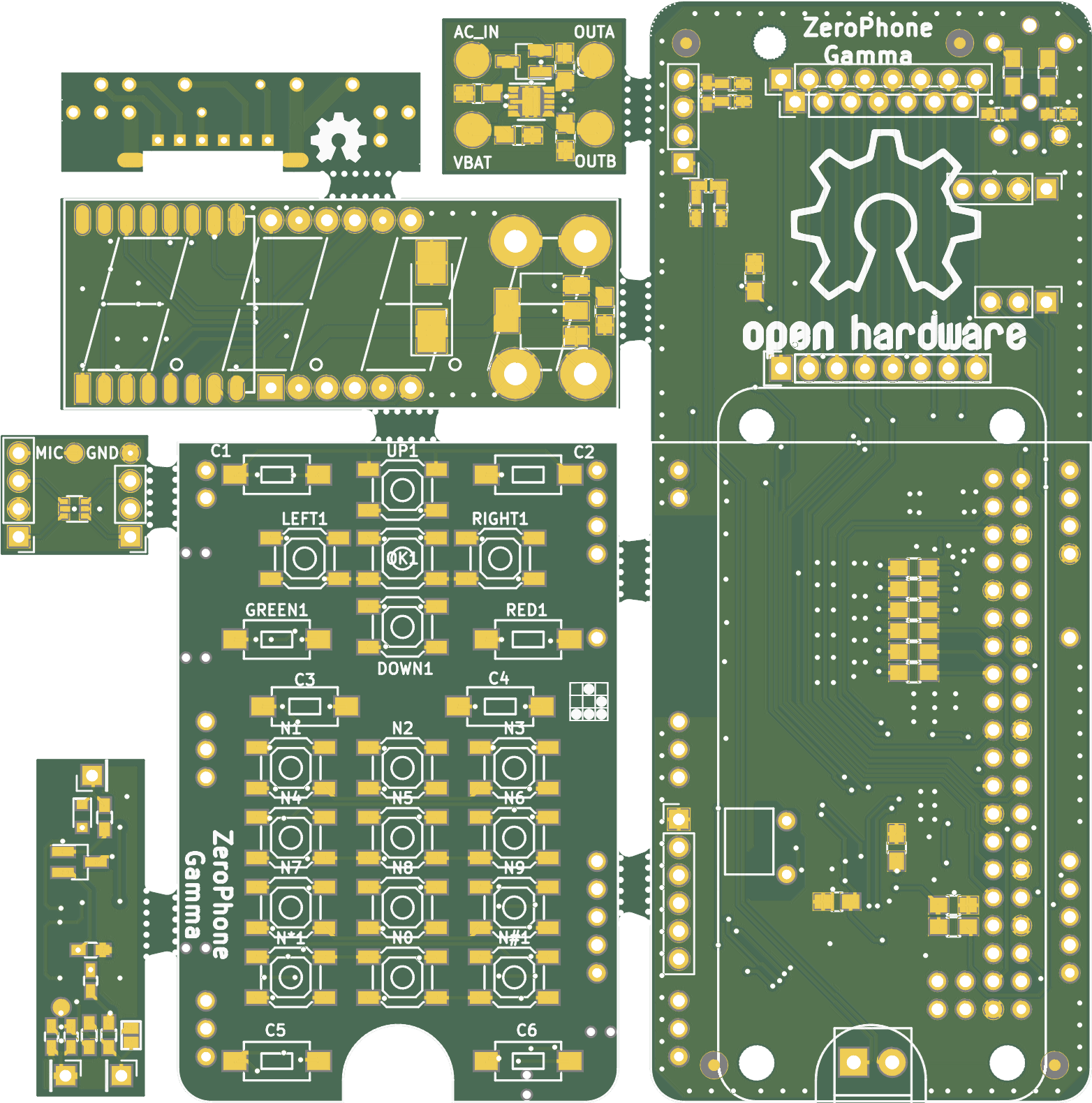
Small PCBs for panelizing + tutorial
Ordering a 10x10 board with only 10x4 taken? Panelize one of these!


 Tabs with mousebites (inner area is not actually filled) - picture
 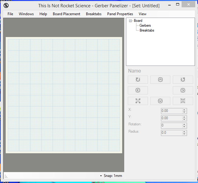 You'll get a 10x10cm panel view. If it's not the case, or you want another size, you might change panel parameters in "Panel Properties".
 That's it, your gerbers are being linked together. In a short time, the tool will automatically open your image viewer software with pictures of back and front of your boards (those pictures will also be saved in the folder with the gerbers taht just got created). Now zip the gerbers up and send them off to fab!
