-
v2.0
09/27/2018 at 21:01 • 0 commentsOkay, I owe some explanations about this project.
•
For v1.0 of the µHVPSU, I blindly followed an existing schematic of a similar design, that worked (or at least seemed to). So I ordered my PCBs and parts, assembled one, and it didn't work. So I assembled a second one, being extra careful, and it didn't work either. I got so annoyed about it that I decided to shelve this project. Until now !
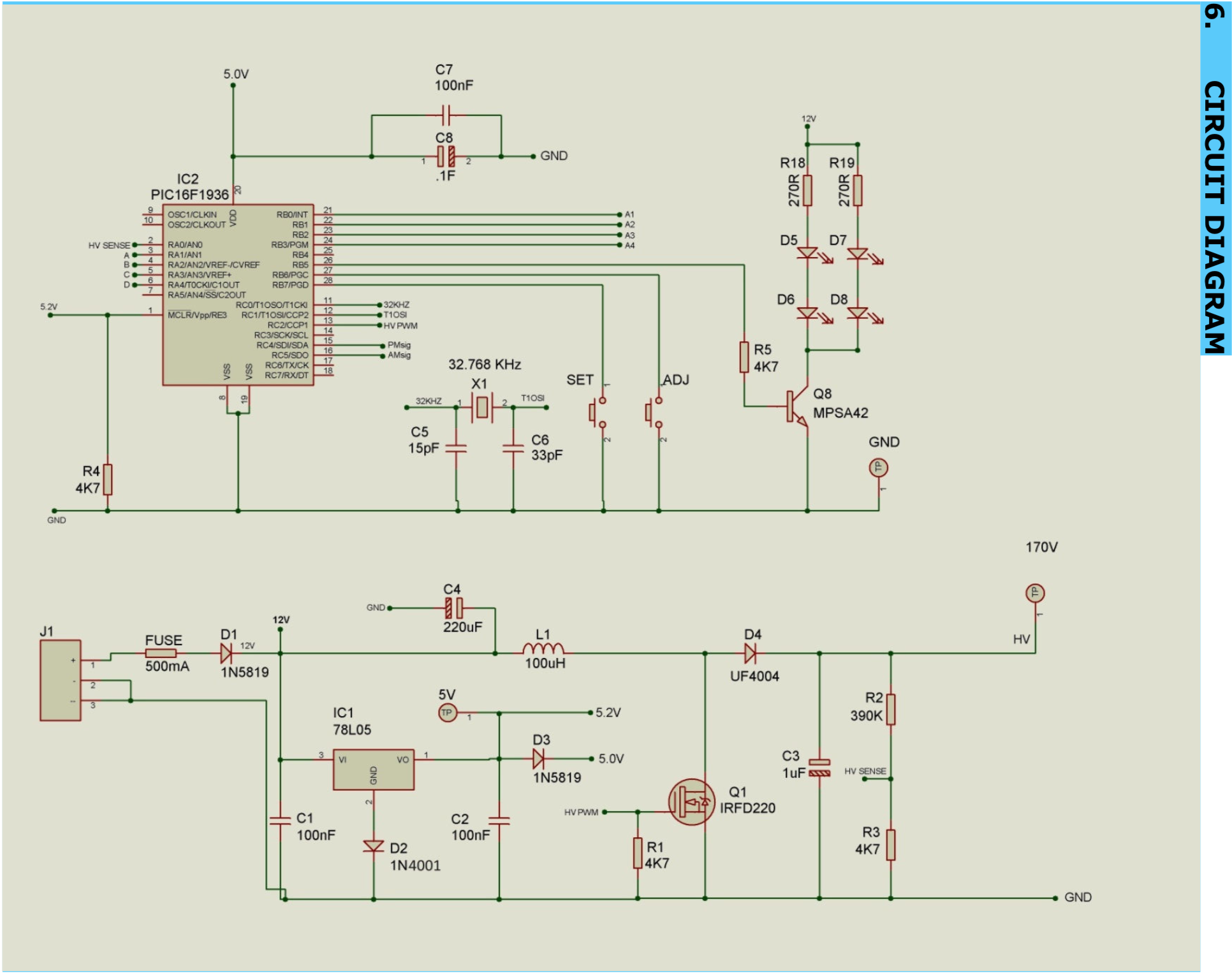
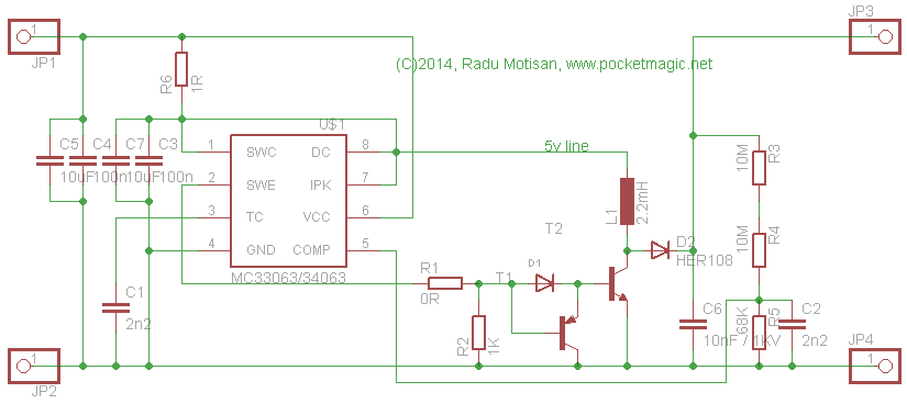
After hunting on eBay for Nixie tubes, I stumbled on many nixie clock kits and PCBs, with documentation, and most importantly, a schematic. What was really redundant was the use an analog input pin and a PWM output pin of the main µC as the mais DC-DC step-up converter. So I decided to base my new design on one of these schematics.
Here's what I'm talking about :
![]()
This particular clock kit uses a PIC microcontroller, which is fine, but it's a bit too much of an overkill for this project.
Instead, I will use an ATTiny44 as they are widely available on eBay at a cheap price (about 6$ for a pack of 10), and they allow me to program them with the Arduino IDE, which I'm already really familiar with ^^ So that gives me a lot more flexibility.
•
So yeah, that's it for this log ^^ I'll post again when I have something interesting to say, or when all the new components have arrived :)
•
P.S.: M.daSilva and I have decided to make a spreadsheet, in which all of our Nixie tube types and quantities are listed; we have gathered a total of more that 600 tubes (400+ if you don't count the IN-3's)
I guess we'll have enough to make some interesting projects ^^
-
UPDATE : This project is not dead yet !!!
09/27/2018 at 09:36 • 0 commentsIt’s been a while ^^
•
As you saw in the title, I decided to work on this project again, as a friend and myself have ordered over 200 Nixie tubes together, so we need some way to power them.
For the second version, I thought of a *wonderful* process in order to make sure the design works; it’s called [insert WordArd] « Prototyping »
Anyway, I thought of using a microcontroller instead of a dedicated dc-dc converter IC, as it would give me more flexibility (and perhaps custom features) I couldn’t have with the IC I was using.
•
So stay tuned for the next log that I will publish as soon as the components arrive from China ^^
-
Quick thing
01/05/2017 at 18:04 • 0 commentsJust a quick thing I would like to say ^^
I made a document for the BOM which I will update a lot while I'm ordering, assembling and testing the µHVPSU. So in order for you to always have the latest file, I made a shared Keynote document, which you can find here.
That's all ^^
N.B.: Why a Keynote document instead of excel or something else ? Well I use the Apple "iWork" and "iCloud" environnement a lot and I'm really comfortable with that (yes you can say I'm a fanboy, yes..). Oh yes also, sorry for the adfly link ¯\_(ツ)_/¯
-
Ordering PCBs
01/03/2017 at 17:35 • 0 comments![]()
The PCBs are ordered !! As you can see, the size of them is about 14mm by 23mm,. that's small enough for me ^^
As you can also see, the price was 13.95$ for ~10 PCBs (so 0.1395$ each). I will calculate the exact cost when I have received the PCBs, as there's a chance I get more than 10 :p
If this project works, I will put a link somewhere where you will be able to buy the PCB directly on DirtyPCBs.
If you want to see the DirtyPCBs Gerber renderings, you can follow this link ^^
-
Second step : the PCB
01/03/2017 at 16:40 • 0 commentsAs the name implies, it has to be small.
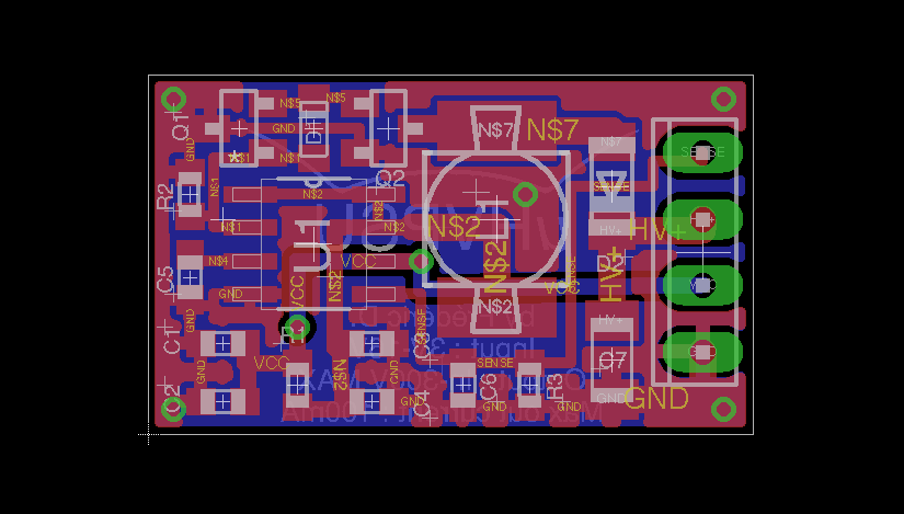
I want all the components to be on the same side, so it's more convenient to solder by hand (as everything is SMD). It's also better if I want to use that module in future designs.
For all the "Low voltage" components, I used 0603 components. They can be tricky to solder by hand, but it's doable. For the high voltage 10nF onboard cap, I used 1206 size (because I had no choice). I may have to use an externah HV electrolythic capacitor, as 10nF may not be enough.
For the transistors I used SOT-23 types. The PNP transistor is a S8550 general purpose transistor, and the High voltage switching transistor is an MMBTA42 300V transistor (the best I found with a great voltage/current ratio), and it's also why the µHVPSU v1 is limited to 300V.
The rectifier diode of the converter is a HER108, because, reasons.. (Okay, it's the one used in the original design).
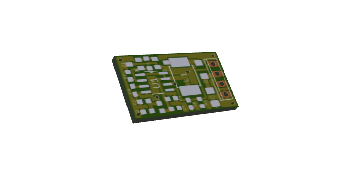
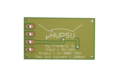
Here are some pictures :
![]()
![]()
![]()
(3D renderings made with this tool (don't pay attention to the green color, the real ones will be white))
-
First step : the schematic
01/03/2017 at 16:20 • 2 commentsAs said in the project details, I based my schematic on the one on this website (link). Here's the said schematic, so you don't have to leave this page ;)
![]() However, I changed a few things in my design.
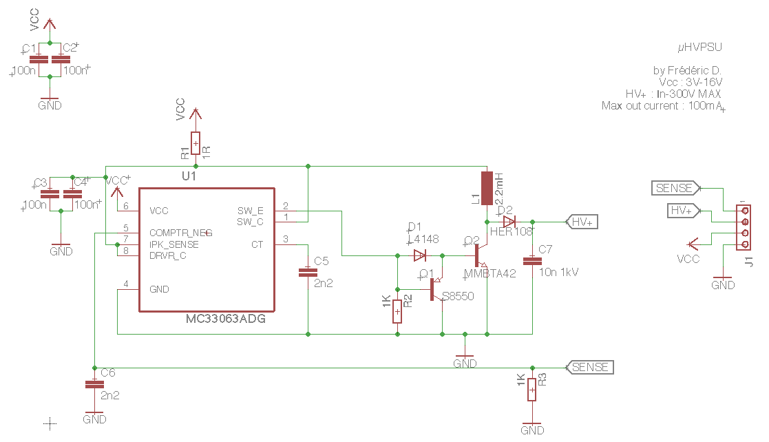
However, I changed a few things in my design.First of all, I used classic 4pin-connector_type-breadboard-friendly-type-thingy to interface the module, so it is easier to implement in other designs.
Secondly, I changed the feedback loop system. In the schematic above, there are fixed resistors, which give the module a fixed (theoretical) output voltage of approx. 370VDC. In my design there is an interface pin where you put a resistor between that pin and the HV output, so you can always control the output voltage.
Oh BTW, here's the formula to calculate the output voltage (found on the MC34063 datasheet)
In my design (I hate saying that, but anyway) R1 is has a fixed value of 1k. You can choose the value of R2 by putting a resistor between the "HV+" pin and the "Sense" pin.
Here's my version :
![]()
All the files can be found in the "Files" tab of the project.
 Frédéric Druppel