“Sinclair video generation is like a dog's walking on his hind legs. It is not done well; but you are surprised to find it done at all.”
To make the experience fit your profile, pick a username and tell us what interests you.
We found and based on your interests.
zx81_plus_38_video_real_resistors_transistor_input.txtUpload this to https://www.falstad.com/circuit/circuitjs.html to try my video output circuit.plain - 1.96 kB - 02/02/2026 at 06:04 |
|
|
ZX81plus38rev1,9.pdfThe board I am building.Adobe Portable Document Format - 321.15 kB - 12/13/2025 at 22:39 |
|
|
ZX81plus38_BOM_revision 1.10-keith (1).odsList of things I have or haven't fitted yet. I'm omitting the tape circuitry, because I have no tapes or tape player.spreadsheet - 20.68 kB - 05/31/2025 at 22:49 |
|
|
2560px-ZX81plus38_revision_1.9_schematic.pngThe board I am building, as an image file.Portable Network Graphics (PNG) - 374.91 kB - 04/30/2025 at 01:15 |
|
|
2026-01-10
Looking at the ZX81+38 video buffer, it seems to have puzzling faults.
When active, the impedance is two 100R resistors in parallel, making 50R. Again, wrong. Two 150R resistors might fix that, but I suspect this is not the correct way to do it. I expected a low-Z buffer with a 75R series resistor to the output socket.
SYNC low shuts off all base current, and the resistors do not present a 75R impedance. Just a 100R to ground. The designer specified a Schottky diode to ensure the base voltage goes lower than the transistor's switch-on voltage.
In practice, you have to have the transistor conducting a bit, to keep it low-impedance. You add a DC offset small enough to be seen as 0V by the monitor.
R48 and 49 are 470 and 1000 ohms, so V_base = 1.6 or 5 volts. Less V_be of 0.7 volts, V_emitter = 0.9 or 4.3 volts. The 0.9 volts is halved to 0.45 at the socket, but 4.3 becomes 2.15. This is 1.7 volts video range.
A proper video signal has 0.3 volt sync depth, and 0.7 volt picture signal depth.
After looking at how others had done this 1-transistor solution, I concluded that none of them were well designed at all. Atari were notoriously bad at this. I expected better of Acorn, but some of their circuits don't stand up to analysis or have potentiometers for the user to twiddle for best results.
So I had a go at designing my own, working back from the proper standard video levels.
Here is my first go:
It assumes an ideal transistor, with infinite gain and zero R_base_emitter, and that the V_base_emitter and diode V_forward are 0.7 volts.
I started with biasing the transistor for white level, then sync level, then black level.
Sync low overrides the video_in level. As you can see, I deliberately used a PIN diode for D1 so the base is biased to conduction (0.7) and resistor R2 adds 0.2V to make the sync level 0.1 volts at the monitor.
D2 also adds 0.7 volts, R2+R3 = 480R to set the black level output.
When Sync is high and video is high, R1...4 set the white level output.
The ideal resistor values soon got off the E24 series, and I don't have the time to work out the best way to improve the values. Especially because the actual resistors will diverge from ideal when dealing with real (non-ideal) transistors and diodes.
I had a second attempt using diodes to control the base voltage. Diodes are more expensive than resistors but my time is more expensive than it is worth to find the best resistor combinations.
It uses 1 more diode, 2 fewer resistors and the resistors are all E24:
This makes use of the fact that PIN diodes have V_f about the same as the video picture depth range, i.e. 0.7 volts. D1 counters V_be, D2 adds an output bias voltage, and D3 adds 0.35 volts sync depth (a tad over the official 0.3 volts).
In the real world, the transistor has a non-zero R_be, which should be subtracted from R4. This is why you often see resistors less than 75R in this position in similar emitter-follower circuits. Typically 68R.
R_base_emitter = V_thermal / I_collector
where
In this circuit, the latter is 17.63 mA so R_base_emitter is about 1.45 R. so R4 of 75R is close enough.
Diode V_f and transistor V_be vary with current and temperature. Check data sheets to make sure they have the right current flowing through them to get 0.7 volts V_f. This looks to be about 3mA at 20C. That would need R1 to be (5-0.9)/0.003 = 1367R and thus R2 = 2050R. The nearest E24 values of
1300 and 2000 set V_white = 1.165 volts.
1500 and 2200 set V_white to 1.136 volts.
1000 and 1500 set V_white to 1.15, with 2mA during white output.
During black output, R2 steals some current from the diodes, so 3.4mA flows in R1 and 1.07 ma through R3, meaning 2.33 mA flows through the diodes.
In practice, most monitors...
Read more »2023-09-02
This is the approach I have decided upon.
This has the following advantages
The memory map should look like this:
/* RAM onboard: a a a a a a a a 1 1 1 1 1 1 5 4 3 2 1 0 9 8 00h,02h 0 0 0 0 0 0 x 0 ZX81 RAM patches at 00XXh and 02XXh 0x20 0 0 1 0 0 x x x G007 RAM (2k space) 0x30 0 0 1 1 0 x x x Spare RAM ROM unified: 0x0c 0 0 0 0 1 1 0 0 ZX81 ROM patch 0x28 0 0 1 0 1 x x x G007 ROM (2k space) 0x38 0 0 1 1 1 x x x Spare ROM RAM expansion: 0x40 0 1 0 x x x x x RAM expansion (8k) 0x40 0 1 x x x x x x RAM expansion (16k) 0x80 1 x x x x x x x RAM expansion (above 32k) Intermediate terms: */ RAM_patches = !a15 & !a14 & !a13 & !a12 & !a11 & !a10 & !a8 ; ROM_8k_at_0000h = !a15 & !a14 & !a13 ; RAM_2k_at_2000h = !a15 & !a14 & a13 & !a12 & !a11 ; ROM_2k_at_2800h = !a15 & !a14 & a13 & !a12 & a11 ; RAM_2k_at_3000h = !a15 & !a14 & a13 & a12 & !a11 ; ROM_2k_at_3800h = !a15 & !a14 & a13 & a12 & a11 ; /* The terms above simplify if you wish to minimise logic: */ RAM_at_2000h_and_3000h = !a15 & !a14 & a13 & !a11 ; ROM_at_2800h_and_3800h = !a15 & !a14 & a13 & a11 ; /* However I shall leave them unsimplified so they can be modified more easily: */ /* Drive pins: */ RAM_expansion = mreq & a15 // at 8000h, above 32 + mreq & a14 // at 4000h or C000h RAM_onboard = mreq & RAM_2k_at_2000h + mreq & RAM_2k_at_3000h; /* NB if onboard RAM is 8K or less, then RAM at 00XX and 02XX are aliased at 20XX and 22XX respectively. If you have more, then they are not, and the higher addresses are free for your use. */ ROM_unified = mreq & ROM_8k_at_0000h & !(RAM_patches) + mreq & ROM_2k_at_2800h + mreq & ROM_2k_at_3800h ; /* NB the logic above will probably expand to something like: */ ROM_unified_alt = + mreq & ROM_8k_at_0000h & a11 // 1000h + mreq & ROM_8k_at_0000h & a10 // 0800h, 1800h + mreq & ROM_8k_at_0000h & a8; // 0400h, 0600h, 1400h, 1600h /* So the memory address decoder uses 9 inputs and 3 outputs in: A15...8 !mreq out: ROM_unified RAM_onboard RAM_expansion That leaves 10 pins, up to 7 outputs and 3 inputs or 1 output and 9 inputs. */ memory_refresh = mreq & rfsh; /* clocks a D-type latch to set text or high-res mode */ pixel_latch = graphics_mode & mreq & cpu_clk ; pixel_output = graphics_mode & rfsh ; force_nop_2 = graphics_mode & m1 & A15 ; _rd = rd & a15 + rd & a14 + rd & something ; u9a_latch_d = mreq & _rd & force_nop_2 ; u9a_latch.d = u9a_latch_d; u9a_latch.ar = u9a_latch_d; d7 = _d7 ; d6 = _d6 ; d7.oe = _rd ; d6.oe = _rd ; _d7 = d7 ; _d6 = d6 ; _d7.oe = u9a_latch ; _d6.oe = u9a_latch ;
I suspect the RAM patches may not need to be RAM, but I want to keep it working as near to the original for compatibility reasons.
2023-09-07
Spent a long time thinking.
I think I can get the memory decoder working in a way compatible with the G007 board.
Ian Bradbury's design uses an ATV750 which is like two 22V10 chips in one package, and each output macrocell can have its own clock and set/reset signals.
His logic makes much use of the latter, which is useful because the ZX80 circuit also has multiple clocks and set/reset signals. For that reason I am currently keeping the 74HC74 D-type latches.
The HSYNC logic of the ATV750 will not fit in a 22V10, so I decided to use a 74HC393 counter and a 22V10.
... Read more »2023-08-28
I looked at Ian Bradbury's ZX81 in SPLDs, intending to mop up some of the small-scale-integration chips (2 to 4 input gates) that I don't have, into 22V10 logic chips that I do have. They're handy because they operate at 5V.
The logic is written in CUPL which is quite low level, like assembly language. Most designers have moved on to VHDL or Verilog, which are needed for today's big FPGA chips.
I thought I'd have a go compiling one of the ready-made designs.
There's a Cyclone II EP2C5 Mini Dev Board available dirt cheap and ZX81 code for it at https://www.qsl.net/yt2fsg/zx81/zx81_clone.html which I downloaded, unzipped and opened the project file from Quartus.
First of, it complains that my version of Quartus Lite, 20.1.1, will not compile for Cyclone II.
Okay, I told it to compile for Cyclone IV, which is the device on the DE-NANO that I have.
Next it complained T80s not found. This Z80 model is someone else's project, so I guessed I need to get the latest version.
I went to https://github.com/mist-devel/T80 and downloaded the files as a zip file called T80-master.zip which needed unzipping into a sibling directory called T80. It unzipped into a directory called T80-master so that needed renaming. That fixed that issue.
Now it moans:
Warning (12019): Can't analyze file -- file ../FPGA_ZX8x_shared/*.vhd is missing
where *.vhd is many files. The whole directory is missing!
I eventually found this to be a better source of everything:
https://svn.mavipet.sk/svn/fpga_comps/HW_V1.0/
most of which are Cyclone II but FPGA_ZX81_Full does not get the Cyclone II error message.
But I still get other errors!
2023-08-31
One can add slow mode hardware to a ZX80, but I decided to buy a board with this designed in already.
https://revspace.nl/Buiding_up_and_testing_the_ZX81%2B38_revision_1,9
https://github.com/mahjongg2/ZX81plus38
2023-08-19
I bought these boards on eBay.
The logic board has some nice features. The bus signals are available on a holes for a header, allowing the dreaded RAM-pack wobble to be avoided. The board can take up to 32K RAM, so you don't even need an external RAM pack.
Power is from a USB-B socket. I'll have to check the electric current budget.
On the down side, the clock is a crystal-and-inverter which mean I can't change frequencies by swapping an oscillator can. I think that can be hacked!
The on-board SLOW-mode generator will need hacking to run with a 14.7456 MHz clock. I'll design something that can be easily switched between two frequencies.
The keyboard is on a separate PCB, so no mechanical stress is transmitted to the motherboard. It has the key letters but not the associated keywords.
The boards are due in about a week, so I shall get hunting for components.
2023-08-21
Printed out the circuit diagram and parts list. I have:
What I don't have:
I could use some PAL chips to mop up the random logic. I have plenty and they are easy to modify.
2023-08-23
Boards arrived. I have soldered the key switches to the keyboard.
The motherboard is very packed.
2023-08-25
I fitted 0603 surface mount resistors where there are vertical through-hole resistors.
The ACT574 and HC165 chip are now soldered to the board.
2023-08-31
I have no HC541 chips but plenty of HC245 chips. So I took two HC245 chips and bent pin 1 under the chip and wired it to VCC. I then fitted it to the HC541 sites.
2023-09-27
Fitted SIL sockets for keyboard.
2025-04-25
2025-05-18
I decided to fit all the chips that were not completely used in the HSYNC and PORCH timing. This is basically all of them except U15 (a 74HC11) and U8 (a 74HC4002).
I plan to replace these with a GAL16V8, with more sophisticated timing, for both normal and square pixels.
The signals q7 down to q0 are on U14.
The asynchronous reset is on U15 pin 8.
The output signals PORCH and HSYNC are on pins 1 and 13 of U8 respectively.
So not a huge wiring job. Some pins can be piggybacked on the 74HCT393.
2025-05-29
Shopping around for the last few bits for this project. I wondered why the Mouser 13 MHz crystal in the BOM did not appear in my search for crystals, and I spotted that the footprint is completely incompatible with the PCB. It has leads 2.5 mm apart, while the PCB has holes 4.88 mm apart. The PCB uses an HC49 footprint, not an HC46 footprint. So, the most suitable part seems to be IQD part LFXTAL031646B which is Mouser part 449-LFXTAL031646BULK. Also note that wire-ended crystals will need some insulation from the SMD footprint pads, otherwise the metal body will short-circuit them. See Mouser part 520-700-TFL-9001.
2025-11-11
Fitted R12,14,15, RP1, RP2, X1, original 2364 ROM.
2025-11-12
Applied 5V through USB cable, but failed to boot up. The current drain was exactly 100mA, which makes me wonder if it wanted more but was being limited to the USB peripheral limit. In another USB socket labelled 5V 2.1 A, it was 4.886 volts measured at the power input socket, 4.872 at ROM pin 24.
5V pins connected to each chip.
Sigh, I'm going to have to get out the scope and do a lot of hard work. :-(
2025-11-17
Identified the problem. I was using an original 2364 ROM, which has socket pin 20 (2364 pin 18) = A11, and socket pin 22 (2364 pin 20) = /CE. The latter is permanently wired to nROMCS. The bug...
Read more »This was the quickest way of getting a known-good reference machine.
Alas it is not very hackable, because most of the logic is inside the ULA.
It did come cased with a working membrane keyboard.
I extended the connections to the keyboard using extra-flex wire, allowing operation with the PCB accessible without removing the membrane from the case.
I hacked the ROM socket to accept a modern flash ROM, so that I could experiment with modified firmware.
I removed the 5V regulator and heatsink then wired a 2.1 mm power socket so that could be powered by a common 5V wall-wart power supply.
Attached is the G007 graphics board. I have tried to reduce the RAM-pack wobble by fitting a 32K RAM chip over the G007 ROM chip. D7 and D6 have to go to the edge connector. This should be an easy hack but for some reason it didn't work and I left that hack in that state. It still works with an external RAM pack if the 32K RAM is removed.
2023-09-15
Not working right now, I checked the ROM and RAM address lines. I tied the ROM /WE pin high. Seemed not to work but I had set my TV for white-on-black for my ZX80. Adjusting the controls allowed the ZX81 signal to be seen.
Still not working with the G007, or the DRAM pack, or both.
Create an account to leave a comment. Already have an account? Log In.
Become a member to follow this project and never miss any updates
By using our website and services, you expressly agree to the placement of our performance, functionality, and advertising cookies. Learn More
Anders Nielsen
Keith
Hacker404
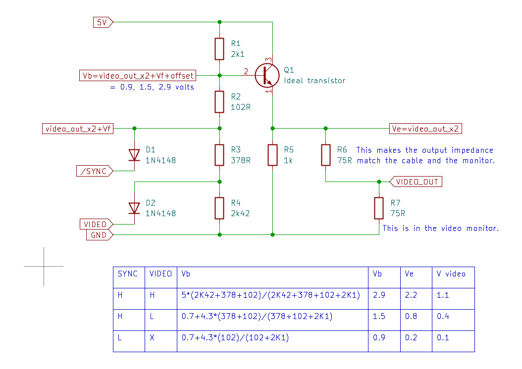
This article might be useful for you: Generating video with correct amplitude and output impedance
https://hackaday.io/project/8537-vga-blinking-lights/log/28258-generating-video-with-correct-amplitude-and-output-impedance